A versatile laser-based apparatus for time-resolved ARPES with micro-scale spatial resolution
Abstract
We present the development of a versatile apparatus for a 6.2 eV laser-based time and angle-resolved photoemission spectroscopy with micrometer spatial resolution (time-resolved -ARPES). With a combination of tunable spatial resolution down to 11 m, high energy resolution (11 meV), near-transform-limited temporal resolution (280 fs), and tunable 1.55 eV pump fluence up to 3 mJ/cm2, this time-resolved -ARPES system enables the measurement of ultrafast electron dynamics in exfoliated and inhomogeneous materials. We demonstrate the performance of our system by correlating the spectral broadening of the topological surface state of Bi2Se3 with the spatial dimension of the probe pulse, as well as resolving the spatial inhomogeneity contribution to the observed spectral broadening. Finally, after in-situ exfoliation, we performed time-resolved -ARPES on a 30 m few-layer-thick flake of transition metal dichalcogenide WTe2, thus demonstrating the ability to access ultrafast electron dynamics with momentum resolution on micro-exfoliated and twisted materials.
I Introduction
Angle-resolved photoemission spectroscopy (ARPES) is a well-established experimental technique used to directly probe the momentum-resolved electronic structure of crystalline materials. The underlying principle of ARPES is the photoelectric effect, which describes the process of photoemitting electrons via the absorption of high-energy photons. The emitted photoelectrons are then characterized in terms of their kinetic energy and emission angle, providing valuable information about the electronic band structure in the form of spectral intensity . Beyond imaging electronic band structure, the spectral intensity encodes information about underlying interactions in strongly correlated systems Damascelli (2004); Sobota, He, and Shen (2021). For example, in materials with strong electron-phonon coupling, ARPES spectra can exhibit a kink in the dispersion at an energy associated with the phonon mode, revealing information about which modes affect the observed electronic properties Wen et al. (2018); Devereaux et al. (2004); Cuk et al. (2005); Ludbrook et al. (2015). Likewise, in materials with strong spin-orbit coupling, ARPES spectra can exhibit a characteristic spin-splitting of the bands, which reflects the coupling between the electron spin and orbital momentum in the crystal lattice Xia et al. (2009).
While equilibrium ARPES has been instrumental in unveiling one-particle dynamics and interactions in correlated systems, the extension of ARPES into the time domain enables the study of light-induced multi-particle dynamics and out-of-equilibrium phenomena in bulk materials. Time- and angle-resolved photoemission spectroscopy (TR-ARPES) combines ARPES with a pump-probe approach allowing for the simultaneous exploration of temporal, energy, and momentum degrees of freedom (DOF) Boschini, Zonno, and Damascelli (2023); Smallwood, Kaindl, and Lanzara (2016). This technique has facilitated the observation of unoccupied states Sobota et al. (2012), the generation and subsequent decay of phonons Perfetti et al. (2007); Sobota et al. (2014a); Na et al. (2019), Bloch Floquet states Wang et al. (2013); Mahmood et al. (2016), and photoinduced phase transitions Perfetti et al. (2006); Okazaki et al. (2018)–observations that were otherwise inaccessible using equilibrium ARPES.
More recently, stimulated by advancements in exfoliation techniques and the nascent field of twistronics, which have led to the emergence of interesting physical phenomena and novel phases of matter in the two-dimensional counterparts of bulk materials Novoselov et al. (2004, 2005), a major effort has been invested in the development of equilibrium ARPES approaches with high spatial resolution, i.e. -ARPES and nano-ARPES. These experiments are enabled by light sources capable of tightly focusing the probe photon beam to sub-10 m (-ARPES) or sub-1 m (nano-ARPES), which are capable of probing exfoliated flakes with spatial dimensions on the order of 10 m Cattelan and Fox (2018); Mo (2017). These techniques have provided a route to answer questions pertaining to the role that dimensionality plays in the momentum-resolved electronic properties of exfoliated materials, heterostructures, and highly inhomogeneous samples. To this end, it is equally desirable to extend also TR-ARPES approaches towards micrometer scale spatial resolution.
Time-resolved -ARPES enables the tracking of light-induced electron dynamics in exfoliated and inhomogeneous materials: while an intense pump pulse optically excites the system from its ground state, a subsequent micro-meter sized probe pulse photoemits the excited electrons. A lower photon energy source in the ultraviolet (UV) regime between 5.9 - 7 eV is typically generated from nonlinear optical crystals such as BaB2O4 (BBO) or KBe2BO3F2 (KBBF) Koralek et al. (2007); Faure et al. (2012); Ishida et al. (2014); Yang et al. (2019); Bao et al. (2022), while higher photon energy sources in the extreme UV regime, capable of reaching photon energies exceeding 20 eV, are typically generated via high-harmonic generation (HHG) in a gas Mills et al. (2019); Sie et al. (2019); Puppin et al. (2019); Keunecke et al. (2020); Lee et al. (2020). Laser-based systems capable of achieving micron-scale spatial resolution typically use a combination of external expanding telescope schemes and focusing optics mounted in vacuum to achieve spatial resolutions better than 5 m Iwasawa et al. (2017); Xu et al. (2023). Moreover, a time-resolved -ARPES system should encompass a mechanically-stable sample manipulator with cryogenic cooling capabilities, diagnostic tools to characterize the spot size and pointing stability of the laser pulses, as well as a high-resolution camera to locate and image exfoliated flakes in front of the electron detector.
In this work, we describe the development of a 1.55 eV pump and 6.2 eV probe source for time-resolved -ARPES with tunable spatial resolution down to 11 m (Section II) and demonstrate the performance of our system by: (1) resolving the surface inhomogeneities that are responsible for increased spectral broadening in the topological insulator Bi2Se3 (Section III); and (2) measuring the time-resolved electronic properties of an in-situ exfoliated sub-30 m WTe2 flake on Ag(111) (Section IV).
II Experimental Setup
II.1 System Information
ARPES measurements are performed in the UBC-Moore Center for Ultrafast Quantum Matter equipped with a SCIENTA-Omicron DA30-L high-resolution hemispherical electron analyzer, in a UHV chamber with base pressures lower than 5 10-11 Torr. The spectrometer is equipped with a helium-flow cryogenic manipulator, providing stable temperature control of the samples to sub-10 K temperatures. The manipulator possesses five motorized DOF, which consist of two rotational () DOF to orientate the sample, and three translational DOF (x,y,z) [see Fig. 1(c)].
The vibration of the cryostat and, as a result, of the sample position follows a Gaussian distribution , where and are the standard deviations in the sample position measured to be 4.6 m and 3.3 m in and , respectively. On the spatial scale of the tightly-focused probe, these variations cannot be neglected and will contribute to the total spatial resolution of our apparatus, as will be discussed in Section II.3.
The system also features a load-lock and preparation chamber with the second stage equipped with a sputter gun and e-beam heater for sputtering-annealing of samples.
II.2 Light Source
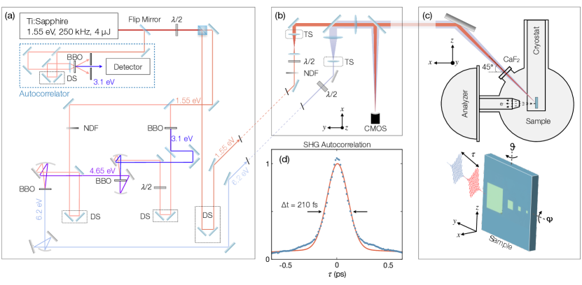
A schematic of the 6.2 eV generation process and 1.55 eV pump propagation is shown in Fig. 1(a). The ultrafast light source is based on a Ti:sapphire laser (Vitesse Duo and regenerative amplifier RegA 9000 by Coherent), generating 150 fs pulses [characterized from the cross-correlation of two 1.55 eV pulses using a second harmonic generation (SHG) autocorrelator, as shown in Fig. 1(d)] at a central wavelength of 800 nm at a repetition rate of 250 kHz, and an output pulse energy of 4 J. The source output is separated into two branches which form the basis of both the 6.2 eV probe and the 1.55 eV pump. A portion of 1.55 eV output is focused onto a BBO crystal for SHG producing 3.1 eV, which is recombined with the residual 1.55 eV on a second BBO for third harmonic generation (THG), producing 4.65 eV light. In the final stage of generation, the 4.65 eV is combined with 1.55 eV on the third BBO to generate 6.2 eV.
The pump and probe are directed to an optical bench [Fig. 1(b)] where the beams propagate through expanding telescopes and subsequently are recombined to propagate collinearly to a focusing lens. The pump and probe enter the UHV chamber through a CaF2 window at 45∘ with respect plane of the sample [Fig. 1(c)]. The expanding telescopes are used to maximize the diameter () of the beams before they are focused by a lens with focal length to minimize the 1/e2 waist radius (, assuming >> and M1). In addition to minimizing , the spacing between the lenses constituting the expanding telescope plays a vital role in defining the divergence of the beam incident on the focusing lens , which, in turn, influences the focal position. We exploit this concept by incorporating a motorized translational stage capable of displacing one of the expanding telescope lenses, facilitating user control over the pump and probe 1/e2 radii incident on the sample between 17 - 450 m, and 7.9 - 200 m, respectively.
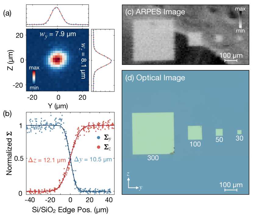
The pump and probe beam profiles are monitored by a high-resolution camera equipped with a complementary metal-oxide semiconductor (CMOS) sensor for simultaneous monitoring of the pump (800 nm) and probe (200 nm), which is positioned such that the camera sensor and sample position are equidistant from the focusing lens. An image of the 6.2 eV beam profile near the focal position is shown in Fig. 2(a) with a horizontal () and vertical () 1/e2 radius of 7.9 m and 8.1 m, respectively, as determined by a two-dimensional Gaussian fit to the beam profile in the form . In the next section, we discuss how we combine the optical beam characterization with the sample position vibrations mentioned in Section II.1 to define the overall effective spatial resolution of our system, and demonstrate a method for directly measuring it using ARPES.
II.3 Spatial Resolution
As mentioned in Section II.1, the vibration of the cryostat is non-negligible on the spatial scale of the probe, and will increase the area of the sample exposed to the probe. To account for the contribution of sample position vibrations on the spatial resolution of our system, we consider the Gaussian profile obtained by convolving with the beam-profile contribution , to obtain: , where the total 1/e2 radius is given by . Because of a combination of the beam projection on the sample, elongating the probe in the vertical direction, and a minor astigmatism of the probe, we measure the horizontal () and vertical () spatial resolutions separately, defined by the full-width at half-maximum (FWHM) of a beam with waist radii ( ) and ().
Our approach to quantifying the spatial resolution builds on the classical "knife-edge" measurement, in which a blade eclipses a focused laser beam profile [y] while a photodetector situated behind the blade measures the transmitted power, typically in a form proportional to , enabling a direct measurement of the FWHM = Firester, Heller, and Sheng (1977). To implement this measurement design in a way that is compatible with ARPES, we replace the total transmitted power measured by a photodetector with the energy- and angle-integrated photoemission signal acquired in the spatial acquisition mode of the DA30-L hemispherical electron analyzer as the manipulator sweeps the horizontal () and vertical () edge of the Si/SiO2 sample across the profile of the probe. Similar to the optical knife-edge method, the resulting signal follows an error-function distribution in both the and , from which the horizontal () and vertical () spatial resolutions can be measured.
The background-subtracted and normalized total photoemission signal, detected across the horizontal (blue) and vertical (red) profile of the 6.2 eV beam as a function of cryostat position is shown in Fig. 2(b). The profiles displayed correspond to the sample-vibration-limited spatial resolution of = 10.5 0.4 m, and = 12.1 0.4 m (projection corrected). In an effort to provide a straightforward indicator of the overall spatial resolution of our system, we define the effective spatial resolution as the FWHM of a 2D Gaussian with an area equal to that enclosed by an ellipse with radii and , resulting in = 11.3 0.3 m.
For a second test, we fabricate a structure that can be measured both optically and by photoemission for a direct comparison. Here, the sample consists of a Si/SiO2 wafer, covered with a 5 nm layer of evaporated Ti to enhance the adherence of the 45 nm thick Au layer in a cascading-squares pattern (from 300 - 30 m) fabricated by photo-lithography, as illustrated in the Fig. 1(c). A high-resolution optical image of the sample in UHV is shown in Fig. 2(d), for comparison with the ARPES image [Fig. 2(c)] obtained by raster scanning the sample across the profile of the 6.2 eV beam, and plotting the value obtained in spatial mode binned in 10 10 m2 regions. This map serves to highlight the imaging capability of our system, as we are able to locate and acquire meaningful spectral information from samples smaller than 30 m.
II.4 Temporal Resolution
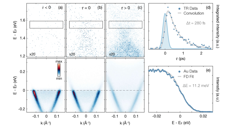
To assess the temporal resolution of our instrument (t) and fine-tune the spatial overlap of the pump and probe, we use the topological insulator Bi2Se3, of which the photoinduced dynamics has been thoroughly characterized Sobota et al. (2012, 2014b). The temporal resolution is defined as the duration of the cross-correlation between the probe and pump pulses given by , where () is the pulse duration of the probe (pump), and is measured experimentally by tracking the relaxation dynamics of the direct-transition population at 1.55 eV above E. For this measurement, Bi2Se3 was cleaved in-situ at 10 K and pumped with p-polarized 1.55 eV photons at an incident fluence of 0.76 mJ/cm2; the equilibrium spectra of the topological surface state (TSS) are shown in the bottom panel of Fig. 3(a), where the Dirac-point is located 300 meV below E.
In the top panels of Fig. 3(a-c), we show the evolution of the direct transition population into the electronic states more than 1.55 eV above E. The time-resolution-limited onset and subsequent relaxation of the direct transient population 1.55 eV above E [boxed region in the top panels of Fig. 3(a-c)] are shown by blue circles in Fig. 3(d), and fit to an exponential decay convolved with a Gaussian function (solid grey line); the FWHM of the Gaussian function [shaded blue region in Fig. 3(d)] returns a total temporal resolution of 280 fs. This cross-correlation of pump and probe pulses, together with the earlier autocorrelation determination of 150 fs [Fig. 1(d)], assuming a Gaussian pulse shape, allows us to extract 236 fs.
II.5 Energy Resolution
The total energy resolution of the system is a combination of the analyzer contribution and the bandwidth of the laser . To measure the total energy resolution, we use a Si/SiO2 wafer fabricated using the method described in Section II.3, and uniformly cover the surface in-situ by evaporating Au at 10 K. ARPES spectra were collected using the 6.2 eV photons with a straight analyzer entrance slit width of 0.05 mm and pass energy of 5 eV. The resulting angle-integrated spectrum is shown in Fig. 3(e). We fit this measured intensity to a Fermi-Dirac distribution, with a width proportional to kT, convolved with a Gaussian function, representing the total energy resolution, , which was measured to be 11.2 meV. Assuming >> , from the previously determined 236 fs the upper limit of the time-energy bandwidth product of our system is 2643 meVfs, which is 1.4 times the transform-limited time-bandwidth product for a Gaussian-shaped pulse,which has a minimum value of Et mevfs Gauthier et al. (2020).
III Bi2Se3 Spatial Resolution
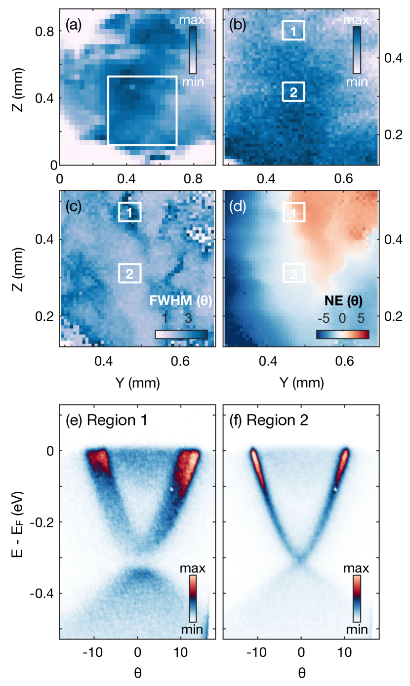
The spectral features measured by ARPES inherently possess a finite linewidth arising from fundamental many-body interactions, where increased electronic scattering reduces lifetime and, consequently, leads to broadening Damascelli, Hussain, and Shen (2003); Iwasawa (2020). However, before drawing conclusions about electronic interactions from these spectral features, it is essential to consider how extrinsic factors contribute to spectral broadening, and may potentially overshadow the intrinsic linewidth. These extrinsic factors include angular uncertainty introduced by sample surface inhomogeneity (originating from inhomogeneous chemical doping, or the presence of several domains, for example), and stray field effects arising from a large difference in the work function between the sample and the substrate or surroundings, which are likely to distort the path of low-kinetic energy electrons Fero et al. (2014). While the primary motivation for developing a -ARPES setup is to investigate the electronic properties of exfoliated crystalline materials, another objective is to enhance data quality obtained from large samples by minimizing the contribution of extrinsic factors that overwhelm inherent spectral linewidth measured. Here, by taking advantage of the full control of the effective spatial resolution, we show that microscopic inhomogeneities of the macroscopically flat surface of the well-studied Bi2Se3 topological insulator lead to a considerable broadening of the ARPES lineshape.
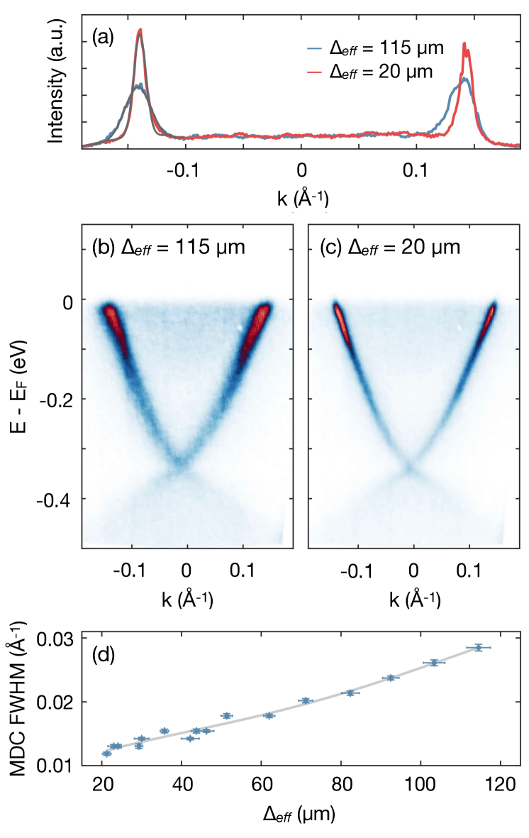
Measurements on Bi2Se3 cleaved in-situ were performed at 10 K while systematically varying the size of the 6.2 eV probe to obtain ARPES spectra corresponding to total spatial resolution values between 20 - 115 m. Spectra acquired with values of 115 and 20 m are depicted in Fig. 4(b) and (c), respectively. For a direct comparison between these spectra, the momentum distribution curves (MDCs) at E are shown in Fig. 4(a), superimposed with a Gaussian fit plus polynomial background (solid grey line), from which the FWHM of the TSS near E is extracted. The spectral width of the TSS, as determined by the FWHM from the composite fit to the MDCs, increases from 0.012 to 0.029 , more than double, when the is increased from 20 m to 115 m, demonstrating how strongly the measured spectral linewidth can be tied to extrinsic sources, rather than intrinsic factors. To further demonstrate this dependence, we extract the width of the TSS for values ranging from 20 to 115m by systematically changing the spot size of the probe incident on the sample; the FWHM of the MDCs as a function of spatial resolution is shown in Fig. 4(d), where we report a clear correlation between the spectral broadening and probe spot-size.
Before investigating the precise origin of this extrinsic spectral broadening becoming more prominent the larger the beam spot, we will briefly mention one caveat to the -ARPES approach, namely the ever-increasing contribution of space-charge effects which can in principle be an additional source of extrinsic sample broadening. A tightly-focused pulsed light source can emit a dense cloud of spatially and temporally confined photoelectrons that experience significant Coulomb repulsion, leading to spatial spreading and kinetic energy broadening Hellmann et al. (2009); Graf et al. (2010). This is however not a concern here: in the context of the results shown in Fig. 4, if space-charge effects were contributing we should have reported a progressive increase in the linewidth as we increase the probe fluence upon reducing the beam spot, at variance with what we observed experimentally. Additionally, space charge effects were mitigated prior to measurements by reducing the probe spot size to the minimum, and subsequently attenuating the probe until no shift of the Fermi-level is observed with the tightest possible focus.
To further investigate extrinsic contributions to the spectral broadening, we use the tightly-focused 6.2 eV photons in combination with high-resolution sample scanning to resolve surface inhomogeneities that could be potentially contributing to the observations presented in Fig. 4. In Fig. 5(a),(b) we show an ARPES spatial map of the entire cleaved Bi2Se3 sample [Fig. 5(a)], and a high-resolution scan of the subsection [Fig. 5(b)] enclosed in the white boxed region in Fig. 5(a). Within each 30 30 m2 (5 5 m2) pixel in Fig. 5(a) [Fig. 5(b)], ARPES spectra are acquired in angular mode, and the photoemission signal within 70 meV of the Fermi level is integrated over all angles ( 20∘), which defines the color scale of this image. The high-resolution intensity map in Fig. 5(b) appears macroscopically uniform, with little variation in the integrated intensity observed over this region of the sample. However, variations become apparent when the FWHM of the TSS close to E [Fig. 5(c)] and relative angle of normal emission [Fig. 5(d)] is extracted for each 5 x 5 m2 region shown in Fig. 5(b).
Even with an inhomogeneous sample surface such as the one displayed here, we are able to obtain high quality and sharp spectral features [Fig. 5(e), for example] by reducing the probe size to dimensions smaller than the surface variations. Additionally, by minimizing the contribution of extrinsic sources, we begin to approach a regime where the spectral broadening is representative of the intrinsic many-body interactions, as shown by the gradual trend towards sharper linewidths observed in Fig. 4(d).
IV WTe2
Beyond resolving surface inhomogeneity, the small-spot capability of our system is useful for studying ultrafast dynamics in exfoliated materials and stacked/twisted layers on the order of tens of m. In this section, we use in-situ exfoliated transition metal dichalcogenide (TMD) WTe2 to showcase our time-resolved -ARPES apparatus as a method for measuring the electronic properties of exfoliated materials. WTe2 is a type-II Weyl semimetal exhibiting large magnetoresistance Tang et al. (2017); Shi et al. ; Das et al. (2019), and has previously been the subject of extensive TR-ARPES and -ARPES studies owing to its potential as a platform for the study of topological quantum effects Cucchi et al. (2019); Hein et al. (2020); Caputo et al. (2018); Wu et al. (2016). In addition, successful exfoliation in UHV of WTe2 via kinetic in-situ single-layer synthesis (KISS) technique has been reported Grubišić-Čabo et al. (2023), making WTe2 a good candidate for a demonstration of the performance of our time-resolved -ARPES setup for the study of ultrafast dynamics in exfoliated materials.
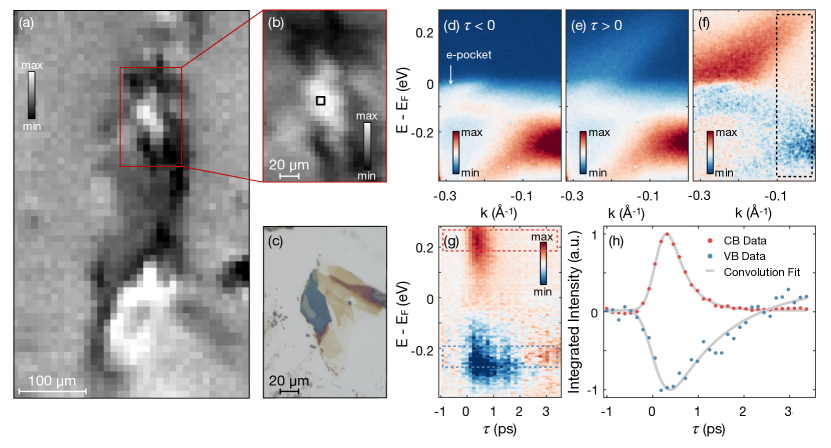
A 400 x 400 m2 Ag(111) substrate was prepared by 1 keV Ar-ion sputtering and 550 K annealing. Bulk WTe2 was cleaved in-situ, revealing an atomically clean surface, and exfoliated onto the Ag(111) substrate using the KISS method, which consists of stamping the clean Ag(111) substrate with the surface of the cleaved bulk crystal. Flakes of WTe2 were located by scanning the sample in 30 m steps as shown in Fig. 6(a), where the color scale represents the energy and momentum integrated photoemission intensity within a region 200 meV below E. A high-resolution (5 m) spatial scan of this flake is shown in Fig. 6(b) with a direct comparison to the corresponding optical contrast image in Fig. 6(c), revealing a 30 m flake of WTe2. The sample was orientated along the direction and probed with p-polarized 6.2 eV photons, as shown in Fig. 6(d), where we observe the electron pocket centered around k|| = -0.3 . Figure 6(f) displays the differential ARPES map [I( > 0) - I( < 0)], where we observe a transient enhancement in the population of the electron pocket above E (red area) along with a suppression of spectral weight in the valence band below E (blue area), consistent with previous observations Hein et al. (2020); Bruno et al. (2016); Caputo et al. (2018).
To further highlight the transient dynamics, the momentum-integrated energy distribution curves (EDCs) are exacted from the differential map, corresponding to the region boxed in Fig. 6(f) (k|| > -0.1 ), and displayed as a function of pump-probe delay in Fig. 6(g). Here, the transient enhancement of the conduction band, and depletion in the valance band are extracted from energy regions centered at E-E = 0.23 eV as depicted by the dashed boxed in Fig. 6(g), and shown in Fig. 6(h). The transient dynamics of the conduction and valence bands are well captured by an exponential decay (convolved with a Gaussian of t fs) of 0.38 ps and 1.34 ps, respectively, in good agreement with previous reports Hein et al. (2020).
These results demonstrate that the combination of microscale and time-resolved ARPES opens the gate to a myriad of new experimental applications, ushering the study of two-dimensional materials into the time domain.
V Conclusion
In this work, we have presented the capabilities of our time-resolved -ARPES system for characterizing the electronic properties of exfoliated materials in both equilibrium and photo-excited conditions. With its combination of tunable vibration-limited spatial resolution, tunable pump fluence, high energy resolution, and near-transform-limited temporal resolution, our system is well-suited for probing intrinsic electron interactions and dynamics from spectral features on m-sized quantum materials. Indeed, we have shown how spatial inhomogeneities on the m-scale impact the ARPES lineshape of the topological surface state of Bi2Se3. In addition, we have demonstrated the system’s ability to locate and measure exfoliated TMDs after in-situ exfoliation. These capabilities make our time-resolved -ARPES system a valuable tool for investigating the ultrafast dynamics and advancing our understanding of their emerging electronic properties.
Acknowledgements.
We gratefully acknowledge O. Toader for help with cryostat stabilization, P. Sulzer and M. X. Na for insightful discussions, and M. Kroug, A. Blednov, and K. Michelakis for Si/SiO2/Au photolithography sample fabrication. This project was supported through the CIFAR Catalyst award "Electronic structure and dynamics of microscale quantum materials & devices". This research was undertaken thanks in part to funding from the Max Planck-UBC-UTokyo Centre for Quantum Materials and the Canada First Research Excellence Fund, Quantum Materials and Future Technologies Program. This project is also funded by the Gordon and Betty Moore Foundations EPiQS Initiative, Grant No. GBMF4779 to A.D. and D.J.J.; the Natural Sciences and Engineering Research Council of Canada (NSERC); the Canada Foundation for Innovation (CFI); the British Columbia Knowledge Development Fund (BCKDF); the Department of National Defence (DND); the Canada Research Chairs Program (A.D.); and the CIFAR Quantum Materials Program (A.D.).References
- Damascelli (2004) A. Damascelli, “Probing the Electronic Structure of Complex Systems by ARPES,” Physica Scripta T109, 61 (2004).
- Sobota, He, and Shen (2021) J. A. Sobota, Y. He, and Z.-X. Shen, “Angle-resolved photoemission studies of quantum materials,” Rev. Mod. Phys. 93, 025006 (2021).
- Wen et al. (2018) C. H. P. Wen, H. C. Xu, Q. Yao, R. Peng, X. H. Niu, Q. Y. Chen, Z. T. Liu, D. W. Shen, Q. Song, X. Lou, Y. F. Fang, X. S. Liu, Y. H. Song, Y. J. Jiao, T. F. Duan, H. H. Wen, P. Dudin, G. Kotliar, Z. P. Yin, and D. L. Feng, “Unveiling the Superconducting Mechanism of Ba0.51K0.49BiO3,” Phys. Rev. Lett. 121, 117002 (2018).
- Devereaux et al. (2004) T. P. Devereaux, T. Cuk, Z.-X. Shen, and N. Nagaosa, “Anisotropic Electron-Phonon Interaction in the Cuprates,” Phys. Rev. Lett. 93, 117004 (2004).
- Cuk et al. (2005) T. Cuk, D. H. Lu, X. J. Zhou, Z.-X. Shen, T. P. Devereaux, and N. Nagaosa, “A review of electron-phonon coupling seen in the high-Tc superconductors by angle-resolved photoemission studies (ARPES),” physica status solidi (b) 242, 11–29 (2005).
- Ludbrook et al. (2015) B. M. Ludbrook, G. Levy, P. Nigge, M. Zonno, M. Schneider, D. J. Dvorak, C. N. Veenstra, S. Zhdanovich, D. Wong, P. Dosanjh, C. Straßer, A. Stöhr, S. Forti, C. R. Ast, U. Starke, and A. Damascelli, “Evidence for superconductivity in Li-decorated monolayer graphene,” Proceedings of the National Academy of Sciences 112, 11795–11799 (2015).
- Xia et al. (2009) Y. Xia, D. Qian, D. Hsieh, L. Wray, A. Pal, H. Lin, A. Bansil, D. Grauer, Y. S. Hor, R. J. Cava, and M. Z. Hasan, “Observation of a large-gap topological-insulator class with a single Dirac cone on the surface,” Nature Physics 5, 398–402 (2009).
- Boschini, Zonno, and Damascelli (2023) F. Boschini, M. Zonno, and A. Damascelli, “Accepted Paper: Time- and angle-resolved photoemission studies on quantum materials,” Rev. Mod. Phys. (2023).
- Smallwood, Kaindl, and Lanzara (2016) C. L. Smallwood, R. A. Kaindl, and A. Lanzara, “Ultrafast angle-resolved photoemission spectroscopy of quantum materials,” Europhysics Letters 115, 27001 (2016).
- Sobota et al. (2012) J. A. Sobota, S. Yang, J. G. Analytis, Y. L. Chen, I. R. Fisher, P. S. Kirchmann, and Z.-X. Shen, “Ultrafast Optical Excitation of a Persistent Surface-State Population in the Topological Insulator Bi2Se3,” Physical Review Letters 108, 117403 (2012).
- Perfetti et al. (2007) L. Perfetti, P. A. Loukakos, M. Lisowski, U. Bovensiepen, H. Eisaki, and M. Wolf, “Ultrafast Electron Relaxation in Superconducting Bi2Sr2CaCu2O8+delta by Time-Resolved Photoelectron Spectroscopy,” Phys. Rev. Lett. 99, 197001 (2007).
- Sobota et al. (2014a) J. Sobota, S.-L. Yang, D. Leuenberger, A. Kemper, J. Analytis, I. Fisher, P. Kirchmann, T. Devereaux, and Z.-X. Shen, “Distinguishing Bulk and Surface Electron-Phonon Coupling in the Topological Insulator Bi2Se3 Using Time-Resolved Photoemission Spectroscopy,” Physical Review Letters 113, 157401 (2014a).
- Na et al. (2019) M. X. Na, A. K. Mills, F. Boschini, M. Michiardi, B. Nosarzewski, R. P. Day, E. Razzoli, A. Sheyerman, M. Schneider, G. Levy, S. Zhdanovich, T. P. Devereaux, A. F. Kemper, D. J. Jones, and A. Damascelli, “Direct determination of mode-projected electron-phonon coupling in the time domain,” Science 366, 1231–1236 (2019).
- Wang et al. (2013) Y. H. Wang, H. Steinberg, P. Jarillo-Herrero, and N. Gedik, “Observation of Floquet-Bloch States on the Surface of a Topological Insulator,” Science 342, 453–457 (2013).
- Mahmood et al. (2016) F. Mahmood, C.-K. Chan, Z. Alpichshev, D. Gardner, Y. Lee, P. A. Lee, and N. Gedik, “Selective scattering between Floquet Bloch and Volkov states in a topological insulator,” Nature Physics 12, 306–310 (2016).
- Perfetti et al. (2006) L. Perfetti, P. A. Loukakos, M. Lisowski, U. Bovensiepen, H. Berger, S. Biermann, P. S. Cornaglia, A. Georges, and M. Wolf, “Time Evolution of the Electronic Structure of 1T-TaS2 through the Insulator-Metal Transition,” Physical Review Letters 97, 067402 (2006).
- Okazaki et al. (2018) K. Okazaki, Y. Ogawa, T. Suzuki, T. Yamamoto, T. Someya, S. Michimae, M. Watanabe, Y. Lu, M. Nohara, H. Takagi, N. Katayama, H. Sawa, M. Fujisawa, T. Kanai, N. Ishii, J. Itatani, T. Mizokawa, and S. Shin, “Photo-induced semimetallic states realised in electron-hole coupled insulators,” Nature Communications 9, 4322 (2018).
- Novoselov et al. (2004) K. S. Novoselov, A. K. Geim, S. V. Morozov, D. Jiang, Y. Zhang, S. V. Dubonos, I. V. Grigorieva, and A. A. Firsov, “Electric Field Effect in Atomically Thin Carbon Films,” Science 306, 666–669 (2004).
- Novoselov et al. (2005) K. S. Novoselov, D. Jiang, F. Schedin, T. J. Booth, V. V. Khotkevich, S. V. Morozov, and A. K. Geim, “Two-dimensional atomic crystals.” Proceedings of the National Academy of Sciences of the United States of America 102, 10451–10453 (2005).
- Cattelan and Fox (2018) M. Cattelan and N. A. Fox, “A Perspective on the Application of Spatially Resolved ARPES for 2D Materials,” Nanomaterials 8 (2018).
- Mo (2017) S.-K. Mo, “Angle-resolved photoemission spectroscopy for the study of two-dimensional materials,” Nano Convergence 4, 6 (2017).
- Koralek et al. (2007) J. D. Koralek, J. F. Douglas, N. C. Plumb, J. D. Griffith, S. T. Cundiff, H. C. Kapteyn, M. M. Murnane, and D. S. Dessau, “Experimental setup for low-energy laser-based angle resolved photoemission spectroscopy,” Review of Scientific Instruments 78, 053905 (2007).
- Faure et al. (2012) J. Faure, J. Mauchain, E. Papalazarou, W. Yan, J. Pinon, M. Marsi, and L. Perfetti, “Full characterization and optimization of a femtosecond ultraviolet laser source for time and angle-resolved photoemission on solid surfaces,” Review of Scientific Instruments 83, 043109 (2012).
- Ishida et al. (2014) Y. Ishida, T. Togashi, K. Yamamoto, M. Tanaka, T. Kiss, T. Otsu, Y. Kobayashi, and S. Shin, “Time-resolved photoemission apparatus achieving sub-20-meV energy resolution and high stability.” Review of Scientific Instruments 85, 123904 (2014).
- Yang et al. (2019) Y. Yang, T. Tang, S. Duan, C. Zhou, D. Hao, and W. Zhang, “A time- and angle-resolved photoemission spectroscopy with probe photon energy up to 6.7 eV,” Review of Scientific Instruments 90, 063905 (2019).
- Bao et al. (2022) C. Bao, H. Zhong, S. Zhou, R. Feng, Y. Wang, and S. Zhou, “Ultrafast time- and angle-resolved photoemission spectroscopy with widely tunable probe photon energy of 5.3-7.0 eV for investigating dynamics of three-dimensional materials,” Review of Scientific Instruments 93, 013902 (2022).
- Mills et al. (2019) A. K. Mills, S. Zhdanovich, M. X. Na, F. Boschini, E. Razzoli, M. Michiardi, A. Sheyerman, M. Schneider, T. J. Hammond, V. Süss, C. Felser, A. Damascelli, and D. J. Jones, “Cavity-enhanced high harmonic generation for extreme ultraviolet time- and angle-resolved photoemission spectroscopy,” Review of Scientific Instruments 90, 083001 (2019).
- Sie et al. (2019) E. J. Sie, T. Rohwer, C. Lee, and N. Gedik, “Time-resolved XUV ARPES with tunable 24-33 eV laser pulses at 30 meV resolution,” Nature Communications 10, 3535 (2019).
- Puppin et al. (2019) M. Puppin, Y. Deng, C. W. Nicholson, J. Feldl, N. B. M. Schröter, H. Vita, P. S. Kirchmann, C. Monney, L. Rettig, M. Wolf, and R. Ernstorfer, “Time- and angle-resolved photoemission spectroscopy of solids in the extreme ultraviolet at 500 kHz repetition rate,” Review of Scientific Instruments 90, 023104 (2019).
- Keunecke et al. (2020) M. Keunecke, C. Möller, D. Schmitt, H. Nolte, G. S. M. Jansen, M. Reutzel, M. Gutberlet, G. Halasi, D. Steil, S. Steil, and S. Mathias, “Time-resolved momentum microscopy with a 1 MHz high-harmonic extreme ultraviolet beamline,” Review of Scientific Instruments 91, 063905 (2020).
- Lee et al. (2020) C. Lee, T. Rohwer, E. J. Sie, A. Zong, E. Baldini, J. Straquadine, P. Walmsley, D. Gardner, Y. S. Lee, I. R. Fisher, and N. Gedik, “High resolution time- and angle-resolved photoemission spectroscopy with 11 eV laser pulses,” Review of Scientific Instruments 91, 043102 (2020).
- Iwasawa et al. (2017) H. Iwasawa, E. F. Schwier, M. Arita, A. Ino, H. Namatame, M. Taniguchi, Y. Aiura, and K. Shimada, “Development of laser-based scanning -ARPES system with ultimate energy and momentum resolutions,” Ultramicroscopy 182, 85–91 (2017).
- Xu et al. (2023) R. Z. Xu, X. Gu, W. X. Zhao, J. S. Zhou, Q. Q. Zhang, X. Du, Y. D. Li, Y. H. Mao, D. Zhao, K. Huang, C. F. Zhang, F. Wang, Z. K. Liu, Y. L. Chen, and L. X. Yang, “Development of a laser-based angle-resolved-photoemission spectrometer with sub-micrometer spatial resolution and high-efficiency spin detection,” Review of Scientific Instruments 94, 023903 (2023).
- Firester, Heller, and Sheng (1977) A. H. Firester, M. E. Heller, and P. Sheng, “Knife-edge scanning measurements of subwavelength focused light beams,” Appl. Opt. 16, 1971–1974 (1977).
- Sobota et al. (2014b) J. Sobota, S.-L. Yang, D. Leuenberger, A. Kemper, J. Analytis, I. Fisher, P. Kirchmann, T. Devereaux, and Z.-X. Shen, “Ultrafast electron dynamics in the topological insulator Bi2Se3 studied by time-resolved photoemission spectroscopy,” Journal of Electron Spectroscopy and Related Phenomena 195, 249–257 (2014b).
- Gauthier et al. (2020) A. Gauthier, J. A. Sobota, N. Gauthier, K.-J. Xu, H. Pfau, C.R. Rotundu, Z.-X. Shen, and P.S. Kirchmann, “Tuning time and energy resolution in time-resolved photoemission spectroscopy with nonlinear crystals,” Journal of Applied Physics 128, 093101 (2020).
- Damascelli, Hussain, and Shen (2003) A. Damascelli, Z. Hussain, and Z.-X. Shen, “Angle-resolved photoemission studies of the cuprate superconductors,” Reviews of Modern Physics 75, 473–541 (2003).
- Iwasawa (2020) H. Iwasawa, “High-resolution angle-resolved photoemission spectroscopy and microscopy,” Electronic Structure 2, 043001 (2020).
- Fero et al. (2014) A. Fero, C. Smallwood, G. Affeldt, and A. Lanzara, “Impact of work function induced electric fields on laser-based angle-resolved photoemission spectroscopy,” Journal of Electron Spectroscopy and Related Phenomena 195, 237–243 (2014).
- Hellmann et al. (2009) S. Hellmann, K. Rossnagel, M. Marczynski-Bühlow, and L. Kipp, “Vacuum space-charge effects in solid-state photoemission,” Physical Review B 79, 035402 (2009).
- Graf et al. (2010) J. Graf, S. Hellmann, C. Jozwiak, C. L. Smallwood, Z. Hussain, R. A. Kaindl, L. Kipp, K. Rossnagel, and A. Lanzara, “Vacuum space charge effect in laser-based solid-state photoemission spectroscopy,” Journal of Applied Physics 107, 014912 (2010).
- Tang et al. (2017) S. Tang, C. Zhang, D. Wong, Z. Pedramrazi, H.-Z. Tsai, C. Jia, B. Moritz, M. Claassen, H. Ryu, S. Kahn, J. Jiang, H. Yan, M. Hashimoto, D. Lu, R. G. Moore, C.-C. Hwang, C. Hwang, Z. Hussain, Y. Chen, M. M. Ugeda, Z. Liu, X. Xie, T. P. Devereaux, M. F. Crommie, S.-K. Mo, and Z.-X. Shen, “Quantum spin Hall state in monolayer 1T’-WTe2,” Nature Physics 13, 683–687 (2017).
- (43) Y. Shi, J. Kahn, B. Niu, Z. Fei, B. Sun, X. Cai, B. A. Francisco, D. Wu, Z.-X. Shen, X. Xu, D. H. Cobden, and Y.-T. Cui, “Imaging quantum spin Hall edges in monolayer WTe2,” Science Advances 5, eaat8799 (2019).
- Das et al. (2019) P. K. Das, D. Di Sante, F. Cilento, C. Bigi, D. Kopic, D. Soranzio, A. Sterzi, J. A. Krieger, I. Vobornik, J. Fujii, T. Okuda, V. N. Strocov, M. B. H. Breese, F. Parmigiani, G. Rossi, S. Picozzi, R. Thomale, G. Sangiovanni, R. J. Cava, and G. Panaccione, “Electronic properties of candidate type-II Weyl semimetal WTe2. A review perspective,” Electronic Structure 1, 014003 (2019).
- Cucchi et al. (2019) I. Cucchi, I. Gutiérrez-Lezama, E. Cappelli, S. McKeown Walker, F. Y. Bruno, G. Tenasini, L. Wang, N. Ubrig, C. Barreteau, E. Giannini, M. Gibertini, A. Tamai, A. F. Morpurgo, and F. Baumberger, “Microfocus Laser Angle-Resolved Photoemission on Encapsulated Mono-, Bi-, and Few-Layer 1T’-WTe2,” Nano Letters 19, 554–560 (2019).
- Hein et al. (2020) P. Hein, S. Jauernik, H. Erk, L. Yang, Y. Qi, Y. Sun, C. Felser, and M. Bauer, “Mode-resolved reciprocal space mapping of electron-phonon interaction in the Weyl semimetal candidate Td-WTe2,” Nature Communications 11, 2613 (2020).
- Caputo et al. (2018) M. Caputo, L. Khalil, E. Papalazarou, N. Nilforoushan, L. Perfetti, A. Taleb-Ibrahimi, Q. D. Gibson, R. J. Cava, and M. Marsi, “Dynamics of out-of-equilibrium electron and hole pockets in the type-II Weyl semimetal candidate WTe2,” Physical Review B 97, 115115 (2018).
- Wu et al. (2016) Y. Wu, D. Mou, N. H. Jo, K. Sun, L. Huang, S. L. Budko, P. C. Canfield, and A. Kaminski, “Observation of Fermi arcs in the type-II Weyl semimetal candidate WTe2,” Physical Review B 94, 121113 (2016).
- Grubišić-Čabo et al. (2023) A. Grubišić-Čabo, M. Michiardi, C. E. Sanders, M. Bianchi, D. Curcio, D. Phuyal, M. H. Berntsen, Q. Guo, and M. Dendzik, “In Situ Exfoliation Method of Large-Area 2D Materials,” Advanced Science , 2301243 (2023).
- Bruno et al. (2016) F. Y. Bruno, A. Tamai, Q. S. Wu, I. Cucchi, C. Barreteau, A. de la Torre, S. McKeown Walker, S. Riccò, Z. Wang, T. K. Kim, M. Hoesch, M. Shi, N. C. Plumb, E. Giannini, A. A. Soluyanov, and F. Baumberger, “Observation of large topologically trivial Fermi arcs in the candidate type-II Weyl semimetal WTe2,” Physical Review B 94, 121112 (2016).