Unveiling the electronic properties of BiP3 triphosphide from bulk to graphene-based heterostructure by first-principles calculations
Abstract
ABSTRACT
Triphosphides, with a chemical formula of XP3 (X is a group IIIA, IVA, or VA element), have recently attracted much attention due to their great potential in several applications. Here, using density functional theory calculations, we describe for the first time the structural and electronic properties of the bulk bismuth triphosphide (BiP3). Phonon spectra and molecular dynamics simulations confirm that the 3D crystal of BiP3 is a metal thermodynamically stable with no bandgap. Unlike the bulk, the mono-, bi-, tri-, and tetra-layers of BiP3 are semiconductors with a bandgap ranging from 1.4 to 0.06 eV. However, stackings with more than five layers exhibit metallic behavior equal to the bulk. The results show that quantum confinement is a powerful tool for tuning the electronic properties of BiP3 triphosphide, making it suitable for technological applications. Building on this, the electronic properties of van der Waals heterostructure constructed by graphene (G) and the BiP3 monolayer (m-BiP3) were investigated. Our results show that the Dirac cone in graphene remains intact in this heterostructure. At the equilibrium interlayer distance, the G/m-BiP3 forms an n-type contact with a Schottky barrier height of 0.5 eV. It is worth noting that the SHB in the G/m-BiP3 heterostructure can be adjusted by changing the interlayer distance or applying a transverse electric field. Thus, we show that few-layers BiP3 is an interesting material for realizing nanoelectronic and optoelectronic devices and is an excellent option for designing Schottky nanoelectronic devices.
I Introduction
The emergence of graphene[1] as a two-dimensional material consisting of a single layer of carbon atoms arranged in a hexagonal lattice has sparked significant scientific interest in recent years. Its exceptional mechanical strength[2, 3], electrical conductivity[4], and thermal conductivity[5] make it a material of immense potential for various fields, including electronics[6, 7, 8], energy storage[9], and biomedical engineering[10]. The unique properties of graphene have opened up new avenues for scientific exploration and advanced material development. As a result, researchers worldwide are studying graphene to unlock its full potential and develop novel applications for this extraordinary material. In light of its remarkable properties, graphene has attracted considerable attention in the field of materials science, particularly in the development of heterostructures[11, 12, 13, 14] composed of graphene and other materials, such as metallic or semiconductor substrates[15, 16] as well as other two-dimensional (2D) materials like boron nitride[17, 18] or transition metal dichalcogenides[19, 20, 21].
Also, more than 30 years ago, several compounds metal triphosphides belonging to the family of II-V and III-V, such as SnP3[22], GaP3[23], GeP3[24], SnP5[24], and InP3[25], have been successfully synthesized. These compounds were obtained by reacting different elements under high-pressure and high-temperature conditions, and their crystal structures were determined by single-crystal X-ray diffraction or powder-diffraction intensity data. Indeed, theoretical calculations have been done on 2D triphosphide materials. The -BP3[26] crystal, a two-dimensional material composed of phosphorus and boron atoms, is energetically more stable than another allotrope of phosphorene and exhibits high electron mobility ( 4.6 104cm2V-1s-1) in both monolayer and bilayer forms. Similarly, SnP3[27] has been predicted to have low cleavage energies, tunable band gaps, high carrier mobilities in both mono- and bilayer, and significant optical absorption due to the existence of van-Hove singularities in the electronic density of states. Meanwhile, SnP3[28] has been found to possess a direct band gap and ultrahigh carrier mobility comparable to that of monolayer phosphorene, and its band gap can be tuned over a wide range by controlling the number of stacked layers. Additionally, CaP3[29] in a two-dimensional form can absorb visible light across the entire spectrum. Finally, GeP3[30] mono- and bilayer show low indirect band gaps ( 0.50 eV), high carrier mobility has potential applications in photovoltaics, and magnetic properties when mixed with foreign transition metal atoms[31]. These findings suggest that 2D triphosphide materials have significant potential as functional materials for future nanoelectronic and optoelectronic applications. Most recently, research focused on the potential of 2D triphosphide materials, particularly in heterostructures, has prompted further exploration into the characteristics of XP3 compounds when deposited on various substrates, especially graphene, as a promising platform for its high mechanical and electrical properties[32, 33, 34].
In this work, we have investigated the structural and electronic properties of the bulk, few layers, and monolayer forms of the BiP3 triphosphide. In the bulk, the most stable arrangement presents an ABC stacking. Phonon and Molecular Dynamics (MD) calculations confirm that the bulk material is thermodynamically stable. Interestingly, when the effect of spin-orbit coupling (SOC) is considered in the calculations, the material transitioned from a semiconductor to a metallic system. On the other hand, in the case of the BiP3 monolayer, the semiconductor character is maintained both in the absence and presence of SOC, and it has an indirect bandgap of 1.41 eV. Moreover, it presents a low exfoliation energy. We also explored the structural and electronic properties of the heterostructure formed by the combination of graphene (G) and monolayer BiP3 (m-BiP3). Our investigation confirms the preservation of the properties of both G and m-BiP3 when they come into contact, forming an n-type Schottky contact. Additionally, we show that the Schottky barrier heights can be adjusted by modifying the distance between layers or by applying an external electric field perpendicular to the layers.
II Computational details
Our DFT calculations were performed within the Perdew-Burke-Ernzehof generalized gradient approximation[35], using the projector augmented wave (PAW) potentials,[36] as implemented in the Vienna Ab-initio Simulation Package(VASP) [37]. The structural optimizations were done, including van der Waals corrections (vdW)[38] until the forces on each atom were lower than 0.01 eV/Å and total energies converged within a 10-6 eV criterion. The Kohn-Sham (KS)wave functions were expanded in a plane-wave basis set with an energy cutoff () of 600 eV. The sampling of the Brillouin-zone (BZ) was performed by using the Monkhorst-Pack (MP)[39] scheme with k-point meshes of 551 and 10101 for structural optimization and electronic properties, respectively. Spin-orbit coupling (SOC) was included in all electronic structure calculations. Phonon-properties were conducted using the density functional perturbation theory (DFPT) method, as implemented in the PHONOPY code [40].
III BiP3 bulk
III.1 Structural properties
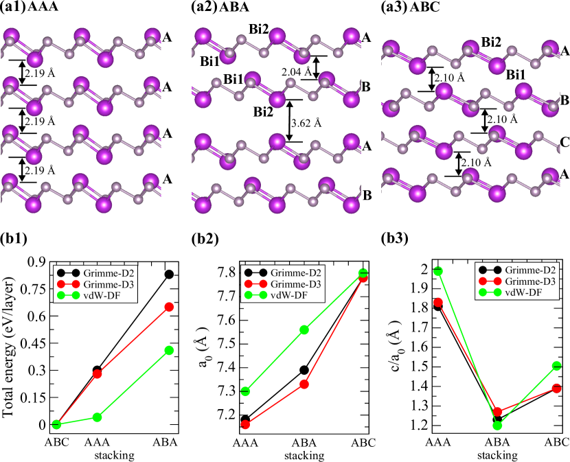
We initially investigated the structural properties to acquire a comprehensive understanding of BiP3-bulk in AAA-, ABA-, and ABC-stacked layers. We verified that the ABC-stacking [Fig. 1-(a1)] showed the lowest total energy considering semi- and non-local van der Waals potentials [Fig. A1-(b1) in Appendix-A].
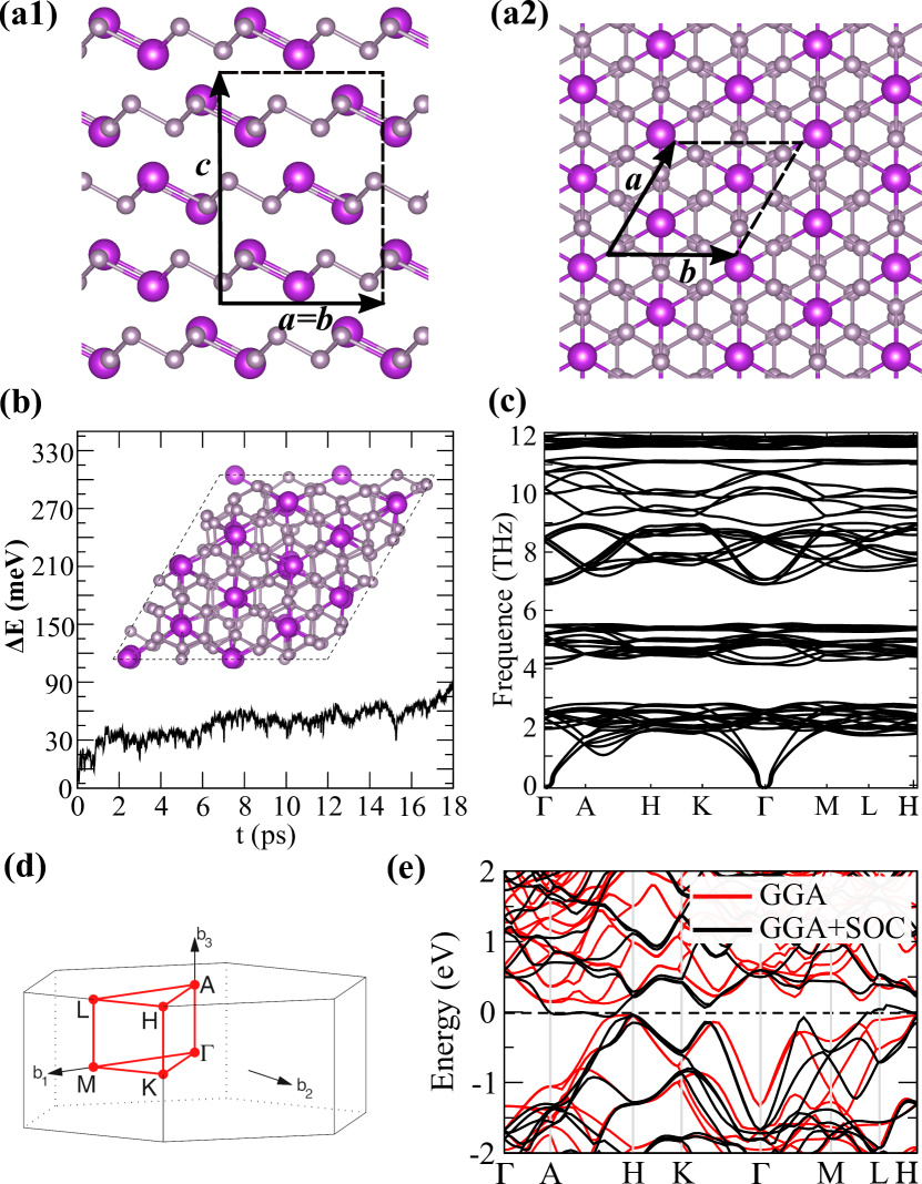
This is due to the strong electrostatic interaction between the positively charged bismuth and negatively charged phosphorus ions in the adjacent layers. In the ABC-stacking configuration, each phosphorus atom has a bismuth atom directly above and below it, forming a triangular lattice. This leads to the formation of a stable crystal structure with strong interlayer bonding, resulting in a lower total energy of the material. The AAA- and ABA-stacking configurations have weaker interlayer bonding (or a strong repulsion between layers) due to the lack of a triangular lattice and a different arrangement of bismuth and phosphorus atoms, resulting in higher total energy states. For consistency, we used the DFT-D2 method of Grimme for all analyses in this work, as the lattice parameters, atomic and interlayers distances were found to be similar for all admitted Vdw corrections, as shown in figure Fig. A1-(b1) of Appendix-A. Each bismuth (Bi) atom has three bonds with neighboring phosphorus (P) atoms. The crystal structure of the BiP3-bulk is characterized by a lattice with parameters = 7.83 Å [Fig. 1-(a2)], and = 1.34 Å, where refers to the parameter perpendicular to each single layer, which gives rise to a rhombohedral lattice system. This system is identified as belonging to the trigonal crystal symmetry, with lattice described by the crystallographic symbol R3 and point group 3. The lattice parameters indicate that the material has a hexagonal unit supercell with a threefold axis of symmetry. Additionally, the values of = = 90°, and = 120° show that the crystal structure possesses a threefold rotation axis and three perpendicular mirror planes. In ABC-stacking, the distance between two adjacent layers is 2.10 Å. The interatomic distance analysis of BiP3 reveals that the separation between phosphorus and bismuth atoms is approximately dBi-P = 2.78 Å. In contrast, the distance between P and P is around =2.24 Å. In addition to examining the ABC stacking, we conducted a comprehensive analysis of the AAA and ABA stackings of BiP3-bulk. An in-depth understanding of these structural analyses can be found in Appendix-A of the Supplementary Material.
In our study, we also conducted phonon dispersion analysis [Fig. 1-(b)] to investigate the vibrational properties of BiP3-bulk. The results of our analysis revealed that there were no negative frequencies, indicating that the bulk structure is stable and free from any imaginary modes of vibration. We also analyzed the dynamics and thermodynamic stability of BiP3 using AIMD [Fig. 1-(c)]. The findings show that the bulk structure is stable at room temperature and remained unchanged for 18 ps with minimal energy change results. Based on the result, it can be concluded that the arrangement of BiP3-bulk in an ABC stacking configuration is stable.
III.2 Electronic properties
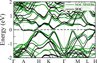
To investigate the electronic properties of BiP3 bulk, the initial step involved the computation of the electronic structure of the bulk phase without considering the effect of spin-orbit coupling (SOC), which revealed a semiconductor behavior characterized by an indirect bandgap of 0.17 eV [red lines in Fig. 1-[(d)]. However, High-resolution ARPES experiments have recently been conducted to analyze the surface and bulk bands of Bi, and the results strongly indicate the existence of nontrivial band topology in pure Bi[41, 42, 43]. Subsequently, the SOC was incorporated into the calculation, and the resulting electronic structure of the BiP3 system became metallic [black lines in Fig. 1-[(d)]. The SOC coupling in BiP3-bulk creates electronic connectivity between layers. This is evident along the -H and M-H directions, where the electronic properties turn metallic, indicating significant modifications to interlayer interactions. Furthermore, the HSE06 energy dispersion (Fig. B2 in Appendix-B) reveals that the metallic states near the Fermi level in the bulk remain largely consistent, providing further validation for the theoretical findings.
IV BiP3 monolayer
We proceed with our investigation by admitting the structure properties of the m-BiP3, which has the trigonal symmetry group and a hexagonal honeycomb lattice characterized by a puckered atomic layer. By using phonon dispersion spectra, Such monolayers were previously confirmed by Yi-Yuan Wu et al.[44] and Hong-Yao Liu et al.[45]. We calculated the energy required to exfoliate one or two layers of BiP3, and our findings demonstrate applicable exfoliation energies of 1.07 and 0.96 J/ for monolayer and bilayer extraction from a six-layer (6L) BiP3 slab, respectively. The Appendix-C provides details on obtaining the exfoliation energy. These values are close to the cleavage energies of other triphosphides, e.g., GeP3 (1.14 J/) [30], InP3 (1.32 J/) [46], CaP3 (1.30 J/) [29], and SnP3 (0.57 J/) [28]. Regarding the structure, the Bi atom forms three Bi-P bonds with three adjacent P atoms, while the P atom forms one Bi-P bond and two P-P bonds. The lattice parameters for this monolayer are optimized with = = 7.11 Å [Fig. 2-(a1)]. Compared to the BiP3-bulk, the relaxation process of the m-BiP3 resulted in a significant reduction of approximately 9% in the in-plane lattice parameters and , leading to a more pronounced puckered structure characterized by a larger value (=1.26 Å =1.55 Å)[Fig. 2-(a2)]. However, the bonding distances between atoms remained unchanged.
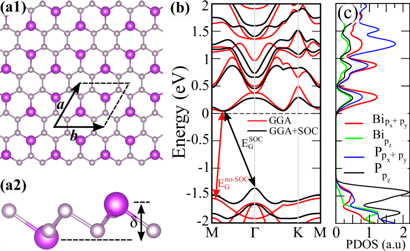
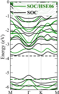
Additionally, we have found that m-BiP3 has a band structure with an indirect gap of 1.55 eV [Fig. 2-(b)]. The electronic properties of m-BiP3 are greatly affected by SOC. The band structure between non-SOC and SOC calculations shows significant differences, with the SOC-induced spin splitting of the bands resulting in a smaller indirect gap in the SOC calculation than in the no-SOC ( 1.55 eV 1.40 eV). The valence band maximum (VBM) is at the center of the Brillouin zone, specifically at the point, while the conduction band minimum (CBM) lies between the and M high symmetry points. Additionally, the bands exhibit anisotropic behavior, which varies depending on the crystal momentum direction. Hence, SOC plays a crucial role in comprehending the electronic structure and transport properties of m-BiP3. It is interesting to note that Hong-Yao Liu et al. [45] did not consider SOC in their calculations, yet they observed that the gap energy and parabolic behavior around the point were similar to those obtained from SOC calculations. This implies that the electronic properties of m-BiP3 may not be solely influenced by SOC, and other factors such as crystal structure and chemical bonding must also have an impact. Additionally, we utilized a hybrid functional approach (GGA+SOC+HSE06) to further investigate the electronic properties of m-BiP3, and we found out that the band gap increased from 1.40 eV to 2.00 eV [Fig. D4 in Appendix-D]. Moreover, the VBM and CBM experienced similar shifts down and up due to the HSE06’s inclusion concerning the pure SOC calculation. Notably, despite these alterations, the dispersion and band indirect gap were quite preserved. Based on the partial density of states (pDOS) obtained from the SOC+HSE06 calculation, it can be inferred that the states near the Fermi level are primarily derived from P orbitals in the vVBM, and Bi and P orbitals in the CBM [Fig. 2-(c)].
V BiP3 few layers
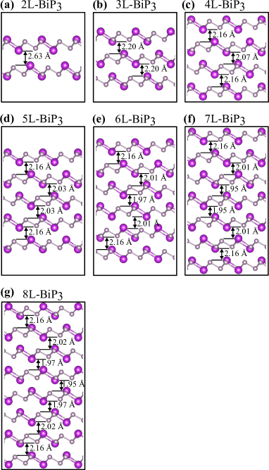
We thoroughly investigated the electronic and structural characteristics of BiP3 with few layers [Fig. , ranging from two (2L) [Fig. E5-(a) in Appendix-E] to eight layers (8L) [Fig. E5-(g) in Appendix-E] . We have considered AB-stacking for the bilayer. From 3L onwards, the layers follow ABC stacking. Our analysis of the structural properties revealed exciting trends in the evolution of the lattice parameter from the monolayer to multilayer regimes. We noticed that as the layer count increased from a monolayer (7.11 Å) to eight layers (7.43 Å), the lattice parameter grew consistently, indicating a gradual convergence towards the lattice parameter of the bulk material (7.83 Å), as can be seen in the Table-1. Additionally, it has been observed that the interlayer separation diminishes as the number of layers comprising the material increases. In the context of a bilayer configuration, the interlayer equilibrium separation is 2.63 Å. However, as the number of layers increases from 3L to 8L, the interlayer distance adjacent to the surface’s edges measures approximately 2.17 Å, whereas towards the central region of the surface, the interlayer separation contracts to an approximate value of 2.00 Å. This distinctive behavior is attributed to the amplification of van der Waals forces between neighboring layers as the layer count ascends, consequently compelling them to draw closer together. Furthermore, as the stacking arrangement increases, the distance between layers decreases, approaching the bulk configuration of BiP3. In the BiP3-bulk, the interlayer distance is quantified at around 2.10 Å. This tendency is explained by the denser packing of layers, leading to an interlayer spacing close to the BiP3’s bulk form.
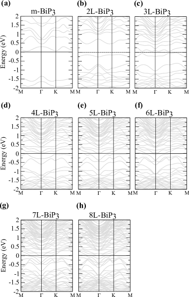
Regarding the electronic properties of a few layers, we noticed that the characteristics of BiP3 changed as the number of layers is altered, as shown by the band gaps values compiled in Table-1. The energy gap has decreased from 1L to 4L, suggesting a shift towards the metallic electronic behavior of the bulk. The metallic state was verified in configurations of five layers or more (5L, 6L, 7L, and 8L). Details on the band structures of BiP3 from 2L to 8L can be seen in Fig.F6 of Appendix-F.
| Layers | a0(Å) | Band gap (eV) |
|---|---|---|
| 1 | 7.11 | 1.40 |
| 2 | 7.17 | 0.60 |
| 3 | 7.32 | 0.08 |
| 4 | 7.36 | 0.06 |
| 5 | 7.39 | metallic |
| 6 | 7.40 | metallic |
| 7 | 7.41 | metallic |
| 8 | 7.43 | metallic |
| 7.83 | metallic |
VI Graphene/BiP3 heterostructure
We now investigate the electronic and structural properties of the vdW heterostructure formed by the deposition of a single layer of graphene (G) on top of the BiP3 monolayer (G/m-BiP3). The simulation supercell consists of a () graphene and a () BiP3 cells. The pristine primitive graphene cell has a lattice parameter of Å, resulting in a lattice mismatch of with the m-BiP3. As the m-BiP3 band gap is sensitive to applied strains, we choose to fix the m-BiP3 lattice parameters, hence compressing the graphene layer. We have considered three highly symmetric configurations for depositing the G-layer on top of the m-BiP3, as presented in Fig.G7 of Appendix-G. For each arrangement, we calculate the binding energy () using the following equation:
| (1) |
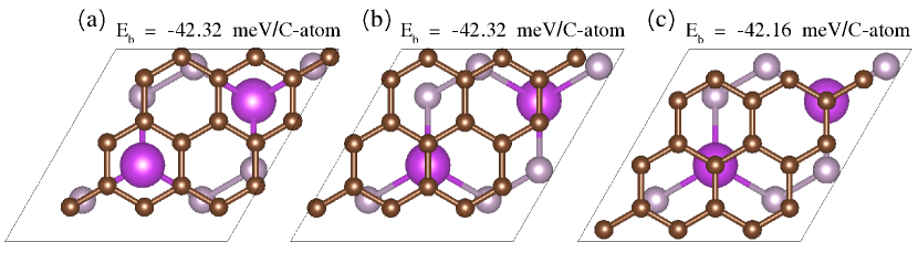
where , , and represent the total energies of the G/m-BiP3 junction, pristine G, and pristine m-BiP3, respectively. is the number of carbon atoms in the G layer. We find that the process is exothermic for all simulated configurations with a similar value, with a maximum difference of only about 1% between them. The most energetically stable stacking configuration presents the hole of the graphene hexagonal rings on top of the upmost Bi of the BiP3, with meV/C-atom, which is shown in Fig. 3(a). One can typically find this order in graphene vdW heterostructures [32, 14]. The interlayer distance between G and m-BiP3 [see Fig. 3(a)] in the equilibrium geometry is 3.35 Å, which suggests that there are no chemical bonds between them. Furthermore, the structural properties of both G and m-BiP3 remain unaffected as they are brought closer, indicating that weak vdW forces govern the interactions between G and m-BiP3.
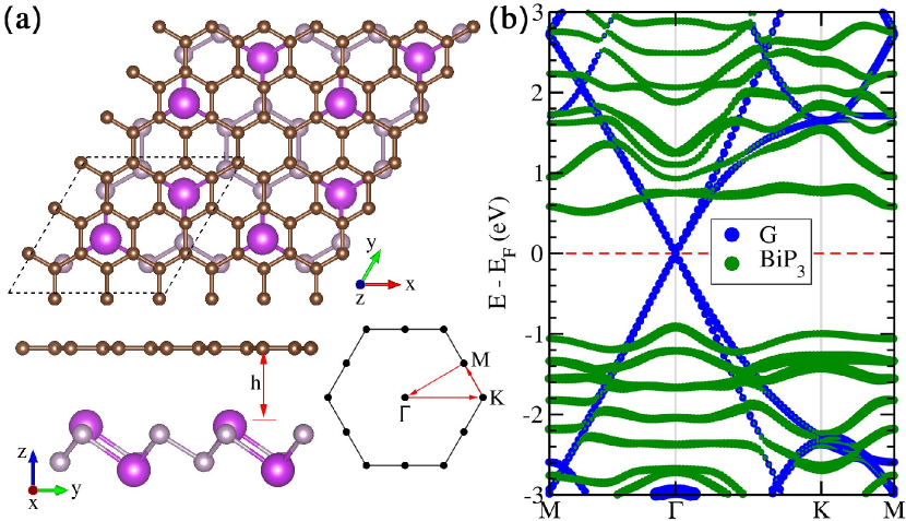
We then proceed to examine the electronic characteristics of the G/m-BiP3 vdW heterostructure. As demonstrated earlier, including SOC is crucial for describing the electronic structure of m-BiP3. Therefore, SOC is taken into account for all G/m-BiP3 electronic analyses. Fig. 3(b) displays the projected band structure, which reveals the presence of the graphene linear Dirac-like dispersion relation around the Fermi level. The m-BiP3 layer retains its semiconductor properties from the pristine monolayer, with an indirect energy gap of 1.42 eV between the VBM and CBM, which is 20 eV larger than the isolated m-BiP3 band gap. This increase in the band gap might be attributed to the weak interaction between m-BiP3 and the G layer. These results demonstrate that the electronic properties of isolated G and m-BiP3 layers are well-preserved in the G/m-BiP3 heterostructure formation, indicating a small degree of interaction at the interface.
Recently, weak interactions in certain 2D van der Waals (vdW) heterostructures have been investigated to design metal-semiconductor junctions with low chemical bond formation, chemical disorder, and defect density. In such scenarios, the Schottky-Mott rule proves useful for estimating the Schottky barrier height (SBH) of the system.[47] The weak Fermi level pinning on metal-2D semiconductor vdW junctions allows the tuning of the SBH through the metal working function () modulation.[48, 49] As shown in Fig. 4(a), we find a work function eV for the free-standing graphene, in agreement with previous theoretical and experimental works. [50, 51, 52] Moreover, the isolated m-BiP3 CBM and VBM energy values are informed in Fig. 4(a). Taking the vacuum energy () as a reference, we note that the graphene Dirac cone lies between those values. The G/m-BiP3 band structure [Fig. 3(a)] suggests the absence (or very minimal) of Fermi level pinning at the junction. This observation suggests that the Schottky-Mott rule can be employed to determine the SBH in the G/m-BiP3 heterostructure. Thus, we define a -type SBH () as the difference between the m-BiP3 CBM energy and the graphene Fermi level: . Similarly, the -type SBH is defined as , where represents the VBM energy. These definitions yield , where denotes the energy gap of m-BiP3. For the equilibrium system, we find eV and eV, as illustrated in Fig. 4(a). Since the graphene Dirac cone lies closer to the m-BiP3 CBM than its VBM energy level, the G/m-BiP3 heterostructure constitutes a -type Schottky contact, with electron conduction prevailing within the system.
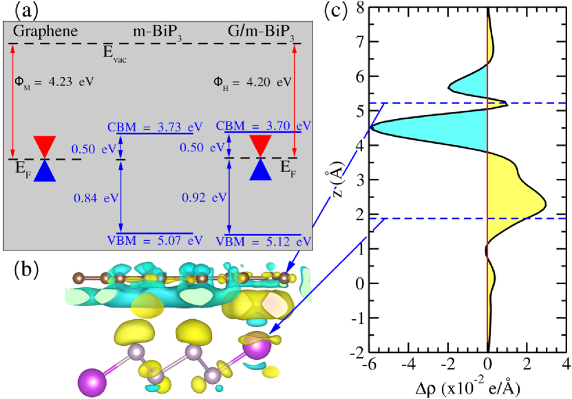
In Fig. 4(b) we plot differential charge density, defined as
| (2) |
where represents the electronic density for the heterostructure, corresponds to pristine G, and represents isolated m-BiP3. The obtained results reveal a charge depletion in the graphene region (blue isosurfaces), accompanied by an accumulation of charge on the m-BiP3 surface (yellow isosurfaces). To further investigate the redistribution of charge within the system, we also calculate the integral of the differential charge density (DCD) over the -plane using the following equation:
| (3) |
where represents the integrated DCD, and S denotes the surface area of the supercell. The outcome of this calculation is depicted in Fig. 4(c), clearly illustrating the observed electronic charge accumulation on graphene and depletion on m-BiP3. By employing the Bader charge analysis method [53, 54], we verified an increase of 0.033 ( /cm2) in the G layer, coming from the m-BiP3. The small amount of charge transfer suggests the formation of weak vdW interactions at the heterojunction interface.
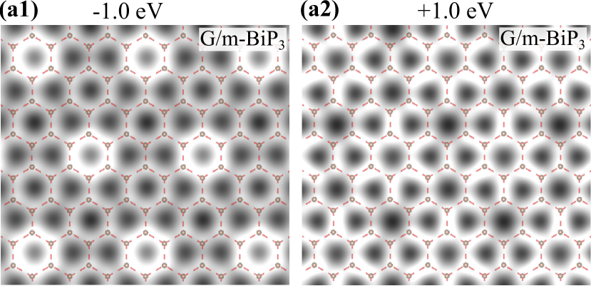
Utilizing the theoretical Tersoff-Hamann method[55], Scanning Tunneling Microscopy (STM) simulations were conducted to investigate the atomic-scale features within the G/m-BiP3 system. STM images were obtained at energy levels corresponding to E 1.0 eV, yielding the following observations: (i) the absence of a hexagonal pattern in both occupied [Fig.5-(a)] and empty [Fig.5-(b)] states suggest an interaction between the graphene layer and m-BiP3, deviating from the pristine graphene’s expected hexagonal symmetry; (ii) bright spots observed in both empty and occupied states stem from specific interactions between the topmost bismuth of m-BiP3 and carbon atoms within the graphene layer, indicating prominent features in the STM images originate from this Bi-C interaction (in agreement with differential charge density in Fig.4-(b)); (iii) in occupied states, bright states result from the hybridization between Bi and C orbitals. This hybridization is similarly observed in unoccupied states.
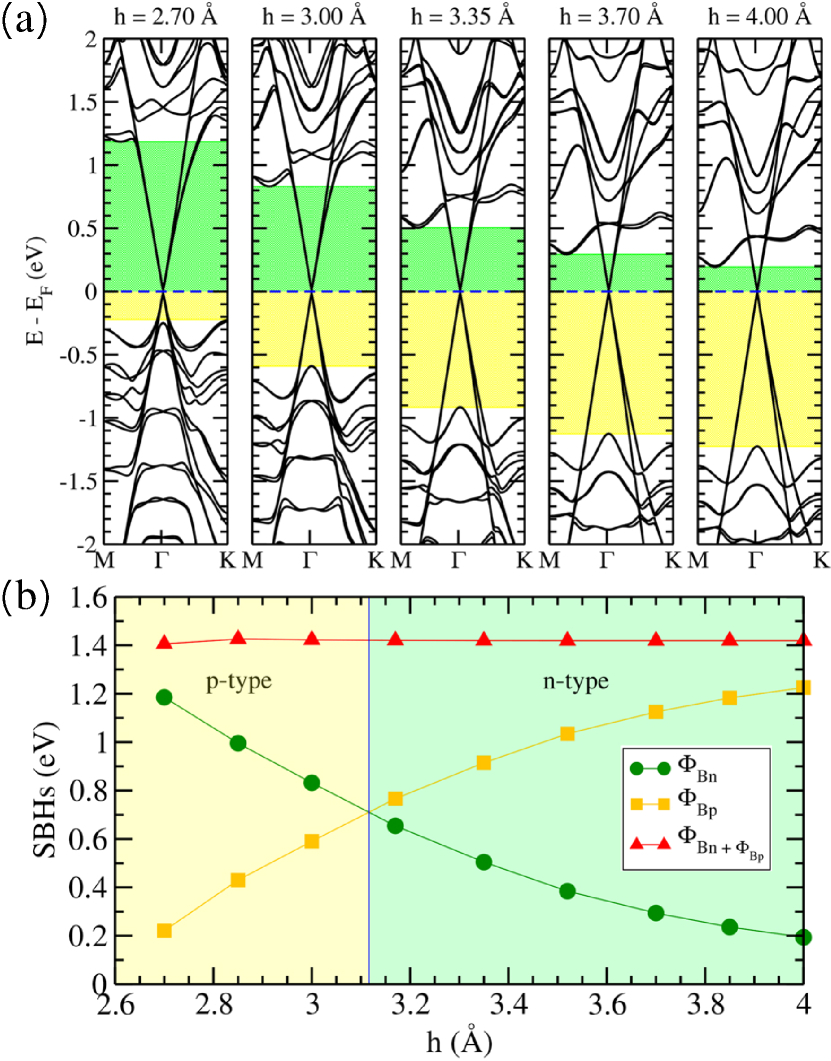
Enhancing the performance of metal-2D semiconductor vdW contacts in electronic devices has posed a significant challenge, primarily due to the difficulty in controlling the SBH. To address this, researchers have explored various approaches, including adjusting the SBH through interlayer coupling modulation. In our system, this can be accomplished by modulating the interlayer distance () between the G layer and the topmost atomic layer of m-BiP3. To examine the impact of modifying on the electronic properties of G/m-BiP3, we computed the band structure for various interlayer distances, as depicted in Fig. 6(a). As the interlayer distance increases from Å, the graphene Dirac cone gradually shifts towards the CBM of the m-BiP3, while the CT decreases from . Consequently, this leads to a decrease in and an increase in . On the other hand, when reducing from 3.35 to 3.00 Å () and further to 2.70 Å (), there is an observed increase in and a corresponding decrease in . In Fig. 6(b), we present the SBHs for different interlayer distances. As the interlayer distance () increases from its equilibrium value, the value increases, while decreases. Conversely, when the interlayer distance is decreased from its equilibrium value, an opposite trend is observed. At Å, and become close to each other, and below this point, the magnitudes of the SBHs are inverted, meaning becomes smaller than . Consequently, by adjusting the interlayer distance, a transition from -type to -type Schottky contact can be induced in the G/m-BiP3 heterostructure. Throughout the process of varying , the energy gap between the m-BiP3 VBM and CBM remains nearly constant, as indicated by the red triangles in Fig. 6(b).
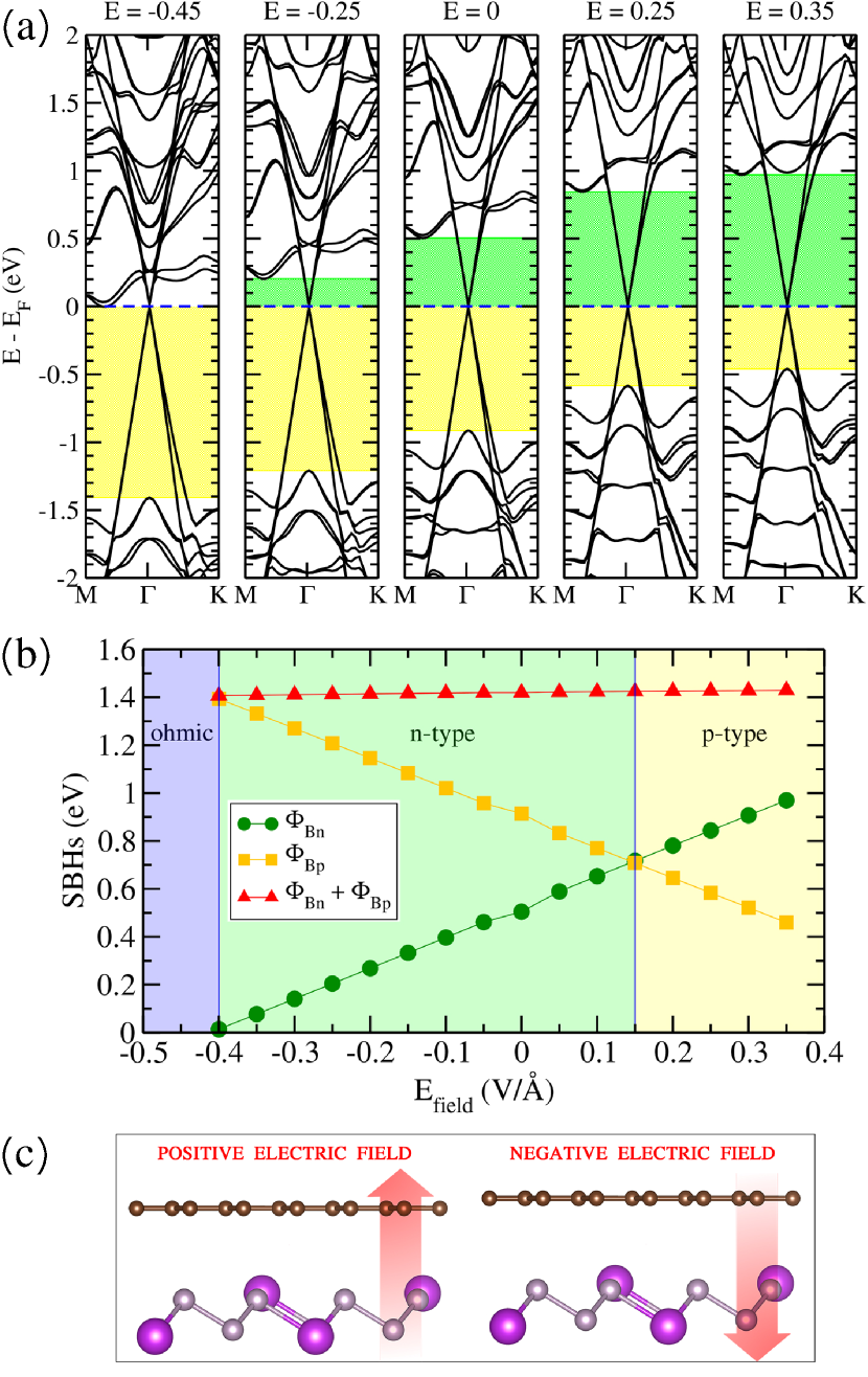
Applying a perpendicular external electric field () is another commonly employed method to modify the SBHs in G vdW heterostructures. The external transverse electric field values in our calculations range from -0.45 to 0.35 V/Å. The positive direction of the electric field points from BiP3 to graphene, whereas the negative direction points in the opposite direction, as seen in Fig. 7(c). Consequently, we investigate the impact of the electric gating on the electronic properties of the G/m-BiP3 heterostructure in Fig. 7(a) we present the band structure for selected values. For positive values ( and V/Å), we observe an increase in and a decrease in . On the other hand, for V/Å decreases and increases. At V/Å, although continues to increase, a conduction band crosses the Fermi level, forming an ohmic contact.
Fig. 7(b) shows the computed SBHs for different values of . Positive values of lead to an increase in the while decreases, both exhibiting a linear relationship. When approaches 0.15 V/Å, approximately equals , and beyond this threshold the system manifests a -type Schottky contact. Consequently, we successfully induce a transition from -type to -type Schottky contact in G/m-BiP3 by applying a perpendicular positive to the system. Despite the G Fermi level shifting closer to the m-BiP3 VBM, no intersection between the m-BiP3 VBM and the system Fermi level is observed, even at the highest applied value ( V/Å). As a result, no formation of a -type Ohmic contact occurs within the range of applied . Upon reversing the polarity of , the SBHs exhibit an opposite trend, increasing the separation distance between and , thus the system remains with a -type Schottky contact. For values below V/Å the CBM crosses the Fermi energy, resulting in a -type ohmic contact. The nearly constant line formed by red triangles indicates that the energy gap between the VBM and CBM of the material remains unaltered in the range of applied .
VII Summary and Conclusions
In conclusion, the structural and electronic properties of the bulk and layered forms of the BiP3 triphosphide have been investigated by first-principles calculations. Phonon spectra and molecular dynamics simulations confirm that the 3D crystal of BiP3 is a metal thermodynamically stable with no bandgap. Notably, few BiP3 layers exhibit semiconductor properties only with one to four layers but behave like a metal, similar to the bulk with more than five layers. By changing the number of layers, the electronic properties of BiP3 triphosphide can be fine-tuned, making it suitable for technological applications. Based on this, the electronic properties of the G/m-BiP3 van der Waals heterostructure were examined. Applying vertical strain and an external electric field can adjust the electronic properties of the G/m-BiP3 heterostructure, according to our calculations. Thus, we show that few-layers BiP3 is an interesting material for realizing nanoelectronic and optoelectronic devices and is an excellent option for designing Schottky nanoelectronic devices.
Acknowledgements.
The authors acknowledge financial support from the Brazilian agencies CNPq, CAPES, FAPEMIG, and INCT-Nanomateriais de Carbono, and the LCC-UFLA, CENAPAD-SP and Laboratório Nacional de Computação Científica (LNCC-SCAFMat2) for computer time.References
- Geim [2009] A. K. Geim, Graphene: Status and prospects, Science 324, 1530 (2009).
- Nair et al. [2012] R. R. Nair, H. A. Wu, P. N. Jayaram, I. V. Grigorieva, and A. K. Geim, Unimpeded permeation of water through helium-leak tight graphene-based membranes, Science 335, 442 (2012).
- Novoselov et al. [2012] K. S. Novoselov, V. I. Falko, L. Colombo, P. R. Gellert, M. G. Schwab, and K. Kim, A roadmap for graphene, Nature 490, 192 (2012).
- Chen et al. [2008] H. Chen, M. B. Müller, K. J. Gilmore, G. G. Wallace, and D. Li, Mechanically strong, electrically conductive, and biocompatible graphene paper, Advanced Materials 20, 3557 (2008).
- Balandin et al. [2008] A. A. Balandin, S. Ghosh, W. Bao, I. Calizo, D. Teweldebrhan, F. Miao, and C. N. Lau, Superior thermal conductivity of single-layer graphene, Nano Letters 8, 902 (2008).
- Biswas and Lee [2011] C. Biswas and Y. H. Lee, Graphene versus carbon nanotubes in electronic devices, Advanced Functional Materials 21, 3806 (2011).
- Avouris [2010] P. Avouris, Graphene: Electronic and photonic properties and devices, Nano Letters 10, 4285 (2010).
- Han et al. [2017] T.-H. Han, H. Kim, S.-J. Kwon, and T.-W. Lee, Graphene-based flexible electronic devices, Materials Science and Engineering: R: Reports 118, 1 (2017).
- Raccichini et al. [2015] R. Raccichini, A. Varzi, S. Passerini, and B. Scrosati, The role of graphene for electrochemical energy storage, Nature Materials 14, 271 (2015).
- Chen et al. [2015] Y. Chen, C. Tan, H. Zhang, and L. Wang, Two-dimensional graphene analogues for biomedical applications, Chem. Soc. Rev. 44, 2681 (2015).
- Dean et al. [2012] C. Dean, A. Young, L. Wang, I. Meric, G.-H. Lee, K. Watanabe, T. Taniguchi, K. Shepard, P. Kim, and J. Hone, Graphene based heterostructures, Solid State Communications 152, 1275 (2012), exploring Graphene, Recent Research Advances.
- Iqbal and Rehman [2018] M. Z. Iqbal and A.-U. Rehman, Recent progress in graphene incorporated solar cell devices, Solar Energy 169, 634 (2018).
- Jo et al. [2012] G. Jo, M. Choe, S. Lee, W. Park, Y. H. Kahng, and T. Lee, The application of graphene as electrodes in electrical and optical devices, Nanotechnology 23, 112001 (2012).
- de Andrade Deus and de Oliveira [2020] D. P. de Andrade Deus and I. S. S. de Oliveira, Tuning the schottky barrier height in graphene/monolayer-gei2 van der waals heterostructure, Journal of Physics: Condensed Matter 32, 355501 (2020).
- Di Bartolomeo [2016] A. Di Bartolomeo, Graphene schottky diodes: An experimental review of the rectifying graphene/semiconductor heterojunction, Physics Reports 606, 1 (2016), graphene Schottky diodes: An experimental review of the rectifying graphene/semiconductor heterojunction.
- Wang and Yu [2016] H. Wang and G. Yu, Direct cvd graphene growth on semiconductors and dielectrics for transfer-free device fabrication, Advanced Materials 28, 4956 (2016).
- Yankowitz et al. [2019] M. Yankowitz, Q. Ma, P. Jarillo-Herrero, and B. J. LeRoy, van der waals heterostructures combining graphene and hexagonal boron nitride, Nature Reviews Physics 1, 112 (2019).
- Wang et al. [2017] J. Wang, F. Ma, and M. Sun, Graphene, hexagonal boron nitride, and their heterostructures: properties and applications, RSC Adv. 7, 16801 (2017).
- [19] H. Wang, H. Feng, and J. Li, Graphene and graphene-like layered transition metal dichalcogenides in energy conversion and storage, Small 10, 2165.
- Joshi et al. [2018] N. Joshi, T. Hayasaka, Y. Liu, H. Liu, O. N. Oliveira, and L. Lin, A review on chemiresistive room temperature gas sensors based on metal oxide nanostructures, graphene and 2d transition metal dichalcogenides, Microchimica Acta 185, 213 (2018).
- Garcia et al. [2018] J. H. Garcia, M. Vila, A. W. Cummings, and S. Roche, Spin transport in graphene/transition metal dichalcogenide heterostructures, Chem. Soc. Rev. 47, 3359 (2018).
- tri [1972] The crystal structure of snp3 and a note on the crystal structure of gep3, Journal of Solid State Chemistry 5, 441 (1972).
- Yao et al. [2019] S. Yao, X. Zhang, Z. Zhang, A. Chen, and Z. Zhou, 2d triphosphides: Sbp3 and gap3 monolayer as promising photocatalysts for water splitting, International Journal of Hydrogen Energy 44, 5948 (2019).
- Donohue and Young [1970] P. Donohue and H. Young, Synthesis, structure, and superconductivity of new high pressure phases in the systems gep and geas, Journal of Solid State Chemistry 1, 143 (1970).
- Kinomura et al. [1983] N. Kinomura, K. Terao, S. Kikkawa, H. Horiuchi, M. Koizumi, and H. Setoguchi, Synthesis and crystal structure of inp3, Materials Research Bulletin 18, 53 (1983).
- Shojaei and Kang [2017] F. Shojaei and H. S. Kang, Partially planar bp3 with high electron mobility as a phosphorene analog, J. Mater. Chem. C 5, 11267 (2017).
- Ghosh et al. [2018] B. Ghosh, S. Puri, A. Agarwal, and S. Bhowmick, Snp3: A previously unexplored two-dimensional material, The Journal of Physical Chemistry C 122, 18185 (2018).
- Sun et al. [2018] S. Sun, F. Meng, H. Wang, H. Wang, and Y. Ni, Novel two-dimensional semiconductor snp3: high stability, tunable bandgaps and high carrier mobility explored using first-principles calculations, J. Mater. Chem. A 6, 11890 (2018).
- Lu et al. [2018] N. Lu, Z. Zhuo, H. Guo, P. Wu, W. Fa, X. Wu, and X. C. Zeng, Cap3: A new two-dimensional functional material with desirable band gap and ultrahigh carrier mobility, The Journal of Physical Chemistry Letters 9, 1728 (2018).
- Jing et al. [2017] Y. Jing, Y. Ma, Y. Li, and T. Heine, Gep3: A small indirect band gap 2d crystal with high carrier mobility and strong interlayer quantum confinement, Nano Letters 17, 1833 (2017).
- de A. Deus et al. [2021] D. P. de A. Deus, I. S. S. de Oliveira, J. a. B. Oliveira, W. a. L. Scopel, and R. H. Miwa, Magnetic switch and electronic properties in chromium-intercalated two-dimensional , Phys. Rev. Mater. 5, 054002 (2021).
- Zhang and Hu [2021] D. Zhang and Y. Hu, Tunable schottky contact in graphene/inp3 van der waals heterostructures, Applied Surface Science 554, 149608 (2021).
- Slassi et al. [2020] A. Slassi, P. Sorokin, and A. Pershin, Ohmic/schottky barrier engineering in metal/snp3 heterostructures, Journal of Alloys and Compounds 831, 154800 (2020).
- Zhang et al. [2019] C. Zhang, G. Yu, R. Ku, X. Huang, and W. Chen, Theoretical investigation on the high her catalytic activity of 2d layered gep3 nanomaterials and its further enhancement by applying the surface strain or coupling with graphene, Applied Surface Science 481, 272 (2019).
- Perdew et al. [1996] J. P. Perdew, K. Burke, and M. Ernzerhof, Generalized gradient approximation made simple, Phys. Rev. Lett. 77, 3865 (1996).
- Blöchl [1994] P. E. Blöchl, Projector augmented-wave method, Phys. Rev. B 50, 17953 (1994).
- Kresse and Furthmüller [1996] G. Kresse and J. Furthmüller, Efficiency of ab-initio total energy calculations for metals and semiconductors using a plane-wave basis set, Computational Materials Science 6, 15 (1996).
- Grimme [2004] S. Grimme, Accurate description of van der waals complexes by density functional theory including empirical corrections, Journal of Computational Chemistry 25, 1463 (2004).
- Monkhorst and Pack [1976] H. J. Monkhorst and J. D. Pack, Special points for brillouin-zone integrations, Phys. Rev. B 13, 5188 (1976).
- Togo and Tanaka [2015] A. Togo and I. Tanaka, First principles phonon calculations in materials science, Scripta Materialia 108, 1 (2015).
- Ohtsubo et al. [2013] Y. Ohtsubo, L. Perfetti, M. O. Goerbig, P. L. Fèvre, F. Bertran, and A. Taleb-Ibrahimi, Non-trivial surface-band dispersion on bi(111), New Journal of Physics 15, 033041 (2013).
- Perfetti et al. [2015] L. Perfetti, J. Faure, E. Papalazarou, J. Mauchain, M. Marsi, M. Goerbig, A. Taleb-Ibrahimi, and Y. Ohtsubo, New aspects of electronic excitations at the bismuth surface: Topology, thermalization and coupling to coherent phonons, Journal of Electron Spectroscopy and Related Phenomena 201, 60 (2015), special issue on electron spectroscopy for Rashba spin-orbit interaction.
- Ito et al. [2016] S. Ito, B. Feng, M. Arita, A. Takayama, R.-Y. Liu, T. Someya, W.-C. Chen, T. Iimori, H. Namatame, M. Taniguchi, C.-M. Cheng, S.-J. Tang, F. Komori, K. Kobayashi, T.-C. Chiang, and I. Matsuda, Proving nontrivial topology of pure bismuth by quantum confinement, Phys. Rev. Lett. 117, 236402 (2016).
- Wu et al. [2021] Y.-Y. Wu, Q. Wei, J. Zou, and H. Yang, Ultra-low thermal conductivity and high thermoelectric performance of monolayer bip3: a first principles study, Phys. Chem. Chem. Phys. 23, 19834 (2021).
- Liu et al. [2020] H.-Y. Liu, C.-L. Yang, M.-S. Wang, and X.-G. Ma, Two-dimensional bip3 with high carrier mobility and moderate band gap for hydrogen generation from water splitting, Applied Surface Science 501, 144263 (2020).
- Jalil et al. [2020] A. Jalil, Z. Zhuo, Z. Sun, F. Wu, C. Wang, and X. Wu, A phosphorene-like inp3 monolayer: structure, stability, and catalytic properties toward the hydrogen evolution reaction, J. Mater. Chem. A 8, 1307 (2020).
- Liu et al. [2018] Y. Liu, J. Guo, E. Zhu, L. Liao, S.-J. Lee, M. Ding, I. Shakir, V. Gambin, Y. Huang, and X. Duan, Approaching the schottky-mott limit in van der waals metal-semiconductor junctions, Nature 557, 696 (2018).
- Padilha et al. [2015] J. E. Padilha, A. Fazzio, and A. J. R. da Silva, van der waals heterostructure of phosphorene and graphene: Tuning the schottky barrier and doping by electrostatic gating, Phys. Rev. Lett. 114, 066803 (2015).
- Liu et al. [2016] Y. Liu, P. Stradins, and S.-H. Wei, Van der waals metal-semiconductor junction: Weak fermi level pinning enables effective tuning of schottky barrier, Science Advances 2, 10.1126/sciadv.1600069 (2016).
- Yu et al. [2009] Y.-J. Yu, Y. Zhao, S. Ryu, L. E. Brus, K. S. Kim, and P. Kim, Tuning the graphene work function by electric field effect, Nano Letters 9, 3430 (2009), pMID: 19719145, https://doi.org/10.1021/nl901572a .
- Garg et al. [2014] R. Garg, N. K. Dutta, and N. Roy Choudhury, Work function engineering of graphene, Nanomaterials 4, 267 (2014).
- Leenaerts et al. [2016] O. Leenaerts, B. Partoens, F. Peeters, A. Volodin, and C. Van Haesendonck, The work function of few-layer graphene, Journal of Physics: Condensed Matter 29, 035003 (2016).
- Bader [1990] R. F. W. Bader, Atoms in Molecules - A Quantum Theory (Oxford University Press, Oxford, 1990).
- Henkelman et al. [2006] G. Henkelman, A. Arnaldsson, and H. Jónsson, Comput. Mater. Sci. 36, 254 (2006).
- Tersoff and Hamann [1985] J. Tersoff and D. R. Hamann, Phys. Rev. B 31, 805 (1985).
Appendix A Lattice parameters and energy stability
We investigate three possible high symmetry stacking layers named (i) AAA-stacking; there is no shift between the layers, and the atoms of one layer are precisely aligned with those of another [Fig. A1-(a1)]; (ii) ABA-stacking, BiP3-bulk is formed by stacking AB layers of BiP3 bilayers, where one bismuth (Bi1) in each bilayer is positioned above (or below) a hexagon formed by the phosphorus of the other layer, and the remaining bismuth (Bi2) is located in the rhombohedral spaces between the AB stacked layers [Fig.A1-(a2)], and (iii) ABC-stacking, each layer contains bismuth (Bi1) located at the center of a hexagon formed by P atoms from the adjacent layer, and there is another bismuth (Bi2) that creates a rhombohedral space between two stacked layers [Fig.A1-(a3)]. We also have analyzed the total energy, lattice parameter (), and ratio for each stacking configuration [Fig. A1-(b1)-(b3)]. The comparison of different stacking arrangements shows that AAA-stacking maintains consistent interlayer distances of 2.19Å within the bulk structure. However, ABA-stacking experiences a significant increase in the interlayer distance along the B-A spacing, which reaches 3.62Å, due to the strong repulsion between Bi atoms. In contrast, ABC-stacking shows remarkable stability with an interlayer distance of 2.10Å, highlighting low repulsion and significant van der Waals interactions.
Appendix B SOC+HSE band structure of BiP3 bulk
This study evaluated the gap energy of BiP3-bulk [Fig. B2] using the Herd-Scuseria-Emzerhof hybrid functional (HSE06) calculation, employing a 10101 k-point mesh. We observed that adding HSE06 (green lines) did not change the metallic behavior. The band structures were similar to SOC+GGA (black lines).
Appendix C Exfoliaton energy to mono- and bilayer of BiP3
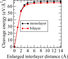
We compared the energy of a thick slab composed of six atomic layers of BiP3 (6L) to that of a single (two) atomic layer far away from the 5L (4L) slab. Our aim was to calculate the exfoliation energy. We achieved this by using a large supercell that could hold 6L-BiP3 while maintaining enough vacuum to prevent any interaction between its images. To simulate the mechanical exfoliation process, We isolated one or two atomic layers from the slab. We identified the point of stabilization of total energy to determine exfoliation energy. The energy needed for exfoliating a monolayer is 67 meV/Å2 (black line in Fig. C3), whereas for a bilayer, it is 60 meV/Å2 (red line in Fig. C3).
Appendix D SOC+HSE band structure of m-BiP3
Appendix E Structural models of few m-BiP3 layers
Appendix F Band structure of few m-BiP3 layers
Appendix G Graphene/BiP3stacking configurations
We have examined three highly symmetric configurations of the heterostructure formed by graphene on BiP3, with the topmost Bi atom placed in three distinct positions: (i) at the center of a carbon hexagon [Fig. G7-(a)], (ii) on a carbon bridge [Fig. G7-(b)], and aligned with the carbon atoms in graphene [Fig. G7-(c)]. Our analysis reveals that the most stable configuration, with the topmost Bi atom positioned in the center of a carbon hexagon, exhibits greater stability when evaluated using the vdW-DF and Grimme’s DFT-D2 and DFT-D3 approaches. However, it’s worth noting that the differences in stability between this configuration and the other two are marginal, with the less stable configurations showing less than a 1% difference in the binding energy.