Electron surface scattering kernel for a plasma facing a semiconductor
Abstract
Employing the invariant embedding principle for the electron backscattering function, we present a strategy for constructing an electron surface scattering kernel to be used in the boundary condition for the electron Boltzmann equation of a plasma facing a semiconducting solid. It takes the microphysics responsible for electron emission and backscattering from the interface into account. To illustrate the approach, we consider silicon and germanium, describing the interface potential by an image-step and impact ionization across the energy gap as well as scattering on phonons and ion cores by a randium-jellium model. The emission yields deduced from the kernel agree sufficiently well with measured data, despite the simplicity of the model, to support its use in the boundary condition of the plasma’s electron Boltzmann equation.
pacs:
68.49.Jk, 79.20.Hx, 52.40.HfI Introduction
Man-made plasmas are bounded by condensed matter. Essentially all commercially exploited technological plasmas Weltmann et al. (2019) interact with either a liquid or a solid. For instance, plasmas for medical applications naturally have contact with human cells and hence with a liquid environment, whereas plasmas used for surface modification or surface catalysis are in contact with solids. Solids and plasmas are especially strongly coupled in semiconductor-based microdischarges R. Michaud and V. Felix and A. Stolz and O. Aubry and P. Lefaucheux and S. Dzikowski and V. Schulz-von der Gathen and L. J. Overzet and R. Dussart (2018); Eden et al. (2013); Dussart et al. (2010), where the surface to volume ratio is particularly large, making the interaction with the solid an integral part of the physical system. Even magnetically confined fusion plasmas interact with condensed matter in the divertor region via sheaths Campanell (2020); Tolias et al. (2020) and dust particles Vignitchouk et al. (2018); Tolias (2014), as do plasmas employed for electric propulsion in Hall thrusters Raitses et al. (2005); Dunaevsky et al. (2003).
Although not complete, the list indicates that a kinetic description of technological plasmas, based on equations for the electromagnetic fields and a set of Boltzmann equations for the various particle species, requires boundary conditions for the fields and the particle distribution functions. As in any Boltzmann-type modeling of kinetic phenomena M. M. R. Williams (1971); Kogan (1969); Al’pert et al. (1965), the latter is an integral relating at the boundary the distribution function of the outgoing particles with that of the incoming ones.
The kernel of this integral–the surface scattering kernel Cercignani (1995)–is a complicated object, because it arises from the microscopic processes at or within the bounding medium responsible for particle reflection and/or emission. Mathematical constraints enforced by the processes, such as positivity, normalization, and–in thermal equilibrium–reciprocity Kuscer (1971), can be straightforwardly formulated, but setting up an expression for the kernel, from which quantitative data can be deduced, requires to solve the kinetic problem also partly within the bounding medium. To avoid this task, phenomenological kernels Cercignani and Lampis (1971), containing a set of adjustable parameters, are widely used. For instance, a two-term scattering kernel, describing specular and diffuse reflection, has been employed in neutron transport M. M. R. Williams (1971), gas kinetics Kogan (1969), as well as plasma physics Al’pert et al. (1965). The electron boundary condition most popular in the modeling of technological low-temperature plasmas Becker et al. (2010); Loffhagen et al. (2002); Alves et al. (1997) even considers only specular reflection. It contains the electron reflection probability as an adjustable parameter.
Recently, however, an effort started to determine for plasma-exposed surfaces the electron reflection probability and the closely related secondary electron emission yield experimentally Schulze et al. (2022); Daksha et al. (2016); Demidov et al. (2015). The material dependence of the two parameters moves also more and more in the focus of a quantitative plasma modeling Daksha et al. (2019). It is thus appropriate to set up boundary conditions containing the wall’s microphysics more faithfully than the parameterized boundary conditions used so far.
The purpose of this work is to construct a physical boundary condition for the electron Boltzmann equation of a plasma in contact with a solid. To illustrate the approach, we consider a planar semiconducting plasma-solid interface, as it occurs in semiconductor-based microdischarges R. Michaud and V. Felix and A. Stolz and O. Aubry and P. Lefaucheux and S. Dzikowski and V. Schulz-von der Gathen and L. J. Overzet and R. Dussart (2018); Eden et al. (2013); Dussart et al. (2010). Instead of resolving the electron kinetics inside the solid by a separate Boltzmann equation, we employ the invariant embedding principle Dashen (1964); Glazov and Pázsit (2007); Azzolini et al. (2020) to set up an integral equation for the backscattering function which is closely related to the surface scattering kernel. We employed this approach before to calculate, at low energies, the electron sticking coefficient for dielectrics Bronold and Fehske (2015) and the secondary electron emission yield Bronold and Fehske (2022) for metals. Using the backscattering function derived by one of the authors in a previous work Bronold and Fehske (2015), Cagas and coworkers Cagas et al. (2020) also set up a boundary condition for the electron Boltzmann equation in the manner we propose in this work. Their implementation did however not include the internal scattering cascades. Moreover, they mainly discussed numerical issues of the boundary condition, whereas we concentrate on its physics.
Based on the invariant embedding principle Dashen (1964); Glazov and Pázsit (2007); Azzolini et al. (2020) and a numerical strategy for its handling developed in nuclear reactor theory Shimizu and Mizuta (1966); Shimizu and Aoki (1972), we compute below an electron surface scattering kernel for a semiconducting interface. In its course we also remedy shortages of our previous work Bronold and Fehske (2015, 2017); Bronold et al. (2018); Bronold and Fehske (2022). The kernel includes impact ionization across the band gap Kane (1967); Thoma et al. (1991); Bude et al. (1992); Cartier et al. (1993) and is thus also valid for impact energies above the band gap. The electron multiplication associated with impact ionization required a renewed analysis of the normalization of the backscattering function. Thereby we realized that the normalization used so far Bronold and Fehske (2015, 2017); Bronold et al. (2018); Bronold and Fehske (2022) cannot be correct, despite the reasonable sticking and emission coefficients it led to, because it gives in the limit of vanishing interface potential and particle-number conserving scattering processes an energy and angle independent emission yield of exactly one. Moreover, the work on metals Bronold and Fehske (2022) suggests, that scattering on the ion cores, which we initially thought not to be of importance at the low electron impact energies typical for plasma applications, has to be also included for dielectrics and semiconductors. Assuming, as for metals, the scattering on the cores to be incoherent, we employ for that purpose a randium-jellium model Bauer (1970); Dietzel et al. (1982), distributing screened Srinivasan (1969); Phillips (1968); Penn (1962) pseudopotentials Ihm et al. (1978); M. Schlüter, J. R. Chelikowsky, S. G. Louie, and M. L. Cohen (1975); Phillips (1973) randomly within the solid. Finally, the interface potential contains now also the image-charge effect MacColl (1939), which significantly reduces the emission yield at very low impact energies. Since the emission yields we obtain for silicon and germanium are in reasonable agreement with measured Fowler and Farnsworth (1958); Bronshtein and Fraiman (1969) as well as Monte Carlo simulation data Pierron et al. (2017), we consider the model employed in this work more reliable than the one used before Bronold and Fehske (2015). Using it in the surface scattering kernel should thus lead to plausible electron boundary conditions for plasmas in contact with semiconductors or dielectrics.
The remainder of the paper is organized as follows. In Sect. II, divided into three subsections, we present the formalism used for constructing a boundary condition for the electron Boltzmann equation of the plasma. First, in subsection II.1, we define the surface scattering kernel in terms of the backscattering and transmission functions of the plasma-solid interface and relate the kernel to the incoming and outgoing electron energy distribution functions. Subsection II.2 presents our approach for computing the backscattering function from the embedding equation without approximation except the discretization of the integrals over energy and direction cosine. Finally, in subsection II.3, the jellium-randium model is introduced with particular attention paid to the screening of the scattering potentials. Numerical results for the surface scattering kernel and the emission yield are presented in Sect. III before we conclude in Sect. IV. Technical details interrupting the flow of presentation are presented in two appendices.
II Formalism
II.1 Surface scattering kernel
The quintessence of our approach is summarized in Fig. 1a. It shows an electron with energy and direction cosine impinging onto a laterally homogeneous planar interface at and initiating an outgoing electron with energy and direction cosine . The motion of the electrons is described by their total energy, measured with respect to the potential just outside the interface (just-outside potential), their direction cosines with respect to the outgoing normal of the interface, which also defines the axis of the coordinate system in real space, and an azimuth angle , which due to the lateral homogeneity of the interface can be however integrated out. Hence the function , describing the transmission through the interface potential, and the function , encoding the scattering cascades inside the solid leading to outgoing electrons, are only functions of energy and direction cosine.
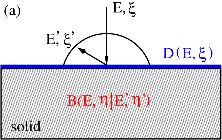
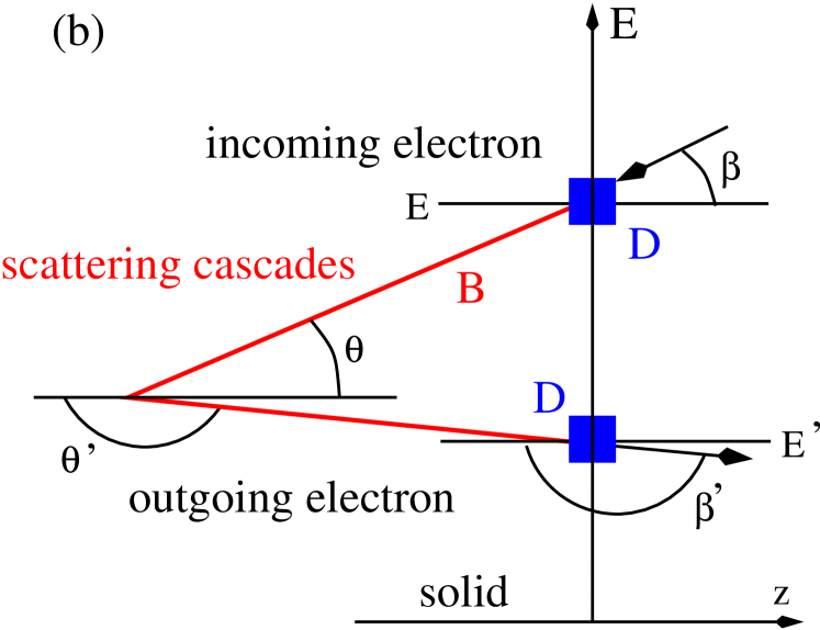
Measuring energy, length, and mass, respectively, in Rydberg energies, Bohr radii, and electron masses, and using the notation introduced in Fig. 1b, the surface scattering kernel relating at the electron energy distribution function of the incoming electrons with the distribution function of the outgoing ones is defined by Cagas et al. (2020)
| (1) |
with and
| (2) |
where is the probability for an electron with energy and direction cosine to be quantum-mechanically reflected by the interface potential and is the part of the kernel accounting for the scattering cascades inside the solid producing a backscattered electron with energy and direction cosine .
The integral relation (1) holds for that part of the incoming electron energy distribution function which describes electrons with energy large enough to overcome the repulsive wall potential. Only this group of electrons hits the material interface and is not reflected by the wall potential. Since we measure energy from the potential just outside the interface, electrons of this group have positive energy. Likewise, electrons leaving the solid require a kinetic energy perpendicular to the interface larger than the electron affinity . Their total energy is thus also positive. Hence, the surface scattering kernel (2) is defined for .
Since the scattering cascade encoded in involves states far away from the extremal points of the conduction band, we do not employ effective electron masses inside the solid as we did before Bronold and Fehske (2015, 2017); Bronold et al. (2018). Instead, we now simply take bare electron masses (also for the holes). This is of course an approximation, but overcoming it requires to account for the full band structure, including nonparabolicities as well as multi-valleys, which is beyond our present scope. It is also not obvious, to what extent band structure details affect the surface scattering kernel and the emission yield quantitatively. It is conceivable that many band structure details are washed out due to the cascade’s multiple scattering. Hence, the conduction band density of states reads and the relation between the internal () and external direction cosines (), to be obtained from the conservation of the lateral momentum and the total energy, becomes from which and its inverse follow. Using, we finally obtain Bronold et al. (2018)
| (3) |
where the Heaviside step function ensures and is the backscattering function to which we turn in the next subsection. Before, however, we note that in terms of the surface scattering kernel, the emission yield is given by
| (4) |
It can be transformed into the expression for given before Bronold and Fehske (2015, 2017); Bronold et al. (2018); Bronold and Fehske (2022)
by changing the integration variables from to
and taking into account that only internal backscattered states with perpendicular kinetic
energy larger than the electron affinity contribute to the emission yield.
II.2 Backscattering function
The central object of our approach is the backscattering function . It describes the (pseudo-)probability for an electron with energy and direction cosine to lead to a backscattered electron with energy and direction cosine . In the previous work Bronold and Fehske (2015, 2017); Bronold et al. (2018); Bronold and Fehske (2022), we considered as a conditional probability, obtained from the function normalized to the totality of all backscattered states, including those, which do not lead to electron escape from the solid. The emission yields we obtained turned out to be in good agreement with experimental data suggesting that the normalization is indeed required. However, in the course of the present investigation we realized that the normalization leads in the limit of particle-conserving scattering processes and vanishing work function (metal) or electron affinity (semiconductor) to an energy and angle independent unitary emission yield. Although in reality not realizable, this cannot be correct. In the following, we therefore abandon the conditional probability construction and identify the backscattering function directly with the function , that is, we set
| (5) |
with obtained, as before Bronold and Fehske (2015, 2017); Bronold et al. (2018); Bronold and Fehske (2022), from the invariant embedding principle Dashen (1964); Glazov and Pázsit (2007); Azzolini et al. (2020).
In its basic form, given by Dashen Dashen (1964) and illustrated in Fig. 2, the principle states that adding an infinitesimally thin layer of the same material on top of a halfspace filled with it does not change the backscattering. Symmetrizing the backscattering function,
| (6) |
the principle leads to the embedding equation,
| (7) |
where the operation is defined by
| (8) |
The kernels, inverse scattering lengths weighted by the direction of propagation, can be obtained from the Golden Rule transition rates for forward and backward () scattering,
| (9) |
whereas
| (10) |
with
| (11) |
the total scattering rate at energy which in fact is independent of . The transition
rates will be specified in the next subsection. The numerical strategy to
solve the embedding equation (7) follows Shimizu and coworkers Shimizu and Mizuta (1966); Shimizu and Aoki (1972)
who used the invariant embedding approach to study the shielding of rays in nuclear
reactors. It is sketched in Appendix A and solves the equation without
approximation except the discretization of the integrals.
II.3 Randium-jellium model
In the previous subsection we described a general scheme for the construction of the surface scattering kernel . To compute numerical values, we have to furnish the approach with a microscopic model for the solid, that is, we have to specify the electronic structure, the interface potential, and the scattering processes inside the semiconductor.
Inspired by the work of Bauer and coworkers Bauer (1970); Dietzel et al. (1982), we employ for that purpose a randium-jellium-type model, with ion cores randomly immersed in an electron liquid. The elastic scattering of electrons on the ion cores is assumed to be incoherent and described by a screened pseudopotential which is also used in electronic band structure calculations Ihm et al. (1978); M. Schlüter, J. R. Chelikowsky, S. G. Louie, and M. L. Cohen (1975); Phillips (1973). Screening is subtle in covalently bound solids. We account for it phenomenologically along the lines of Penn Penn (1962), augmented by ideas of Phillips Phillips (1968) and parameters of Srinivasan Srinivasan (1969). In addition to the scattering on the ion cores, we consider electron-phonon scattering, and as the main energy loss process, impact ionization across the energy gap. The latter causes also electron multiplication and is thus of central importance for secondary electron emission.
| Si | 4 | 5.43 | 4.05 | 1.11 | 0.063 | 11 | 11.7 |
| Ge | 4 | 5.66 | 4.0 | 0.66 | 0.037 | 9.5 | 16.2 |
| Si | -0.992 | 0.791 | -0.352 | -0.018 | 4.8 | 2.33 | 0.0073 |
| Ge | -0.955 | 0.803 | -0.312 | -0.019 | 4.2 | 5.32 | 0.0065 |
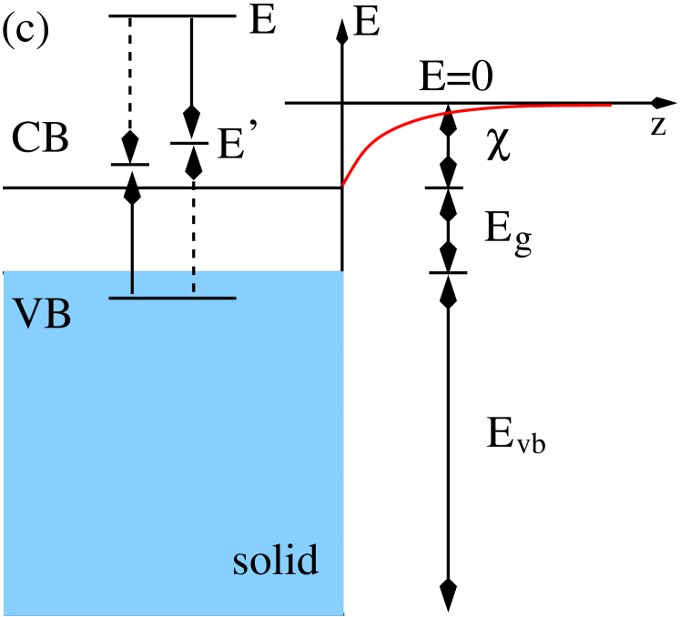
The full band structure of the solid cannot be represented by the randium-jellium model. We hence approximate the electronic structure of the semiconductor by a parabolic conduction and a parabolic valence band, separated by a direct energy gap , and both with effective mass equal to the bare electron mass. Taking then an image-step MacColl (1939) with depth as an interface potential, as indicated in Fig. 1c, the probability for an electron to be quantum-mechanically reflected from the interface region reads Rasek et al. (2022)
| (12) |
with , , and
| (13) |
where is a Whittaker function, its derivative with respect to its argument,
| (14) | ||||
| (15) |
is the complex conjugate of , and is the dielectric constant of the solid. As in the work for metals Bronold and Fehske (2022), energy gaps in the reflection probability could be included. But the experimental data for the emission yield of silicon and germanium Fowler and Farnsworth (1958); Bronshtein and Fraiman (1969), the materials we use as an illustration of our approach, do not indicate that this is required.
We are now turning to the scattering processes inside the solid. Measured from the conduction band minimum, electron emission and reflection take place at energies much larger than phonon energies, even the energy of the longitudinal optical phonon . It is thus appropriate to describe electron-phonon scattering quasi-elastically and to combine it with electron-ion-core scattering to a single elastic scattering process. Since the latter should be absent at low energies, close to the band minimum, we adopt an idea of Kieft and Bosch Kieft and Bosch (2008) and switch between the two elastic scattering processes. Instead of a smooth crossover we implement however a hard energy threshold , above which electrons scatter on the ion cores, whereas below it electrons scatter with phonons. The threshold is the energy, where the electron’s de Broglie wave length measured from the bottom of the conduction band is equal to the lattice spacing. Hence, with the lattice constant and the electron affinity. Albeit ad-hoc, it seems plausible to assume that electrons with small wave length do not notice the lattice periodicity, especially when they propagate in arbitrary directions. Indeed, at energies above 100 eV neglecting the periodicity of the lattice potential seems to be generally accepted (but see the recent discussion by Werner Werner (2023)). Systematic work, based on quantum-kinetic equations, which so far has been only done for high energies Dudarev et al. (1993), is however required to ultimately clarify this point.
The starting point for the calculation of the elastic transition rates is the standard Golden Rule expression. Introducing spherical coordinates in momentum space, with the axis pointing along the inward interface normal, states with describe electrons moving inwards the solid, whereas states with denote states moving outwards. It is then straightforward to work out the rates for forward and backward scattering and to express them in terms of the variables defined in Fig. 1b: the total energy , the direction cosine , and the azimuth angle , which for a laterally homogeneous interface does however not appear because it is integrated out. As a result, one obtains
| (16) |
with the Heaviside step function,
| (17) |
the rate for electron-(longitudinal optical) phonon scattering, where is the scattering strength and the Bose function, and
| (18) |
the electron-ion-core scattering rate with denoting the integral over the azimuth angle, the atomic density of the solid, and
| (19) |
the Fourier transform of the pseudopotential Ihm et al. (1978); M. Schlüter, J. R. Chelikowsky, S. G. Louie, and M. L. Cohen (1975); Phillips (1973) of an ion with valence , phenomenologically screened Srinivasan (1969); Phillips (1968); Penn (1962) as explained below. Its normalization leads to the factor in the scattering rate. Finally,
| (20) |
where the function is defined in (52) and and are the lateral kinetic energies of the initial and final state. The material parameters entering the rates are named and listed in Table 1.
For energies above the band gap, impact ionization is possible and becomes the main inelastic scattering process. To derive its rate, we switch to the hole representation for the valence band and start with the standard Golden Rule representation as given, for instance, by Kane Kane (1967). Using spherical coordinates in momentum space with the axis pointing again inwards, identifying scattering between states for forward and backward moving electrons, and employing the total energy , the lateral kinetic energy (instead of the direction cosine ), and the azimuth angle as independent variables, we obtain
| (21) |
with the function derived in Appendix B and and the lateral kinetic energies given above.
As illustrated in Fig 1c, impact ionization leads to two conduction band electrons Kane (1967); Thoma et al. (1991); Bude et al. (1992); Cartier et al. (1993). To implement in our formalism the correct ionization rate, we thus have to avoid double counting by correctly normalizing, respectively, the contribution of impact ionization to the kernels and the total scattering rate . Following the reasoning of Penn and coworkers Penn et al. (1985), as well as Wolff’s Wolff (1954), we find to be multiplied by a factor two if used in (9) for the kernels ,whereas the plain enters (11) for the total scattering rate . Hence, in total, the transition rates to be used in the kernels read , while in the total scattering rate the rates have to be inserted.
In order to complete the model description, the screening of the electric potentials inside the semiconductor has to be specified. Avoiding a selfconsistent calculation of the potentials, we adopt a phenomenological screening model which combines metal- and semiconductor-type screening. Following Phillips Phillips (1968), we split for that purpose the valence charge into an atomic part, localized close to the ion cores, and a bond part, localized in the bonds between neighboring ions. Anticipating a static dielectric constant , denoting by the valence of the atoms constituting the solid, and measuring charge in units of the elementary charge , the bond charge per ion is , while the atomic charge per ion is . Assuming now, the atomic charges to perfectly screen the charge of the ions, each ion core carries effectively only a charge . Since the bond charge is less localized then the atomic charge, it may approximately give rise to metallic screening, described by a Thomas-Fermi screening wave number defined by
| (22) |
where and is the Fermi energy associated with the bond part of the valence charge density.
The screened Coulomb part of the ion’s pseudopotential would thus become with given by (22). We have to correct however for the fact that part of the valence charge is put into metallic screening. This can be done by using Penn’s formula Penn (1962) for the dielectric constant of a semiconductor not for the total valence charge but only for the atomic part. Hence, in the Coulomb part of the pseudopotential is not multiplied by but by with
| (23) |
where , , and is the average optical band gap Penn (1962); Phillips (1968). Put together, we then obtain the screened Coulomb part of the pseudopotential, , as it features in (19).
Since the impact ionization rate contains the Coulomb interaction between two electrons, and not between an electron and an ion core, we screen it by the full valence charge density in a metallic manner (see Appendix B). Although this is also an approximation, in spirit, it is consistent with previous calculations of the impact ionization rate in semiconductors Kane (1967); Thoma et al. (1991); Bude et al. (1992); Cartier et al. (1993).
III Results
Having established a model for the semiconducting interface, from which the transition rates follow, the kernels of the embedding equation are given and we can solve (7) by the numerical strategy explained in Appendix A to obtain–at the end–the surface scattering kernel as well as the emission yield . To demonstrate the feasibility of our approach we consider silicon and germanium. The parameters of the model are given in Table 1 and the temperature of the solid is . We are particularly interested in low electron impact energies. Setting gives a width for the energy windows into which we split in the numerical implementation the whole energy range from to . The discretization steps of the integrals over the direction cosines lead to .
Let us start with numerical data for , the transition rates to be used in (11) for the calculation of the total scattering rate . The rates employed in (9) for the kernels are the same except of the factor two in front of (see discussion in the paragraph after Eq. (21) of the previous section).
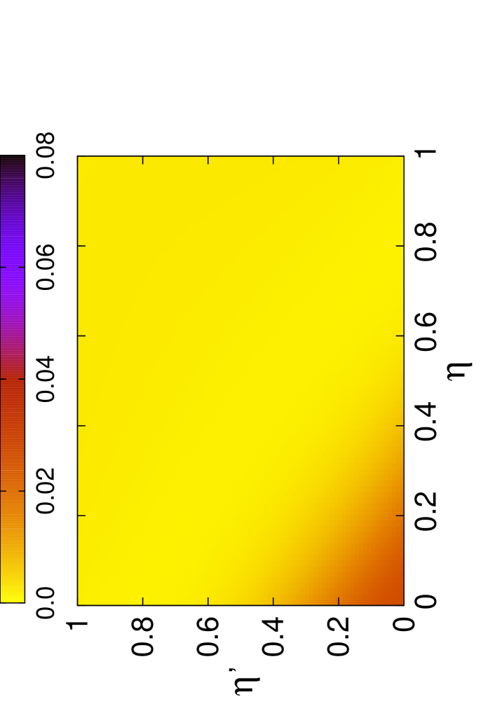
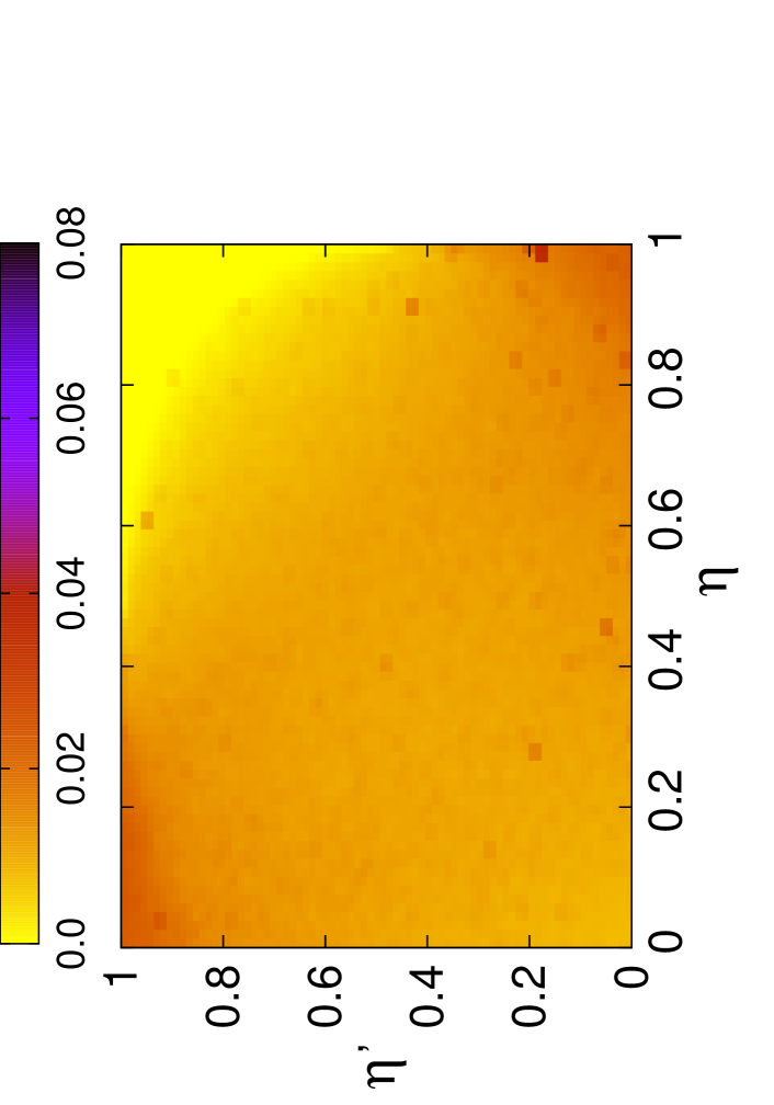
The angle dependence of is depicted in Fig. 3 for the energy doublets , representing elastic scattering, and , standing for inelastic scattering. For the chosen initial () and final state energies (), which are both above the threshold energy , elastic scattering is due to the ion cores. Due to the momentum dependence of the ion’s pseudopotentials forward scattering is thus favored. Hence, , shown in the upper right panel, is peaked around and , plotted on the upper left, is large only for small and , that is, for grazing scattering events. For initial and final state energies below (not shown), where in our model elastic scattering is due to phonons, both rates are isotropic because of the nonpolarity of the phonons, making the scattering strength in (17) momentum independent. This energy range influences however the surface scattering kernel only indirectly via the total scattering rate defined in (11), where the energy integral runs from to . Inelastic scattering in our model is due to impact ionization. From the panels of the second row of Fig. 3 it can be inferred that it does not favor any particular forward or backward direction. It is however again strongest in forward direction and there particularly for and close to unity.
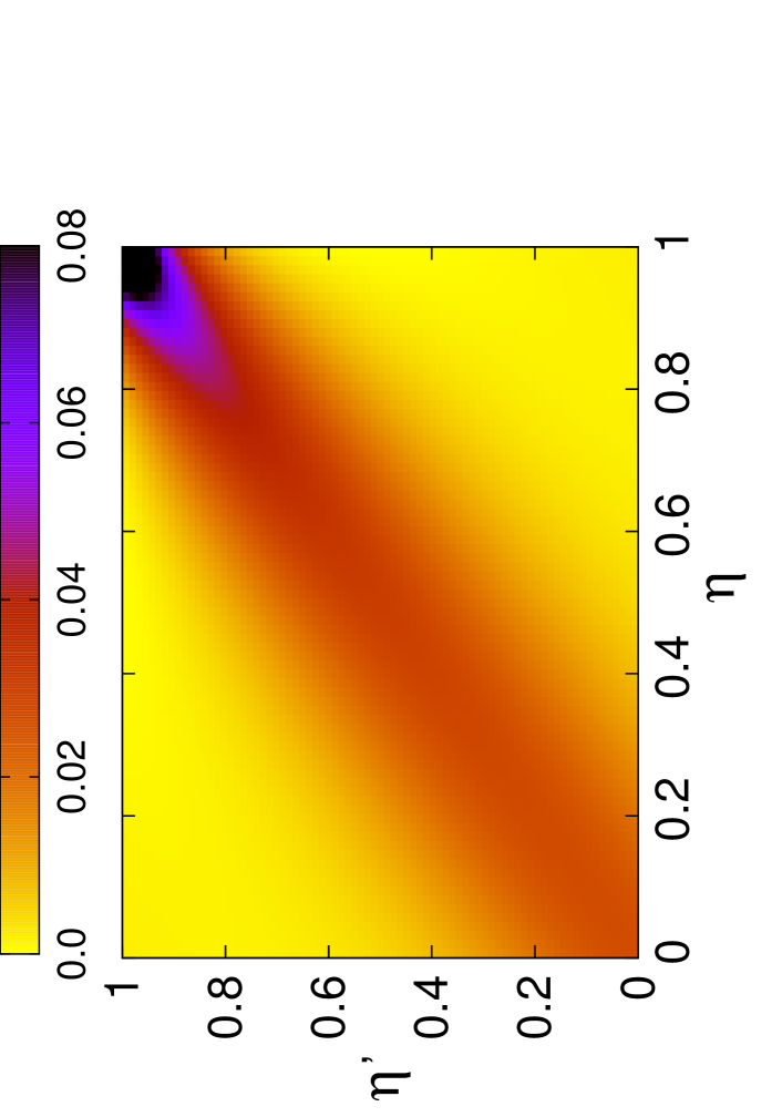
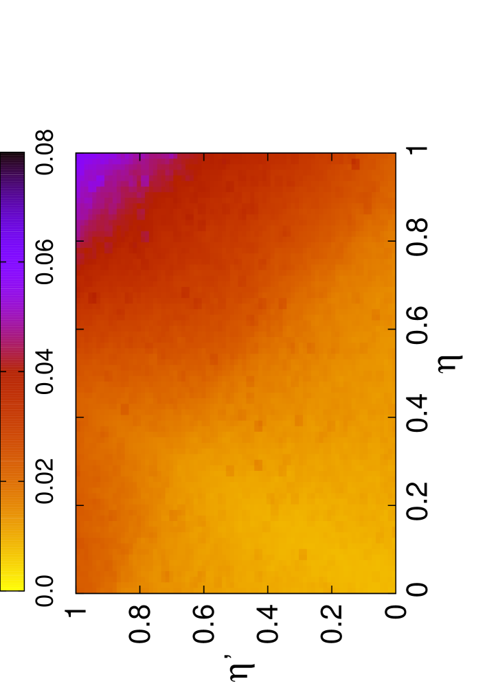
Figure 4 depicts the energy dependence of the transition rates for the direction cosine doublets and . Elastic scattering, below due to phonons and above it due to ion cores, is visible along the energy diagonal, whereas impact ionization leads to the off-diagonal data. Of particular relevance for the surface scattering kernel , and hence also for the secondary emission yield , is the fact that impact ionization favors in backward direction for fixed initial and final direction cosines and large energy transfers. Hence, irrespective of the particular choice of and , the rate is strongest for small . In forward direction small energy transfers also occur, leading to covering larger parts of the plane for a fixed pair and . However, the surface scattering kernel, as well as the emission yield, are determined by the interplay between forward and backward scattering. From the energy dependence of the transition rates we thus expect that most of the backscattered and emitted electrons will have small energy. Hence, they will appear close to the just-outside potential energy indicated by the dashed lines.
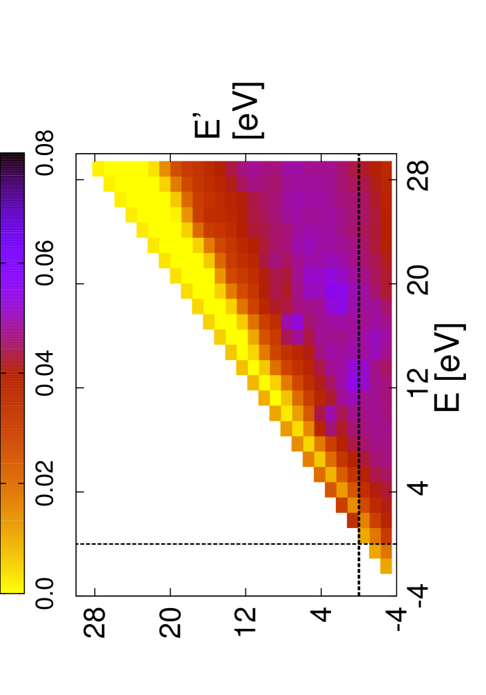
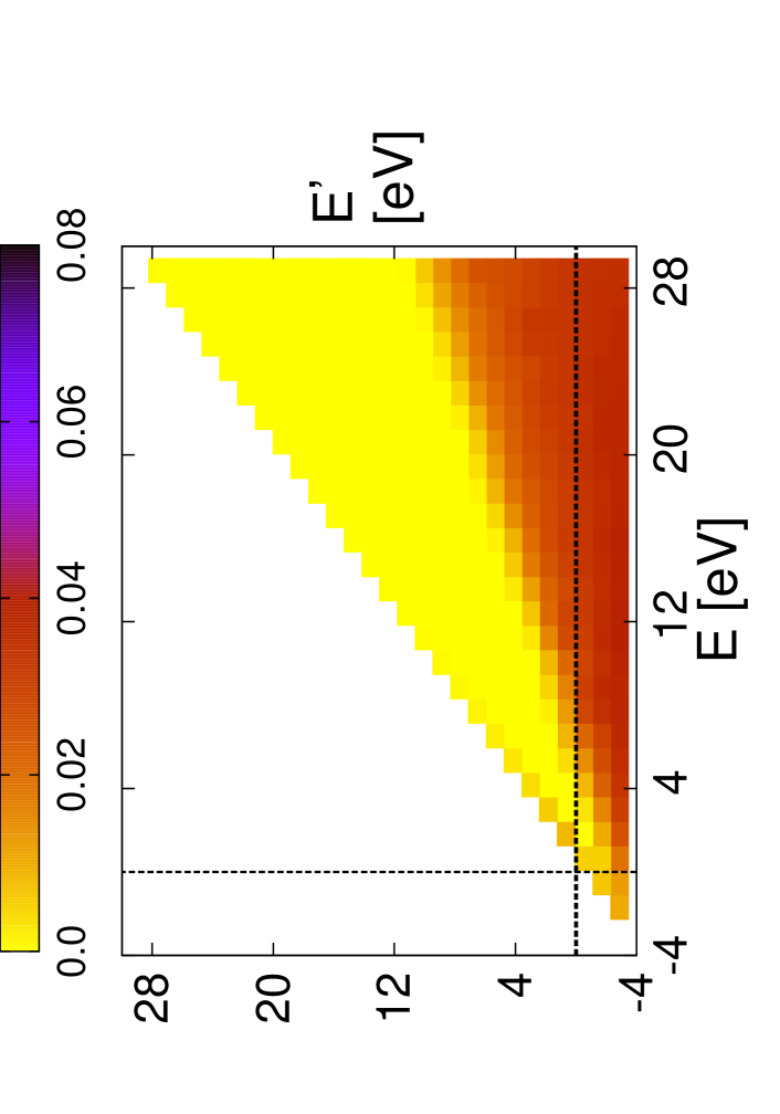
To validate at least partly the calculated transition rates we show in Fig. 5 the total scattering rate for silicon. Without the elastic scattering processes, is the ionization rate and can be compared with the results of others. As discussed by Cartier and coworkers Cartier et al. (1993), there is a substantial spread in the calculated ionization rates. Below the just-outside potential energy, the rates are sensitive to details of the band structure. Since we are interested at energies above it, we do not enter this discussion. To demonstrate that the ionization rate of our model is plausible, we compare it specifically with the rates obtained by Bude and coworkers Bude et al. (1992) and Thoma and coworkers Thoma et al. (1991). Notice, both groups calculate the rate only up to 3-4 eV above the conduction band minimum, that is, below the just-outside potential energy. For impact ionization alone (ii), our data are sufficiently close to the data of the two groups, indicating that the semiconductor model we set up produces reasonable data. Adding the scattering on phonons below and the scattering on ion cores above the threshold energy (ii+ep/eic) modifies the rate. In particular, the sharp on-set of impact ionization at is whipped out and the rate assumes finite values all the way down to the bottom of the conduction band. More important for the surface scattering kernel is however the increase of above the just-outside potential energy which can be also clearly seen. For comparison, we also plot in Fig. 5 the rate for electrons suffering in addition to impact ionization also elastic scattering on phonons (ii+ep) or ions (ii+eic) throughout the whole energy range.
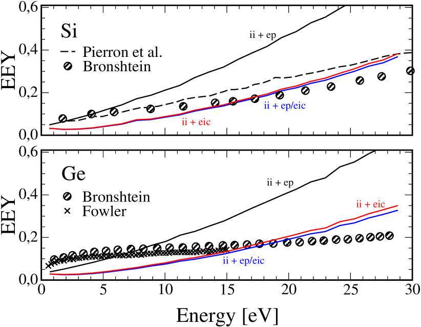
The numerical data for suggest that the model presented in II.3 is sufficiently close to reality to expect plausible emission yields and surface scattering kernels. Let us first look at the emission yields for which experimental data exist. Figure 6 shows calculated emission yields for silicon and germanium together with experimental data from Bronshtein and Fraiman Bronshtein and Fraiman (1969), and Fowler and Farnsworth Fowler and Farnsworth (1958). For silicon the agreement is satisfactory, given the fact that we do not adjust any parameter, working, for instance, with the pseudopotentials also employed in band structure calculations Ihm et al. (1978); M. Schlüter, J. R. Chelikowsky, S. G. Louie, and M. L. Cohen (1975). Our results for silicon are of the same quality as the Monte Carlo results of Pierron and coworkers Pierron et al. (2017), who used however a different model. For germanium the discrepancy between calculated and measured yields is larger. Only the order of magnitude is correct. Since silicon and germanium are similar materials, as can be seen from the material parameters, the failure for germanium is surprising. Further measurements as well as calculations are required to clarify the issue. We also plotted again, for comparison, the yields obtained by letting electron-phonon or electron-ion-core scattering act throughout the whole energy range. Due to the isotropy of electron-phonon scattering in nonpolar semiconductors (see Eq. (17)) the yield obtained by impact ionization and electron-phonon scattering (ii+ep) is largest and substantially off the experimental data suggesting that above the just-outside potential energy a different elastic scattering process should prevail. As discussed in II.3 scattering on the ion cores should become increasingly important for . Indeed, combined with impact ionization scattering on ion cores (ii+eic) produces the best results. Since the threshold energy, where we switch between phonon and ion-core scattering is close to the just-outside level, there is hardly any difference to the data (ii+ep/eic) produced by including this switch. The finding is also in accordance with Monte Carlo simulations of secondary electron emission which unisono incorporate incoherent scattering of electrons on ion cores, as we do, the only difference being in the choice of the scattering potential. Being mostly concerned with energies above they employ screened atomic potentials (see, for instance, Pierron et al. Pierron et al. (2017), Werner Werner (2023), and Dapor’s book Dapor (2020)).
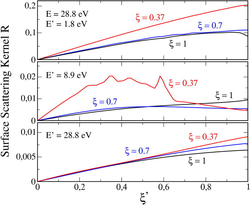
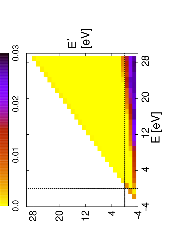
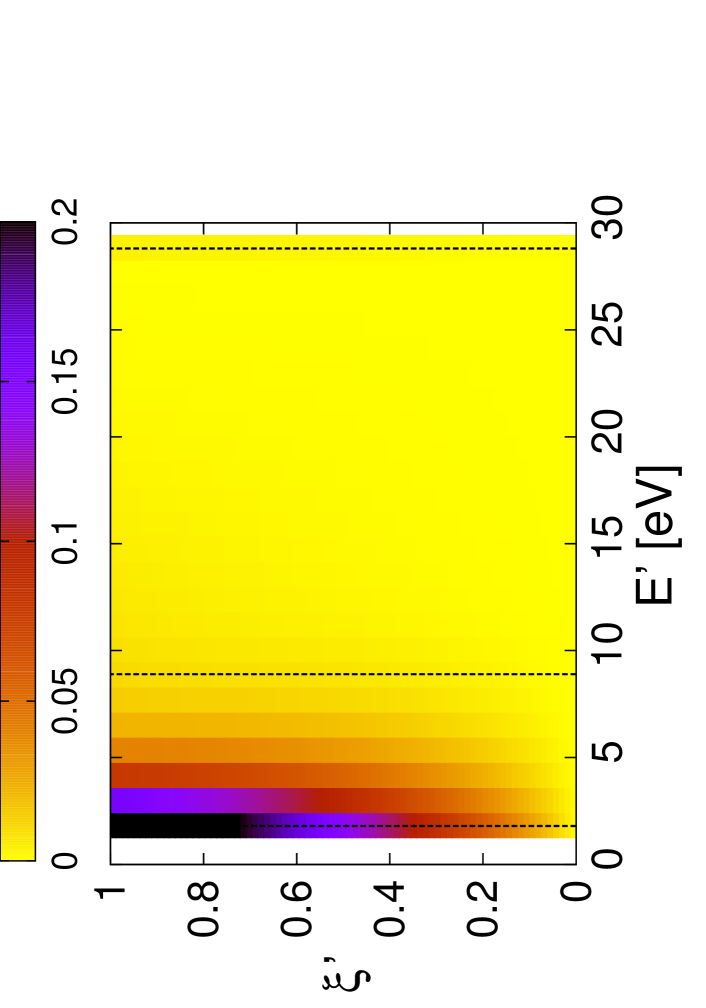
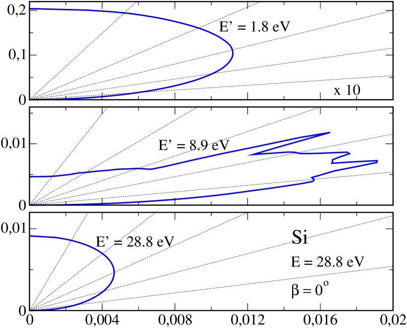
Let us finally take a look at representative data for the surface scattering kernel arising from our model for a silicon-plasma interface. Since for germanium the data are similar, we discuss only silicon. Figure 7 depicts on the left for initial energy and initial direction cosine . As expected from the transition rates’ favoring of large energy transfers, demonstrated in Fig. 4, the surface scattering kernel is largest close to the just-outside potential energy. The polar plots (in ) of the kernel shown on the right of the figure indicate, moreover, that for perpendicular impact the emission occurs essentially isotropically in all spatial directions compatible with the halfspace geometry. Only electrons emitted at intermediate energies, for instance, show a preferred range of emission directions. However, the magnitude of is in this energy range rather small. Hence, the directed emission is rather improbable. The main feature of the data shown on the left of Fig. 7, that the kernel is almost vanishing for , remains intact by reducing . Only for of a few eV the separation breaks down.
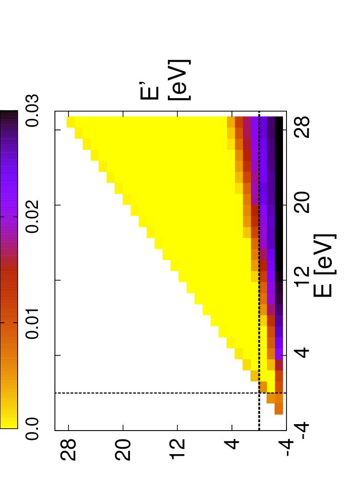
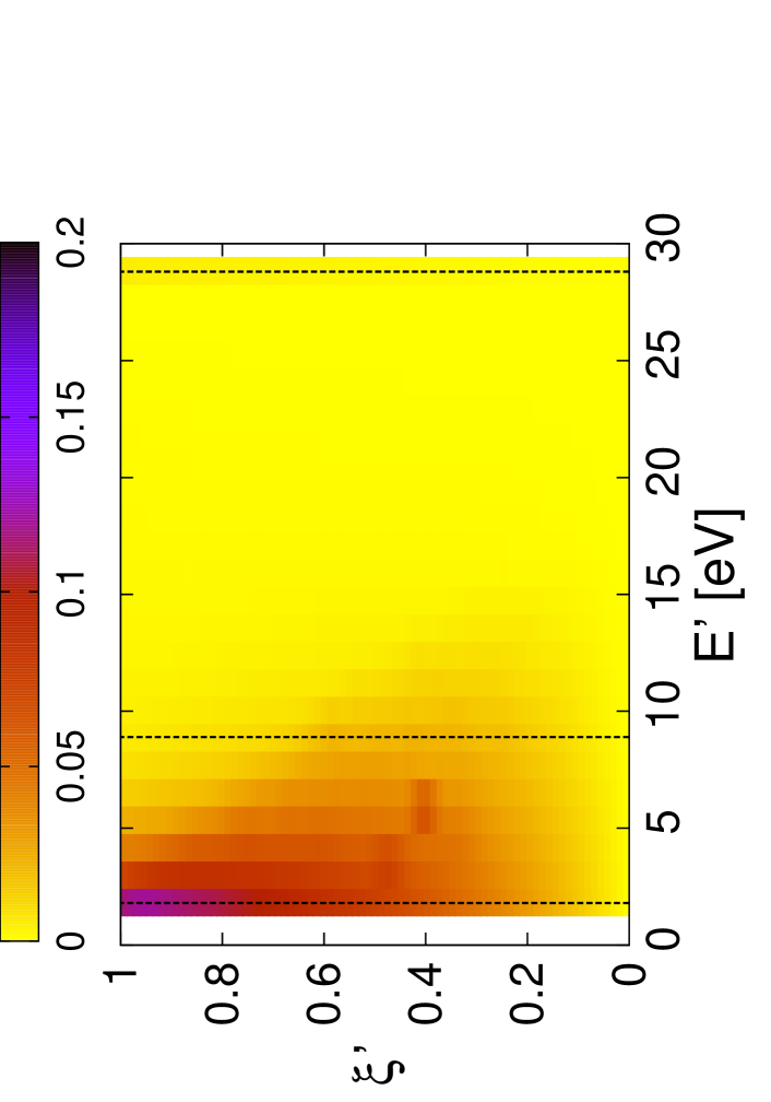
Of interest is also the dependence of the surface scattering kernel on the direction cosine of impact. Figure 8 plots for and , corresponding to . In contrast to the data for , that is, for (perpendicular impact), shown on the left of Fig. 7, the kernel starts now to reach out for faintly to larger . It seems to be also no longer always largest for .
The dependencies on and can be better read off in Fig. 9, where we plot for , three impact direction cosines (corresponding to ), and three emission energies . The scale of the ordinate of the upper panel, showing the data for , is a factor 10 larger than the corresponding one in the middle and lower panels, indicating that irrespective of the direction of impact is in general largest close to the just-outside potential energy. Irrespective of , the magnitude of increases moreover for most values monotonously with . Only at intermediate emission energies and grazing incident, for instance, , develops a very shallow maximum at finite and hence a preferred range of emission directions away from , as already seen in Fig. 8. The feature occurs, however, in an energy range, where is rather small. Most secondary electrons remain hence to be emitted perpendicularly close to the just-outside potential of the surface. Plots for other values of , , and show the same overall features.
To visualize the surface scattering kernel , a function depending on four continuous variables, in its totality is of course impossible. Many more plots could be produced and put on display. They all look rather similar. For the purpose of demonstrating that the surface scattering kernel can be obtained by the invariant embedding approach from a physical model of the plasma-facing solid the plots presented should suffice.
IV Conclusion
We presented a scheme for constructing a boundary condition for the electron energy distribution function of a plasma in contact with a semiconducting solid. Based on the invariant embedding principle for the backscattering function, we derived an expression for the electron surface scattering kernel which takes the electron microphysics inside the solid, responsible for electron backscattering and emission, into account. The kernel connects at the plasma-solid interface the distribution function of the outgoing electrons with the distribution function of the incoming ones. Hence, an electron boundary condition arises which takes material-dependent aspects more faithfully into account as the phenomenological approaches used so far.
As an illustration, we applied the scheme to a silicon and germanium surface, describing the electron’s microphysics inside the solids by a randium-jellium model. Approximating the interface potential by an image-step and taking impact ionization as well as incoherent elastic scattering due to phonons and ion cores into account, we deduced from the surface scattering kernel emission yields in satisfactory agreement with experimental data. For silicon we obtained in fact good agreement, suggesting that the model captures the essential processes leading to electron backscattering and emission sufficiently well.
The main advantage of the embedding approach is that it takes the electron microphysics of the solid into account without tracing the electron distribution function across the plasma-solid interface. It is thus not necessary to run the computation of the surface scattering kernel together with the plasma simulation. The kernel can be computed before hand and stored in a data file. As presented, the approach applies to quasi-stationary situations. It can be, however, generalized to time-dependent situations.
Whereas the transport problem in the form of the embedding equation is completely solved numerically, without linearization and also without an approximate decoupling of direction cosines and energies, the randium-jellium modeling of the electron’s microphysics inside the solid may not be the final answer, not only because of the incomplete agreement with experimental data for germanium, but also due to open conceptual issues. In particular, the scattering on the ion cores needs further studies. We assumed the scattering to be completely incoherent, making our model most appropriate for amorphous surfaces. In crystalline solids there should be however also coherent scattering, leading to distinguished directions for backscattering and emission, as well as band gaps above the just-outside potential energy. The mixed screening model, containing semiconductor and metal like elements, needs also further investigations, taking in particular band structure effects into account.
The randium-jellium model is however a good starting point. Provided pseudopotentials
for the ion cores are available or can be constructed, it can be applied to other
materials as well. Naturally, the scattering and screening processes have to be
adjusted case by case, but in its main features, the model applies to semiconductors,
dielectrics, as well as metals. The plausibility of the kernels, and hence of the
boundary conditions for the electron energy distribution functions, depends
on how well the model captures the microscopic processes responsible for
electron backscattering and emission. In order to determine the quality of the
model, experimental input is critical. Not only measuring the emission yields
and backscattering probabilities of freestanding surfaces is required, but
also operando surface diagnostics of plasma-exposed surfaces, revealing the structural
and chemical state of the surface hit by the electrons of the plasma.
We acknowledge support by the Deutsche Forschungsgemeinschaft through project 495729137.
Appendix A Numerical approach
The numerical method we adopt for solving the embedding equation (7) is due to Shimizu and coworkers Shimizu and Mizuta (1966); Shimizu and Aoki (1972), who used it for studying transport problems in nuclear reactor physics. It utilizes the Volterra-type structure of the energy integrals to transform (7) into a set of matrix equations in the discretized direction cosines and turns out to be surprisingly efficient.
As a first step, the energy space is split into windows of width and for each function a set of functions
| (24) |
is introduced, where denotes the integration over the energy window and is a weight function. In contrast to Shimizu and coworkers, the energy windows we employ have all the same width. Numbering the windows from low to high energy by , and approximating for and inside the windows labelled by and , respectively, the embedding equation reduces to a set of integral equations in the direction cosines. In a straight manner, one obtains for
| (25) |
and for
| (26) |
with
| (27) |
where we introduced a matrix notation in the direction cosines and the operation, which is the operation (8) without the energy integration. In addition we defined the matrices
| (28) | ||||
| (29) | ||||
| (30) | ||||
| (31) |
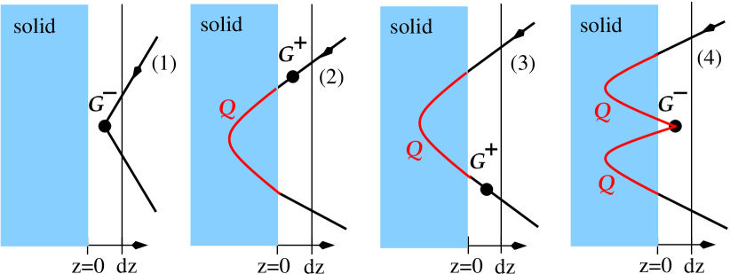
The crux is now to go through the energy space, that is, through the window indices in such a manner that all the matrices appearing in Eqs. (28)–(31) are known from the previous steps of the calculation, enabling thereby an iterative computation of the fixpoints and of, respectively, Eq. (25) and Eq. (26). As shown in Fig. 10, this is possible by first solving (25) for the diagonal elements and then solving (26) for the off-diagonal elements with , where with and .
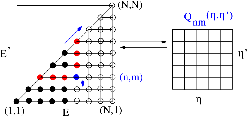
In a second step, the integrals over the direction cosine are discretized. Since we have to switch in the expression for the surface scattering kernel (2) from internal () to external ) direction cosines, we discretized the integrals by a Trapezian rule. Interpolation enables us then to go from to and vice versa.
At the end, the embedding equation (7) is thus turned into a set of matrix equations. To avoid matrix Ricatti and Sylvester equations for and , respectively, it is advantageous to leave on the rhs of Eqs. (25) and (26) only the diagonal matrices . It is then straightforward to iterate for the fixpoint matrices and . For the results discussed in Sect. III we split the energy range with into N=30 energy windows and used M=80 discretization points for the integrals. The function , required for the surface scattering kernel, is finally approximated by
| (32) |
where and belong to the energy windows and , respectively, and the factor involving the density of states arises from the symmetrization (6) which we adopted for a compact representation of the nonlinear term of the embedding equation.
Appendix B Impact ionization rate
Using spherical coordinates for the electron momenta with the axis pointing into the solid and the standard Golden Rule expression Kane (1967); Thoma et al. (1991); Bude et al. (1992); Cartier et al. (1993), the impact ionization rate due to scattering of a conduction band electron with momentum to one with momentum becomes, after one internal momentum integration is carried out, energies and lengths are measured in Rydbergs and Bohr radii, and electron and hole masses are set to the bare electron mass,
| (33) |
with . The squared matrix element for impact ionization reads in the approximation where overlap integrals between single-electron states are set to unity
| (34) |
and the function taking care of the occupancy of the states in the conduction and valence band
| (35) |
with and , where is the Fermi function.
In (35) we anticipated using the total energy , the lateral kinetic energy (or, equivalently, the direction cosine ), and the azimuth angle as independent variables for the conduction band states and defined and , where the minus sign in front of signals that denotes the energy of an hole in the valence band. The electron-electron interaction is given by
| (36) |
with the Thomas-Fermi screening wave number belonging to the total valence charge density and is the Fermi energy associated with it, as discussed at the end of subsection II.3.
To proceed, the integration over is transformed into an integration over , , and , where is the lateral kinetic energy of the valence band hole. Taking care of the Jacobi determinant associated with this variable transformation, measuring azimuth angles with respect to the projection of onto the plane, which is the interface plane, and using the sign of the components of the momenta as labels to distinguish forwardly moving () from backwardly moving electron states, the rate becomes after integrating out with the help of the energy-conserving -function contained in (35),
| (37) |
with
| (38) | ||||
| (39) | ||||
| (40) | ||||
| (41) |
and
| (42) | ||||
| (43) | ||||
| (44) |
where is the Heaviside step function and
| (45) | ||||
| (46) | ||||
| (47) |
The functions and contained in are defined by
| (48) | ||||
| (49) |
where
| (50) | ||||
| (51) | ||||
| (52) |
Due to the independent variables , , and suggested by the interface geometry, the final expression for the impact ionization rate looks a bit messy. It follows however straight from energy and momentum conservation. The three remaining integrals in (37) have to be done numerically. For the data presented in Sect. III we employed the Vegas Monte Carlo integrator of the Numerical Recipes Press et al. (1996).
References
- Weltmann et al. (2019) K.-D. Weltmann, J. F. Kolb, M. Holub, D. Uhrlandt, M. S̆imek, K. Ostrikov, S. Hamaguchi, U. Cvelbar, M. C̆ernák, B. Locke, et al., Plasma Process. Polym. 16, e1800118 (2019).
- R. Michaud and V. Felix and A. Stolz and O. Aubry and P. Lefaucheux and S. Dzikowski and V. Schulz-von der Gathen and L. J. Overzet and R. Dussart (2018) R. Michaud and V. Felix and A. Stolz and O. Aubry and P. Lefaucheux and S. Dzikowski and V. Schulz-von der Gathen and L. J. Overzet and R. Dussart, Plasma Sources Sci. Technol. 27, 025005 (2018).
- Eden et al. (2013) J. G. Eden, S.-J. Park, J. H. Cho, M. H. Kim, T. J. Houlahan, B. Li, E. S. Kim, T. L. Kim, S. K. Lee, K. S. Kim, et al., IEEE Trans. Plasma Sci. 41, 661 (2013).
- Dussart et al. (2010) R. Dussart, L. J. Overzet, P. Lefaucheux, T. Dufour, M. Kulsreshath, M. A. Mandra, T. Tillocher, O. Aubry, S. Dozias, P. Ranson, et al., Eur. Phys. J. D 60, 601 (2010).
- Campanell (2020) M. D. Campanell, Phys. Plasmas 27, 042511 (2020).
- Tolias et al. (2020) P. Tolias, M. Komm, S. Ratynskaia, and A. Podolnik, Nucl. Mat. and Energy 25, 100818 (2020).
- Vignitchouk et al. (2018) L. Vignitchouk, G. L. Delzanno, P. Tolias, and S. Ratynskaia, Phys. Plasmas 25, 063702 (2018).
- Tolias (2014) P. Tolias, Plasma Phys. Control. Fusion 56, 045003 (2014).
- Raitses et al. (2005) Y. Raitses, D. Staack, M. Keidar, and N. J. Fisch, Phys. Plasma 12, 057104 (2005).
- Dunaevsky et al. (2003) A. Dunaevsky, Y. Raitses, and N. J. Fisch, Phys. Plasma 10, 2574 (2003).
- M. M. R. Williams (1971) M. M. R. Williams, Mathematical methods in particle transport theory (Butterworth, London, 1971).
- Kogan (1969) M. N. Kogan, Rarefied gas dynamics (Plenum Press, New York, 1969).
- Al’pert et al. (1965) Y. L. Al’pert, A. V. Gurevich, and L. P. Pitaevskii, Space physics with artificial satellites (Consultants Bureau, New York, 1965).
- Cercignani (1995) C. Cercignani, Revista del Nuovo Cimento 18, 1 (1995).
- Kuscer (1971) I. Kuscer, Surf. Sci. 25, 225 (1971).
- Cercignani and Lampis (1971) C. Cercignani and M. Lampis, Transport Theory Stat. Phys. 1, 101 (1971).
- Becker et al. (2010) M. M. Becker, G. K. Grubert, and D. Loffhagen, Eur. Phys. J. Appl. Phys. 51, 11001 (2010). B
- Loffhagen et al. (2002) D. Loffhagen, F. Sigeneger, and R. Winkler, J. Phys. D: Appl. Phys. 35, 1768 (2002).
- Alves et al. (1997) L. L. Alves, G. Gousset, and C. M. Ferreira, Phys. Rev. E 55, 890 (1997).
- Schulze et al. (2022) C. Schulze, Z. Donkó, and J. Benedikt, Plasma Sources Sci. Technol. 31, 105017 (2022).
- Daksha et al. (2016) M. Daksha, B. Berger, E. Schuengel, I. Korolov, A. Derzsi, M. Koepke, Z. Donkó, and J. Schulze, J. Phys. D: Appl. Phys. 49, 234001 (2016).
- Demidov et al. (2015) V. I. Demidov, S. F. Adams, I. D. Kaganovich, M. E. Koepke, and I. P. Kurlyandskaya, Phys. Plasma 22, 104501 (2015).
- Daksha et al. (2019) M. Daksha, A. Derzsi, Z. Mujahid, D. Schulenberg, B. Berger, Z. Donkó, and J. Schulze, Plasma Sources Sci. Technol. 28, 034002 (2019).
- Dashen (1964) R. Dashen, Phys. Rev. 134, A1025 (1964).
- Glazov and Pázsit (2007) L. G. Glazov and I. Pázsit, Nucl. Instr. and Meth. B 256, 638 (2007).
- Azzolini et al. (2020) M. Azzolini, O. Y. Ridzel, P. S. Kaplya, V. Afanas’ev, N. M. Pugno, S. Taioli, and M. Dapor, Comp. Mat. Sci. 173, 109420 (2020).
- Bronold and Fehske (2015) F. X. Bronold and H. Fehske, Phys. Rev. Lett. 115, 225001 (2015).
- Bronold and Fehske (2022) F. X. Bronold and H. Fehske, J. Appl. Phys. 131, 113303 (2022).
- Cagas et al. (2020) P. Cagas, A. Hakim, and B. Srinivasan, J. Comput. Phys. 406, 109215 (2020).
- Shimizu and Mizuta (1966) A. Shimizu and H. Mizuta, J. Nucl. Sci. Technol. 3, 57 (1966).
- Shimizu and Aoki (1972) A. Shimizu and K. Aoki, Application of invariant embedding to reactor physics (Academic Press, New York, 1972).
- Bronold and Fehske (2017) F. X. Bronold and H. Fehske, Plasma Phys. Control. Fusion 59, 014011 (2017).
- Bronold et al. (2018) F. X. Bronold, F. Fehske, M. Pamperin, and E. Thiessen, Eur. Phys. J. D 72, 88 (2018).
- Kane (1967) E. O. Kane, Phys. Rev. 159, 624 (1967).
- Thoma et al. (1991) R. Thoma, H. J. Pfeifer, W. L. Engl, W. Quade, R. Brunetti, and C. Jacoboni, J. Appl. Phys. 69, 2300 (1991).
- Bude et al. (1992) J. Bude, K. Hess, and G. J. Iafrate, Phys. Rev. B 45, 10958 (1992).
- Cartier et al. (1993) E. Cartier, M. V. Fischetti, E. A. Eklund, and F. R. McFeely, Appl. Phys. Lett. 62, 3339 (1993).
- Bauer (1970) E. Bauer, J. Vac. Sci. Technol. 7, 3 (1970).
- Dietzel et al. (1982) W. Dietzel, G. Meister, and E. Bauer, Z. Phys. B 47, 189 (1982).
- Srinivasan (1969) G. Srinivasan, Phys. Rev. 178, 1244 (1969).
- Phillips (1968) J. C. Phillips, Phys. Rev. 166, 832 (1968).
- Penn (1962) D. R. Penn, Phys. Rev. 128, 2093 (1962).
- Ihm et al. (1978) J. Ihm, S. G. Louie, and M. L. Cohen, Phys. Rev. B 18, 4172 (1978).
- M. Schlüter, J. R. Chelikowsky, S. G. Louie, and M. L. Cohen (1975) M. Schlüter, J. R. Chelikowsky, S. G. Louie, and M. L. Cohen, Phys. Rev. B 12, 4200 (1975).
- Phillips (1973) J. C. Phillips, Bonds and bands in semiconductors (Academic Press, New York, 1973).
- MacColl (1939) L. A. MacColl, Phys. Rev. 56, 699 (1939).
- Fowler and Farnsworth (1958) H. A. Fowler and H. E. Farnsworth, Phys. Rev. 111, 103 (1958).
- Bronshtein and Fraiman (1969) I. M. Bronshtein and B. C. Fraiman, Secondary electron emission (Nauka, Moscow, 1969).
- Pierron et al. (2017) J. Pierron, C. Inguimbert, M. Belhaj, T. Gineste, J. Puech, and M. Raine, J. Appl. Phys. 121, 215107 (2017).
- Jacoboni and Reggiani (1983) C. Jacoboni and L. Reggiani, Rev. Mod. Phys. 55, 645 (1983).
- Rasek et al. (2022) K. Rasek, F. X. Bronold, and H. Fehske, Phys. Rev. E 105, 045202 (2022). B
- Kieft and Bosch (2008) E. Kieft and E. Bosch, J. Phys. D: Appl. Phys. 41, 215310 (2008).
- Werner (2023) W. W. Werner, Front. Mater.10:1202456 (2023).
- Dudarev et al. (1993) S. L. Dudarev, L.-M. Peng, and M. J. Whelan, Phys. Rev. B 48, 13408 (1993).
- Penn et al. (1985) D. R. Penn, S. P. Apell, and S. M. Girvin, Phys. Rev. B 32, 7753 (1985).
- Wolff (1954) P. A. Wolff, Phys. Rev. 95, 56 (1954).
- Dapor (2020) M. Dapor, Transport of energetic electrons in solids (Springer Nature, Cham, Switzerland, 2020).
- Press et al. (1996) W. H. Press, S. A. Teukolsky, W. T. Vetterling, and B. P. Flannery, Numerical recipes (Cambridge University Press, Cambridge, 1996).