Tunable magnetic domains in ferrimagnetic MnSb2Te4
Abstract
Highly tunable properties make Mn(Bi,Sb)2Te4 a rich playground for exploring the interplay between band topology and magnetism: On one end, MnBi2Te4 is an antiferromagnetic topological insulator, while the magnetic structure of MnSb2Te4 (MST) can be tuned between antiferromagnetic and ferrimagnetic. Motivated to control electronic properties through real-space magnetic textures, we use magnetic force microscopy (MFM) to image the domains of ferrimagnetic MST. We find that magnetic field tunes between stripe and bubble domain morphologies, raising the possibility of topological spin textures. Moreover, we combine in situ transport with domain manipulation and imaging to both write MST device properties and directly measure the scaling of the Hall response with domain area. This work demonstrates measurement of the local anomalous Hall response using MFM, and opens the door to reconfigurable domain-based devices in the M(B,S)T family.
The recent discovery of MnBi2Te4 (MBT) [1, 2, 3, 4, 5] was a breakthrough to realize the quantum anomalous Hall effect in a stoichiometric crystal, avoiding the need for disorder-inducing magnetic dopants [6, 7, 8, 9]. In addition, crystals are exfoliatable down to few layer thicknesses enabling integration into Van der Waals heterostructures with well developed fabrication techniques [1, 10, 11, 12]. This discovery was rapidly followed by work extending MBT into a family of materials with highly tunable properties via crystallographic and chemical paradigms [13, 14, 15, 16, 17, 18, 19, 4, 20, 21, 5]. Substituting Sb for Bi changes the doping from n-type to p-type [16, 22]. But surprisingly, within MST, the magnetic order can also be tuned (via the concentration of magnetic defects) from A-type antiferromagnetic seen in MBT, where planes of Mn moments are aligned ferromagnetically (antiferromagnetically) within the plane (between planes), to ferrimagnetic with net out of plane magnetization [19, 23, 21, 24, 25]. The ability to tune the effective inter-plane coupling from antiferromagnetic to ferromagnetic strongly suggests the presence of magnetic frustration in M(B,S)T, raising the possibility of stabilizing other interesting magnetic orders [26, 27].
The ability to tune magnetic order in the M(B,S)T family opens more conventional applications of magnetic materials, where intense efforts have gone into developing materials structures with interdependent magnetic and electronic properties for control of charge and spin transport (e.g. magnetic data storage and spintronics). Growing evidence suggests that the low energy bands of MST are sensitive to the details of magnetic order [19, 3, 28, 29, 24, 30], but we do not yet have a detailed understanding of the correlation between electronic properties and real-space magnetic textures in MST. So far, the use of magnetism to control electronic properties in magnetic topological materials has been explored primarily in terms of topological phase transitions (e.g. [28, 10, 31, 12]) and manipulating chiral edge modes of the quantum anomalous Hall effect [32, 33, 11]. Edge mode manipulation has been demonstrated via magnetic domains in Cr-doped (Bi,Sb)2Te3 [32, 33] and via layer-dependent magnetization in antiferromagnetic MBT [11], but to the best of our knowledge, the ability to write arbitrary-shaped domains in ferrimagnetic M(B,S)T compounds has yet to be investigated. In this work, we therefore set out to investigate what magnetic textures can be realized in MST, and the prospects for manipulating the local magnetization to create configurable devices. Specifically, we use the domain imaging and writing capabilities of magnetic force microscopy (MFM) combined with in situ transport to directly measure the device response to local changes in magnetization.
Our interdependent transport and magnetic measurements were performed on an exfoliated flake of ferrimagnetic MST (Figure 1a) with average thickness 84 nm and nm variations (Supporting Information SII). Four gold contacts were used to measure longitudinal and Hall resistance. Immediately after device fabrication, showed a peak at 27 K on cooling, consistent with typical Curie temperatures seen in MST. At 2K, the hysteretic loop in and peaks in as a function of magnetic field showed a coercive field near 10 mT (Supporting Information SIV). Refer to Supporting Information SI for additional details of sample fabrication and characterization.
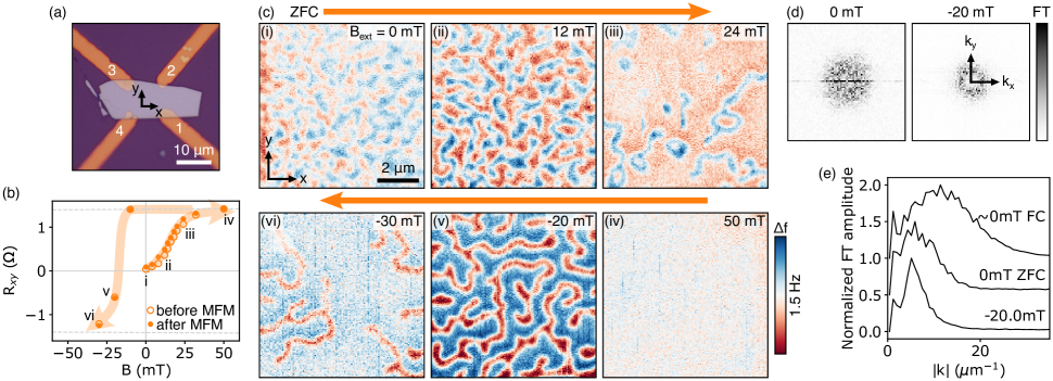
To characterize the magnetic domains in MST, we performed MFM in a cryogenic atomic force microscope (AFM) with variable magnetic field normal to the sample surface. Figure 1c-i shows a MFM image of the zero-field cooled (ZFC) sample at 5 K. Because the coercive field of MST is so low, we quenched the superconducting magnet prior to cooling the sample to ensure a true ZFC with no trapped flux. The MFM image is a measurement of , the resonance frequency shift of the AFM cantilever due to the interaction of the sample’s stray fields with the cantilever’s magnetic tip, so we expect images to primarily detect the domain structure of the ferromagnetically aligned components of MST’s ferrimagnetic ordering [34, 35]. Correspondingly, the ZFC image shows disordered maze-like stripe domains (Figure 1) consistent with ferromagnetic ordering in the out of plane direction, similar to domain images from Ge et al [25]. Applying magnetic field normal to the sample surface polarizes the sample (c-i to iv), increasing the area of the domains aligned with the field until at 50 mT, only a single domain remains, giving a uniform MFM signal. In situ transport measurements show an associated increase in from 0.04 to 1.42 . Over this range of , the contribution to from the linear Hall effect is negligible, so the change in is primarily due to the anomalous Hall Effect (AHE) [36] (Supporting Information SVII).
Reversing the magnetic field (Figure 1c-iv to vi), we observe the reformation of stripe domains at -20 mT as drops and changes sign, indicating the reversal of the magnetization. These field-reversed domains are significantly less disordered than the ZFC domains. To quantify the difference, we examine the Fourier Transforms (FT) of the ZFC and -20 mT images, shown in Figure 1d. Both exhibit a ring shape, or a peak in the angular-averaged FT (Figure 1e), indicating the domains have a characteristic length scale, as expected from the energetics of domain formation [37, 38, 39]. The peak occurs at wavevector 6.3 with standard deviation 4.8 for the ZFC domains and 5.7 with 2.1 for the -20 mT domains. The broader peak associated with the ZFC domains indicates that during cooling the domains form features with a wider range of length scales compared to during magnetization reversal at low temperature.
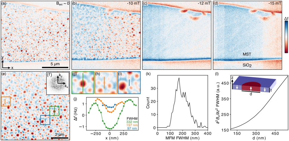
To further explore how an external field can tune the domain morphology, we cooled the MST device from 35 K below under up to 15 mT (Figure 2). With larger than 10 mT, a single domain forms across the entire MST flake. However, when we nominally zero the magnet’s current such that a small exists only from trapped flux, we see circular features in the MFM, indicating the formation of bubble rather than stripe domains. MST is thus remarkably sensitive to small magnetic fields. At intermediate (10 mT), the domains formed are not uniform in size and shape, and it is not clear if they are intrinsically bubbles or stripes. We now focus on , where bubbles are clearly observed.
The bubble domains are highly disordered (Figure 2e). The nearly isotropic Fourier transform (f) shows no evidence for lattice organization, and the distribution of wavevectors centered at 11.3 with 7 is extremely broad. Correspondingly, the circular MFM features range in size from below 100 nm to above 300 nm, as shown by the distribution of full width at half maxima (FWHM, Figure 2k). The size of the features seen in MFM cannot directly be interpreted as the size of the domains in the MST. Approximating the tip as a point dipole with small oscillation amplitude, the MFM image is proportional to arising from the sample’s stray field [34, 35]. To help interpret the MFM features, we model the stray field for a single cylindrical bubble domain at a representative height . As the domain diameter decreases below , the spatial peak in decreases in intensity ( Supporting Information SV) and the FWHM saturates at a lower limit near 150 nm (Figure 2l). The FWHM does not decrease linearly in the domain diameter for small bubbles. Returning to the MFM data, we therefore expect small bubbles may not be detectable due to weak intensity, and for slightly larger bubbles, the apparent size in MFM may saturate at a lower limit larger than the domain diameter. The MFM data, however shows bubbles with FWHM below the expected 150 nm cuttoff, likely because the width of the low intensity bubbles can be dominated by the positions of the neighboring bubbles. Under repeat cooling, we find that some but not all bubbles form in the same location (Supporting Information SIX), which along with their disordered organization could indicate significant pinning, either due to crystal inhomogeneity, or extrinsic factors such as strain. The observation of bubble domains under field cooling, but not when sweeping at low temperature suggests that the bubble and stripe morphologies are separated by a significant energy barrier, likely associated with nucleating a domain wall.
The domain wall structure (i.e. Bloch or Néel) can produce topologically non-trivial chiral spin textures on bubble domains [40], and topological bubble and skyrmion phases have been reported in other (Bi,Sb)2Te3-based materials [41, 42]. While our detection of bubble domains opens the possibility of stabilizing topological spin textures in M(B,S)T, our MFM measurements do not allow us to draw a conclusion about the topology of the bubbles. We observed no evidence of a topological Hall effect (THE) – a deflection of carriers due to the real space Berry curvature of topological spin textures – in the hysteresis loops when sweeping to flip the sample magnetization at low temperature. However, unlike many skyrmion materials that display a THE as the skyrmion phase is formed over a finite range of at constant temperature, the MFM data in Figure 1 does not show the bubble morphology when sweeping at low temperature. Further work is therefore required to determine if the bubble domains formed on field cooling are topological or trivial.
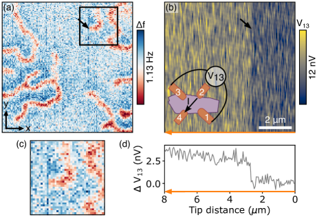
We have seen how the domain morphology can be controlled with ; now we investigate the possibility of using the stray field from the magnetic MFM tip, , to locally manipulate the domains in MST. To reduce the influence of on the sample, the domain imaging discussed so far was done with the tip lifted high (roughly 200-230 nm) above the MST surface. However, when is near the coercive field, small changes in the magnetic field can have a large influence on the sample magnetization, and even 200 nm from the tip, could be on the order of 10 mT [43], comparable to the coercive field. Correspondingly, small changes in and during MFM imaging (Figure 1b, Supporting Information SIV) demonstrate that the tip mildly influenced the sample magnetization. Moreover, tip-induced domain flips are seen in some images as a domain that abruptly disappears partway through imaging. To quantify the tip’s influence, we applied an AC current between contacts 2 and 4, and measured the induced transverse voltage across contacts 1 and 3 during MFM imaging. The MFM image in Figure 3a shows a domain flip, and the simultaneously acquired image (b,d) shows an abrupt change by more than 2 nV at the same location, demonstrating a measurable impact of the domain flip on the device transport. Interestingly the tip-induced domain flips are not always in the sense of aligning the domain with the tip, suggesting that the spatial gradient or time-dependence of may be equally important or more important for overcoming energy barriers compared to the local Zeeman energy term.
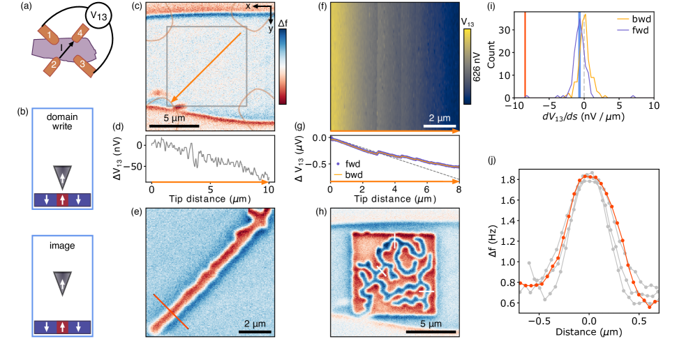
We can harness the tip’s influence to controllably write domains by bringing the tip close to the MST surface, increasing . For this purpose, we first used to prepare the sample with magnetization anti-aligned to the tip (Figure 4c). After zeroing , we then brought the tip into amplitude-controlled feedback on the MST surface ( on the order of 50 mT [43]), and moved the tip across the surface to write a domain aligned with the tip. In Figure 4, we show both linear (e) and square (h) areas written with the MFM tip, demonstrating that both narrow 1D-like and 2D domains can be written. During the write process, the square area formed a mixed domain state, suggesting that because the mixed domain state is energetically favored at , there is a maximum single-domain area of roughly several m2 (Supporting Information SXI) that can be written. Decreasing temperature to increase the importance of the domain wall nucleation energy may increase that area.
By inverting the magnetization of a small area locally with our MFM tip, we can directly probe that area’s impact on the AHE. During domain writing we therefore recorded as a proxy for (Supporting Information SVIII). While writing the line domain, decreased linearly (Figure 4d), matching the area-scaling that one would expect for AHE contributions [36] that scale linearly with the sample average magnetization. recorded while writing the square domain is also consistent with area scaling. Here, forms two 2D images for forward (Figure 4f) and backward scans–to write the domain, the tip moved up and down along each scan line before advancing one pixel at a time left to right. Typically, has a finite slope on the forward pass (the blue histogram in i is peaked at 0.6 nVm), confirming that the tip is writing a magnetization, but not on the backward pass (orange histogram, peaked at zero). Considering that typically each scan line advances the domain wall by one pixel width (53 nm), we can quantify the local AHE: 11 nV/. This value is quantitatively consistent with both: (1) the linear seen when writing the line domain, and (2) the ratio of the change in from before to after the write step to the domain area imaged via MFM (Supporting Information SXI). Moreover, the entire evolution of during the square write can be understood in detail as a linear decrease (gray dashed line in g) from writing the red domain plus deviations from forming the inner blue domain, in abrupt steps initially but then more smoothly near the end of the write.
We have therefore demonstrated a direct measurement of the scaling of the anomalous Hall effect with domain area. The technique can also in principle measure deviations from this area scaling to probe local properties of inhomogenous devices (spatially varying magnetization or Berry curvature). Within homogenous materials, the area-scaling contributions and deviations represent bulk and boundary contributions, meaning that this technique can be used to probe topological effects such as dissipationless chiral edge conduction in a Chern insulator or the topological Hall effect from chiral spin textures at domain walls.
This work opens the door to making programmable magnetic devices within ferrimagnetic compounds in the M(B,S)T family. M(B,S)T could be a platform for writable chiral currents (e.g. [32, 33, 11]) either in a magnetic Weyl semimetal or Chern insulating state (multiple potential band topologies have been predicted in MST [16, 3, 19, 30, 29, 22]). The ability to tune magnetic domains in a compound that retains magnetic order when exfoliated to the few layer limit [16, 1, 31, 44] raises the possibility of using M(B,S)T to introduce programmable magnetic landscapes (e.g. supperlattices or boundaries made of magnetic gradients) on length scales of 100s of nanometers to micrometers into van der Waals heterostructures. Generically, the tip writing process allows us to locally move between different metastable magnetic configurations that are separated by energetic barriers. So beyond writing individual domains of uniform magnetization explicitly, the tip influence could be combined with external fields and temperature to stabilize and write areas of non-uniform spin textures (just as the mixed domain state formed in our square area was not uniform) in order to create functional devices based on boundaries between magnetic phases.
Supporting Information
Additional experimental details, characterization of the sample topography, images of stripe domains, electrical transport measurements, analysis and modelling of domain length scales, analysis of the repeatability of bubble domain locations, and analysis of the scaling of the AHE with domain area (PDF)
Acknowledgements.
We thank Zachariah Addison and Nishchhal Verma for helpful discussions. This work was supported by the Air Force Office of Scientific Research via grant FA9550-21-1-0378 (T.A.W., A.N.P.) and by NSF grants DMR-2210186 (D.N.B) and HRD-2112550 (L.K.-E.). Research on topological properties of moiré superlattices is supported as part of Programmable Quantum Materials, an Energy Frontier Research Center funded by the U.S. Department of Energy (DOE), Office of Science, Basic Energy Sciences (BES), under award DE-SC0019443. Sample synthesis is supported by the the NSF MRSEC program through Columbia University in the Center for Precision-Assembled Quantum Materials under award number DMR-2011738.References
- Deng et al. [2020] Y. Deng, Y. Yu, M. Z. Shi, Z. Guo, Z. Xu, J. Wang, X. H. Chen, and Y. Zhang, Quantum anomalous Hall effect in intrinsic magnetic topological insulator MnBi2Te4, Science 367, 895 (2020).
- Otrokov et al. [2019] M. M. Otrokov, I. I. Klimovskikh, H. Bentmann, D. Estyunin, A. Zeugner, Z. S. Aliev, S. Gaß, A. U. B. Wolter, A. V. Koroleva, A. M. Shikin, M. Blanco-Rey, M. Hoffmann, I. P. Rusinov, A. Y. Vyazovskaya, S. V. Eremeev, Y. M. Koroteev, V. M. Kuznetsov, F. Freyse, J. Sánchez-Barriga, I. R. Amiraslanov, M. B. Babanly, N. T. Mamedov, N. A. Abdullayev, V. N. Zverev, A. Alfonsov, V. Kataev, B. Büchner, E. F. Schwier, S. Kumar, A. Kimura, L. Petaccia, G. Di Santo, R. C. Vidal, S. Schatz, K. Kißner, M. Ünzelmann, C. H. Min, S. Moser, T. R. F. Peixoto, F. Reinert, A. Ernst, P. M. Echenique, A. Isaeva, and E. V. Chulkov, Prediction and observation of an antiferromagnetic topological insulator, Nature 576, 416 (2019).
- Zhang et al. [2019] D. Zhang, M. Shi, T. Zhu, D. Xing, H. Zhang, and J. Wang, Topological Axion States in the Magnetic Insulator MnBi2Te4 with the Quantized Magnetoelectric Effect, Phys. Rev. Lett. 122, 206401 (2019).
- Lei et al. [2020] C. Lei, S. Chen, and A. H. MacDonald, Magnetized topological insulator multilayers, Proc. Natl. Acad. Sci. 117, 27224 (2020).
- Deng et al. [2021] H. Deng, Z. Chen, A. Wołoś, M. Konczykowski, K. Sobczak, J. Sitnicka, I. V. Fedorchenko, J. Borysiuk, T. Heider, Ł. Pluciński, K. Park, A. B. Georgescu, J. Cano, and L. Krusin-Elbaum, High-temperature quantum anomalous Hall regime in a MnBi2Te4/Bi2Te3 superlattice, Nat. Phys. 17, 36 (2021).
- Lachman et al. [2015] E. O. Lachman, A. F. Young, A. Richardella, J. Cuppens, H. R. Naren, Y. Anahory, A. Y. Meltzer, A. Kandala, S. Kempinger, Y. Myasoedov, M. E. Huber, N. Samarth, and E. Zeldov, Visualization of superparamagnetic dynamics in magnetic topological insulators, Sci. Adv. 1, e1500740 (2015).
- Lee et al. [2015] I. Lee, C. K. Kim, J. Lee, S. J. L. Billinge, R. Zhong, J. A. Schneeloch, T. Liu, T. Valla, J. M. Tranquada, G. Gu, and J. C. S. Davis, Imaging Dirac-mass disorder from magnetic dopant atoms in the ferromagnetic topological insulator Crx(Bi0.1Sb0.9)2-xTe3, Proc. Natl. Acad. Sci. 112, 1316 (2015).
- Huang et al. [2020] Z. Huang, M.-H. Du, J. Yan, and W. Wu, Native defects in antiferromagnetic topological insulator MnBi2Te4, Phys. Rev. Mater. 4, 121202(R) (2020).
- Liu et al. [2022] M. Liu, C. Lei, H. Kim, Y. Li, L. Frammolino, J. Yan, A. H. Macdonald, and C.-K. Shih, Visualizing the interplay of Dirac mass gap and magnetism at nanoscale in intrinsic magnetic topological insulators, Proc. Natl. Acad. Sci. 119, e2207681119 (2022).
- Liu et al. [2020] C. Liu, Y. Wang, H. Li, Y. Wu, Y. Li, J. Li, K. He, Y. Xu, J. Zhang, and Y. Wang, Robust axion insulator and Chern insulator phases in a two-dimensional antiferromagnetic topological insulator, Nat. Mater. 19, 522 (2020).
- Ovchinnikov et al. [2022] D. Ovchinnikov, J. Cai, Z. Lin, Z. Fei, Z. Liu, Y.-T. Cui, D. H. Cobden, J.-H. Chu, C.-Z. Chang, D. Xiao, J. Yan, and X. Xu, Topological current divider in a Chern insulator junction, Nat. Commun. 13, 5967 (2022).
- Cai et al. [2022] J. Cai, D. Ovchinnikov, Z. Fei, M. He, T. Song, Z. Lin, C. Wang, D. Cobden, J.-H. Chu, Y.-T. Cui, C.-Z. Chang, D. Xiao, J. Yan, and X. Xu, Electric control of a canted-antiferromagnetic Chern insulator, Nat. Commun. 13, 1668 (2022).
- Eremeev et al. [2017] S. V. Eremeev, M. M. Otrokov, and E. V. Chulkov, Competing rhombohedral and monoclinic crystal structures in MnPn2Ch4 compounds: An ab-initio study, J. Alloys Compd. 709, 172 (2017).
- Li et al. [2019a] H. Li, S.-Y. Gao, S.-F. Duan, Y.-F. Xu, K.-J. Zhu, S.-J. Tian, J.-C. Gao, W.-H. Fan, Z.-C. Rao, J.-R. Huang, J.-J. Li, D.-Y. Yan, Z.-T. Liu, W.-L. Liu, Y.-B. Huang, Y.-L. Li, Y. Liu, G.-B. Zhang, P. Zhang, T. Kondo, S. Shin, H.-C. Lei, Y.-G. Shi, W.-T. Zhang, H.-M. Weng, T. Qian, and H. Ding, Dirac Surface States in Intrinsic Magnetic Topological Insulators EuSn2As2 and MnBi2nTe3n+1, Phys. Rev. X 9, 041039 (2019a).
- Shi et al. [2019] M. Z. Shi, B. Lei, C. S. Zhu, D. H. Ma, J. H. Cui, Z. L. Sun, J. J. Ying, and X. H. Chen, Magnetic and transport properties in the magnetic topological insulators MnB2Te4(Bi2Te3)n () , Phys. Rev. B 100, 155144 (2019).
- Chen et al. [2019] B. Chen, F. Fei, D. Zhang, B. Zhang, W. Liu, S. Zhang, P. Wang, B. Wei, Y. Zhang, Z. Zuo, J. Guo, Q. Liu, Z. Wang, X. Wu, J. Zong, X. Xie, W. Chen, Z. Sun, S. Wang, Y. Zhang, M. Zhang, X. Wang, F. Song, H. Zhang, D. Shen, and B. Wang, Intrinsic magnetic topological insulator phases in the Sb doped MnBi2Te4 bulks and thin flakes, Nat. Commun. 10, 4469 (2019).
- Yan et al. [2019] J. Q. Yan, S. Okamoto, M. A. McGuire, A. F. May, R. J. McQueeney, and B. C. Sales, Evolution of structural, magnetic, and transport properties in MnBi2-xSbxTe4, Phys. Rev. B 100, 104409 (2019).
- Rienks et al. [2019] E. D. L. Rienks, S. Wimmer, J. Sánchez-Barriga, O. Caha, P. S. Mandal, J. Růžička, A. Ney, H. Steiner, V. V. Volobuev, H. Groiss, M. Albu, G. Kothleitner, J. Michalička, S. A. Khan, J. Minár, H. Ebert, G. Bauer, F. Freyse, A. Varykhalov, O. Rader, and G. Springholz, Large magnetic gap at the Dirac point in Bi2Te3/MnBi2Te4 heterostructures, Nature 576, 423 (2019).
- Murakami et al. [2019] T. Murakami, Y. Nambu, T. Koretsune, G. Xiangyu, T. Yamamoto, C. M. Brown, and H. Kageyama, Realization of interlayer ferromagnetic interaction in MnSb2Te4 toward the magnetic Weyl semimetal state, Phys. Rev. B 100, 195103 (2019).
- Hu et al. [2020] C. Hu, L. Ding, K. N. Gordon, B. Ghosh, H.-J. Tien, H. Li, A. G. Linn, S.-W. Lien, C.-Y. Huang, S. Mackey, J. Liu, P. V. S. Reddy, B. Singh, A. Agarwal, A. Bansil, M. Song, D. Li, S.-Y. Xu, H. Lin, H. Cao, T.-R. Chang, D. Dessau, and N. Ni, Realization of an intrinsic ferromagnetic topological state in MnBi8Te13, Sci. Adv. 6, eaba4275 (2020).
- Riberolles et al. [2021] S. X. M. Riberolles, Q. Zhang, E. Gordon, N. P. Butch, L. Ke, J. Q. Yan, and R. J. McQueeney, Evolution of magnetic interactions in Sb-substituted MnBi2Te4, Phys. Rev. B 104, 064401 (2021).
- Ma et al. [2021] X.-M. Ma, Y. Zhao, K. Zhang, S. Kumar, R. Lu, J. Li, Q. Yao, J. Shao, F. Hou, X. Wu, M. Zeng, Y.-J. Hao, Z. Hao, Y. Wang, X.-R. Liu, H. Shen, H. Sun, J. Mei, K. Miyamoto, T. Okuda, M. Arita, E. F. Schwier, K. Shimada, K. Deng, C. Liu, J. Lin, Y. Zhao, C. Chen, Q. Liu, and C. Liu, Realization of a tunable surface Dirac gap in Sb-doped MnBi2Te4, Phys. Rev. B 103, L121112 (2021).
- Lai et al. [2021] Y. Lai, L. Ke, J. Yan, R. D. McDonald, and R. J. McQueeney, Defect-driven ferrimagnetism and hidden magnetization in MnBi2Te4, Phys. Rev. B 103, 184429 (2021).
- Liu et al. [2021] Y. Liu, L. L. Wang, Q. Zheng, Z. Huang, X. Wang, M. Chi, Y. Wu, B. C. Chakoumakos, M. A. McGuire, B. C. Sales, W. Wu, and J. Yan, Site Mixing for Engineering Magnetic Topological Insulators, Phys. Rev. X 11, 021033 (2021).
- Ge et al. [2021] W. Ge, P. M. Sass, J. Yan, S. H. Lee, Z. Mao, and W. Wu, Direct evidence of ferromagnetism in MnSb2Te4, Phys. Rev. B 103, 134403 (2021).
- Hayami et al. [2016] S. Hayami, S.-Z. Lin, and C. D. Batista, Bubble and skyrmion crystals in frustrated magnets with easy-axis anisotropy, Phys. Rev. B 93, 184413 (2016).
- Li et al. [2020] B. Li, J. Q. Yan, D. M. Pajerowski, E. Gordon, A. M. Nedić, Y. Sizyuk, L. Ke, P. P. Orth, D. Vaknin, and R. J. McQueeney, Competing Magnetic Interactions in the Antiferromagnetic Topological Insulator MnBi2Te4, Phys. Rev. Lett. 124, 167204 (2020).
- Li et al. [2019b] J. Li, C. Wang, Z. Zhang, B.-L. Gu, W. Duan, and Y. Xu, Magnetically controllable topological quantum phase transitions in the antiferromagnetic topological insulator MnBi2Te4, Phys. Rev. B 100, 121103(R) (2019b).
- Wimmer et al. [2021] S. Wimmer, J. Sánchez-Barriga, P. Küppers, A. Ney, E. Schierle, F. Freyse, O. Caha, J. Michalička, M. Liebmann, D. Primetzhofer, M. Hoffman, A. Ernst, M. M. Otrokov, G. Bihlmayer, E. Weschke, B. Lake, E. V. Chulkov, M. Morgenstern, G. Bauer, G. Springholz, and O. Rader, Mn-Rich MnSb2Te4: A Topological Insulator with Magnetic Gap Closing at High Curie Temperatures of 45–50 K, Adv. Mater. 33, 2102935 (2021).
- Zhou et al. [2020] L. Zhou, Z. Tan, D. Yan, Z. Fang, Y. Shi, and H. Weng, Topological phase transition in the layered magnetic compound MnSb2Te4: Spin-orbit coupling and interlayer coupling dependence, Phys. Rev. B 102, 085114 (2020).
- Ovchinnikov et al. [2021] D. Ovchinnikov, X. Huang, Z. Lin, Z. Fei, J. Cai, T. Song, M. He, Q. Jiang, C. Wang, H. Li, Y. Wang, Y. Wu, D. Xiao, J.-H. Chu, J. Yan, C.-Z. Chang, Y.-T. Cui, and X. Xu, Intertwined Topological and Magnetic Orders in Atomically Thin Chern Insulator MnBi2Te4, Nano Lett. 21, 2544 (2021).
- Yasuda et al. [2017] K. Yasuda, M. Mogi, R. Yoshimi, A. Tsukazaki, K. S. Takahashi, M. Kawasaki, F. Kagawa, and Y. Tokura, Quantized chiral edge conduction on domain walls of a magnetic topological insulator, Science 358, 1311 (2017).
- Rosen et al. [2017] I. T. Rosen, E. J. Fox, X. Kou, L. Pan, K. L. Wang, and D. Goldhaber-Gordon, Chiral transport along magnetic domain walls in the quantum anomalous Hall effect, npj Quantum Mater. 2, 69 (2017).
- Schwarz and Wiesendanger [2008] A. Schwarz and R. Wiesendanger, Magnetic sensitive force microscopy, Nano Today 3, 28 (2008).
- Hartmann [1999] U. Hartmann, Magnetic Force Microscopy, Annu. Rev. Mater. Sci. 29, 53 (1999).
- Nagaosa et al. [2010] N. Nagaosa, J. Sinova, S. Onoda, A. H. MacDonald, and N. P. Ong, Anomalous Hall effect, Rev. Mod. Phys. 82, 1539 (2010).
- Kittel [1949] C. Kittel, Physical Theory of Ferromagnetic Domains, Rev. Mod. Phys. 21, 541 (1949).
- Giess [1980] E. A. Giess, Magnetic Bubble Materials, Science 208, 938 (1980).
- Seul and Andelman [1995] M. Seul and D. Andelman, Domain Shapes and Patterns: The Phenomenology of Modulated Phases, Science 267, 476 (1995).
- Malozemoff and Slonczewski [1979] A. P. Malozemoff and J. C. Slonczewski, Domain-Wall Statics, in Magn. Domain Walls Bubble Mater. (Elsevier, 1979) pp. 77–121.
- Jiang et al. [2020] J. Jiang, D. Xiao, F. Wang, J. H. Shin, D. Andreoli, J. Zhang, R. Xiao, Y. F. Zhao, M. Kayyalha, L. Zhang, K. Wang, J. Zang, C. Liu, N. Samarth, M. H. W. Chan, and C.-Z. Chang, Concurrence of quantum anomalous Hall and topological Hall effects in magnetic topological insulator sandwich heterostructures, Nat. Mater. 19, 732 (2020).
- Wang et al. [2021] W. Wang, Y.-F. Zhao, F. Wang, M. W. Daniels, C.-Z. Chang, J. Zang, D. Xiao, and W. Wu, Chiral-Bubble-Induced Topological Hall Effect in Ferromagnetic Topological Insulator Heterostructures, Nano Lett. 21, 1108 (2021).
- Rizzo et al. [2022] D. J. Rizzo, A. S. McLeod, C. Carnahan, E. J. Telford, A. H. Dismukes, R. A. Wiscons, Y. Dong, C. Nuckolls, C. R. Dean, A. N. Pasupathy, X. Roy, D. Xiao, and D. N. Basov, Visualizing Atomically Layered Magnetism in CrSBr, Adv. Mater. 34, 2201000 (2022).
- Zang et al. [2022] Z. Zang, Y. Zhu, M. Xi, S. Tian, T. Wang, P. Gu, Y. Peng, S. Yang, X. Xu, Y. Li, B. Han, L. Liu, Y. Wang, P. Gao, J. Yang, H. Lei, Y. Huang, and Y. Ye, Layer-Number-Dependent Antiferromagnetic and Ferromagnetic Behavior in MnSb2Te4, Phys. Rev. Lett. 128, 017201 (2022).