Carrier diffusion in semiconductor nanoscale resonators
Abstract
It is shown that semiconductor nanoscale resonators with extreme dielectric confinement accelerate the diffusion of electron-hole pairs excited by nonlinear absorption. These novel cavity designs may lead to optical switches with superior modulation speeds compared to conventional geometries. The response function of the effective carrier density is computed by an efficient eigenmode expansion technique. A few eigenmodes of the diffusion equation conveniently capture the long-timescale carrier decay rate, which is advantageous compared to time-domain simulations. Notably, the eigenmode approach elucidates the contribution to carrier diffusion of the in-plane and out-of-plane cavity geometry, which may guide future designs.
I Introduction
The ability to control and route optical signals with light itself - namely, all-optical switching Chai et al. (2017); Taghinejad and Cai (2019); Ono et al. (2020); Guo et al. (2022) - is an essential functionality of photonic integrated circuits. In particular, optical switches based on semiconductor nanoscale resonators Husko et al. (2009); Nozaki et al. (2010); Yu et al. (2013); Bazin et al. (2014a); Moille et al. (2016a); Colman et al. (2016); Saudan et al. (2022) offer high speed, energy efficiency, and reduced footprint, with record-low Nozaki et al. (2010) switching energies. In these devices, a control signal excites electron-hole pairs (carriers) via two-photon absorption (as well as linear absorption in Nozaki et al. (2010)), and the free carrier-induced dispersion tunes the cavity refractive index. The cavity resonance shifts, thus blocking or letting through the probe signal encoding the information to be transmitted.
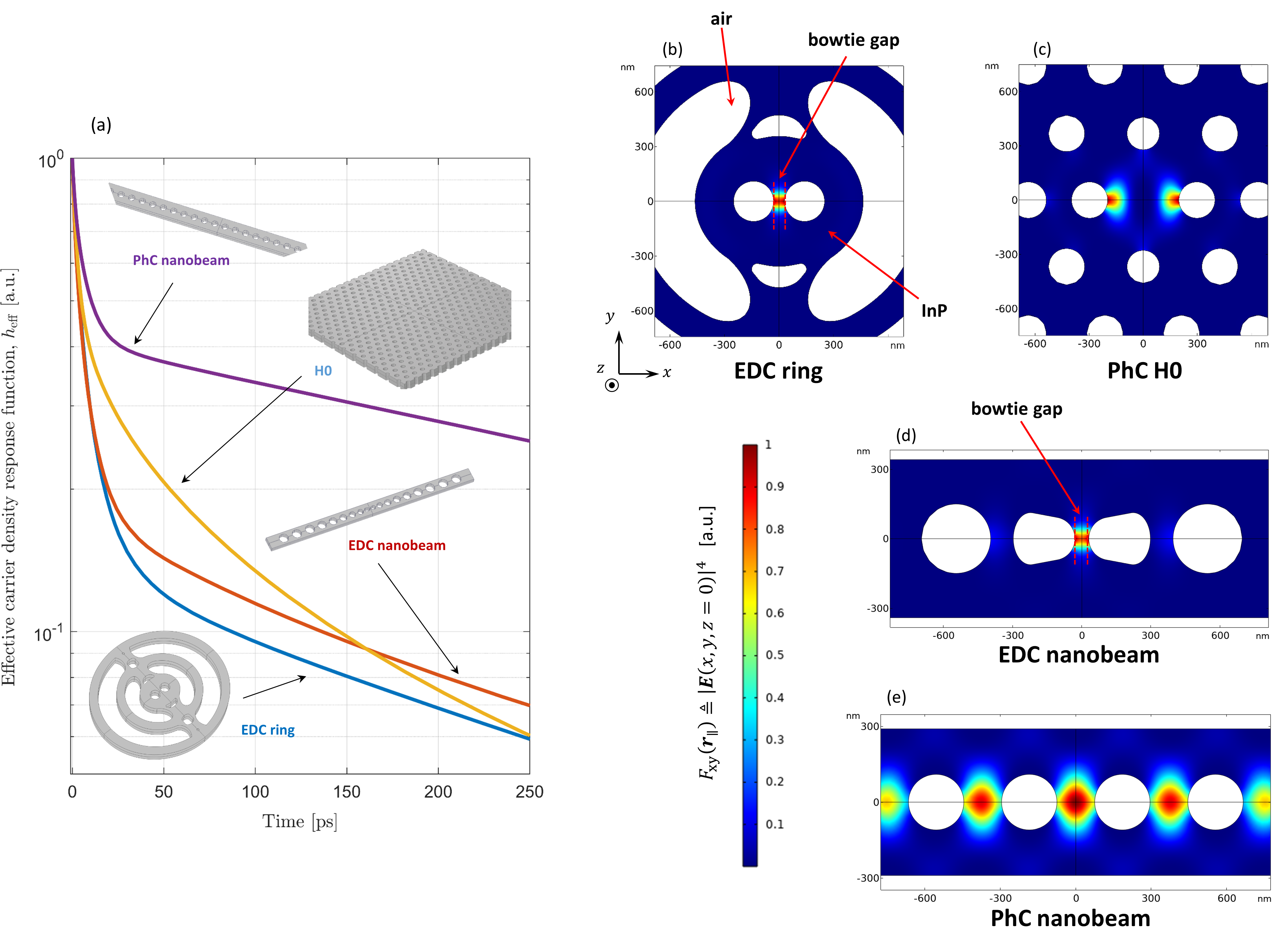
However, the modulation speed is limited by the diffusion and recombination time of the excited carriers, and data transmission rates exceeding a few tens of Gbit/s are yet to be demonstrated Bekele et al. (2019). Previous works Nozaki et al. (2010); Yu et al. (2013); Moille et al. (2016b) on photonic crystal (PhC) cavities Saldutti et al. (2021) have shown that tight field confinement reduces the time it takes for the carriers to diffuse out of the effective mode area of interest. Here, we show that new cavity designs comprising a bowtie and featuring deep sub-wavelength optical confinement Hu and Weiss (2016); Choi et al. (2017); Wang et al. (2018); Albrechtsen et al. (2022) (so-called extreme dielectric confinement, EDC) further speed up the diffusion of carriers. The large quality factor (Q-factor) and enhanced carrier diffusion may lead to energy-efficient optical switches with superior modulation speeds.
The diffusion and recombination of carriers are often modeled by rate equations, with different numbers of time constants Johnson et al. (2006); Heuck et al. (2013); Yu et al. (2013). The time constants are usually determined by fitting to experiments or space- and time-domain simulations of the ambipolar diffusion equation Tanabe et al. (2008); Nozaki et al. (2010); Yu et al. (2013). However, it has been pointed out that even a multi-exponential decay may not be entirely satisfactory and that a Green’s function formalism generally provides better accuracy Moille et al. (2016b). The Green’s function of the mode-averaged (or effective) carrier density reflects the shift in the cavity resonance due to an impulse excitation of carriers in the time domain. Fig. 1a shows the Green’s function - from now on, response function - of the effective carrier density for the cavities considered in this article: EDC ring (blue), EDC nanobeam (red), PhC H0 (yellow), and PhC nanobeam (purple). The cavity parameters are summarized in Tab. 1. The in-plane excitation profile of the carrier density due to two-photon absorption is illustrated in Fig. 1b, c, d and e.
In Tab. 1, in addition to the geometrical parameters (in-plane footprint and cavity thickness), we include the quality factor (Q-factor), as well as the two-photon absorption (TPA) and free-carrier absorption (FCA) mode volume Saldutti et al. (2021). These parameters are computed from three-dimensional simulations of Maxwell’s equations in the frequency domain with radiation boundary conditions Kountouris et al. (2022). In semiconductor nanocavities, the intensity of the carrier generation rate due to TPA and the induced nonlinear losses scale with the inverse of the nonlinear mode volumes, as detailed in Yu et al. (2013). Compared to the PhC cavities, the Q-factor of the EDC cavities in Tab. 1 is relatively low. However, the in-plane footprint of the PhC cavities is much larger. The Q-factor of the EDC cavities could be increased by adding air rings or air holes without altering the geometry in the bowtie proximity Wang et al. (2018). We emphasize that plasmonic resonators also feature deep sub-wavelength optical confinement Schuller et al. (2010). However, the Q-factor of the EDC cavities in Tab. 1 is already much larger than offered by plasmonic cavities Wang and Shen (2006); Khurgin (2015).
The response function in Fig. 1a is obtained from full three-dimensional simulations of the ambipolar diffusion equation in space and time. Surface recombination at the boundaries between the semiconductor material and surrounding air is also included. Compared to more conventional geometries, the electric field in EDC cavities is tightly localized to a hot spot, which accelerates the effective carrier density decay rate. As discussed later, further improvements are feasible by scaling down the bowtie gap.
However, depending on the timescale of interest, time-domain simulations may be computationally demanding. Furthermore, three-dimensional simulations tend to obscure the impact of the cavity geometry in the -plane (in-plane) and along the growth direction, (out-of-plane). The -, - and -directions are indicated in Fig. 1b.
In this article, we present an alternative eigenmode expansion technique to calculate the response function of the effective carrier density. This eigenmode approach efficiently provides the long-timescale decay rate with only a few eigenmodes of the ambipolar diffusion equation. Notably, the eigenmode approach singles out the contributions of the in-plane and out-of-plane diffusion dynamics, thus offering new insights, that will guide future cavity designs, e.g., by topology optimization Jensen and Sigmund (2011); Molesky et al. (2018).
The article is organized as follows. Sec. II introduces the carrier diffusion model. In particular, the approximations leading from the drift-diffusion model to the ambipolar diffusion regime are illustrated step by step, and the limitations are discussed, including the impact of surface recombination. The eigenmode expansion and response function formalism are presented in Sec. III. The eigenmode approach is then applied in Sec. IV and Sec. V, respectively, to analyze the in-plane and out-of-plane diffusion dynamics in detail, with an overview of the cavities in Tab. 1. Finally, Sec. VI draws the main conclusions.
| Cavity | Q-factor | In-plane footprint | Cavity thickness | ||
|---|---|---|---|---|---|
| EDC ring | 0.5 | 0.3 | , (ellipse axes) | 240 | |
| EDC nanobeam | 0.8 | 0.5 | 250 | ||
| PhC H0 | 1.7 | 1 | 340 | ||
| PhC nanobeam | 3 | 2 | 250 |
II Carrier diffusion model: from drift-diffusion to ambipolar diffusion
The drift-diffusion equations are pivotal for understanding fundamental characteristics of electronic and photonic devices, including transistors Sze and Ng (2006), photodetectors Liu (2005) and solar cells Nelson (2003), and have also been applied to semiconductor lasers Tessler and Eistenstein (1993); Gready and Eisenstein (2013); Tibaldi et al. (2019); Saldutti et al. (2020), for cases where simpler descriptions based on rate equations may be inadequate. For instance, effects such as the quenching of the ground-state power in the presence of dual-state lasing, or the impact of p-type modulation doping on the lasing threshold are naturally explained Saldutti et al. (2020) within a drift-diffusion picture.
The optical switching characteristics of semiconductor nanocavities are well understood in a modeling framework that combines temporal coupled-mode theory with the ambipolar regime of the drift-diffusion equations Nozaki et al. (2010); Yu et al. (2013); Moille et al. (2016a). However, the literature is not always clear on the approximations involved, and conflicting descriptions flourish, especially regarding the recombination terms. In the following, we derive the ambipolar diffusion equation from the classical drift-diffusion equations, outlining the main approximations and limitations.
The drift-diffusion model Vasileska et al. (2010) consists of the continuity equations for electrons and holes, typically coupled to Poisson’s equation. Carrier heating effects Mark and Mørk (1992) are ignored, assuming that the excited electrons and holes have already relaxed to their quasi-equilibrium distributions, described by quasi-Fermi levels. The approximation is appropriate on timescales longer than about Moille et al. (2016b), to which the conclusions of this article are therefore restricted. The continuity equations read
| (1a) | ||||
| (1b) | ||||
Here, and are the densities per unit volume of electrons and holes, respectively, whereas is the electron charge. The electron () and hole () current density per unit area reflects the motion of electrons and holes and accounts for both drift and diffusion.
The generation rates per unit volume and unit time describe the excitation of excess electrons () and holes () with respect to thermal equilibrium. We assume optical excitation, which is fast compared to the timescales of the other processes. Therefore, electrons and holes are generated in pairs, leading to the same generation rate, .
The recombination rates per unit volume and unit time of electrons () and holes () account for trap-assisted recombination in the bulk semiconductor material, as well as radiative and Auger recombination. At carrier densities around , as relevant Borghi et al. (2021) for optical switching applications, trap-assisted recombination usually dominates over radiative and Auger recombination Moille et al. (2016b, 2017), which are characterized by longer lifetimes.
Trap-assisted recombination deserves special consideration. Strictly speaking, it is only under steady-state conditions that the general theory Shockley and Read (1952) of electron and hole trap-assisted recombination reduces to the well-known Shockley-Read-Hall (SRH) recombination rate Shockley and Read (1952); Hall (1952); Pierret (2002)
| (2) |
with and given by
| (3a) | ||||
| (3b) | ||||
Here, is the electron and hole intrinsic concentration, is the intrinsic Fermi level and is the trap energy level, including the trap degeneracy factor Pierret (2002). A single trap level dominates trap-assisted bulk recombination Pierret (2002). The Boltzmann constant and temperature are denoted by and , respectively. In Eq. 2, the probability per unit time of an electron (hole) being trapped when the traps are all empty is (). This probability is inversely proportional to the density of traps per unit volume.
In general, electrons and holes feature different capture cross-sections, which leads to under time-varying conditions Shockley and Read (1952); Blakemore (1962). As a result, an electron (or hole) may be trapped for a certain period before recombining, which tends to unbalance the electron and hole densities. Recent works on nano-waveguides Aldaya et al. (2017) and microring resonators Novarese et al. (2022) have pointed out that modeling the electron and hole recombination rates with separate formulations Blakemore (1962) is necessary to accurately reproduce the nonlinear carrier dynamics observed experimentally. In particular, the carrier decay rate due to trap-assisted recombination generally depends on the initial carrier density Ahrenkiel et al. (1991); Aldaya et al. (2017), which makes the process nonlinear.
In practice, one may assume if the dynamics of the trapped electrons and holes is sufficiently slow compared to the drift-diffusion dynamics, and, in general, to the timescale of interest Pierret (2002); Vasileska et al. (2010). This quasi-stationary approximation is justified when the trap density is small compared to the excess electron and hole densities Aldaya et al. (2017), and typically satisfactory at carrier densities around Borghi et al. (2021), which we are interested in. Furthermore, the carrier lifetimes due to trap-assisted recombination are typically larger than Aldaya et al. (2017); Novarese et al. (2022). This further corroborates the quasi-stationary approximation on much shorter timescales, where carrier diffusion is expected to dominate. Trap-assisted recombination due to defects at the interface between the semiconductor material and surrounding cladding (so-called surface recombination) Pierret (2002) is discussed later, but similar considerations can be made.
We consider photonic cavities realized using semiconductor materials that are either intrinsic or homogeneously doped. Therefore, without an external excitation, the electron and hole densities are uniform throughout the cavity. In the presence of an optical excitation pulse, electrons and holes are generated and initially diffuse at different speeds, due to the different mobilities. Electrons and holes, however, are charged particles. As a result, an internal electric field arises, which tends to retard the electrons and accelerate the holes McKelvey (1966). If trap-assisted recombination does not unbalance the electron and hole densities (an assumption whose limitations have been discussed above), the internal electric field ensures local neutrality. This means that the excess electron density is balanced by an equal excess hole density. Consequently, electrons and holes end up diffusing together, in a so-called ambipolar diffusion regime van Roosbroeck (1953).
It is clear that if local neutrality were fulfilled exactly, no internal field would be set up. However, the difference between electron and hole densities required to induce the internal field is so small compared to the excess densities themselves, that local neutrality is often a good approximation McKelvey (1966).
Assuming local neutrality, we denote by the excess density of electrons and holes. We multiply Eq. 1a by and Eq. 1b by , with and being the hole and electron mobility, respectively. Summing the two equations and using Einstein’s relations for the electron and hole diffusion coefficients, we arrive at McKelvey (1966)
| (4) |
where the effective diffusion coefficient, , is
| (5) |
and the effective mobility, , reads
| (6) |
Here, () is the electron (hole) density at thermal equilibrium (with and ), whereas and are the electron and hole diffusion coefficient, respectively. The electric field, , accounts for the internal field and any externally applied bias. The external field is assumed to be weak enough that the ambipolar approximation would hold. Eq. 4 is the basis of the classical Haynes-Shockley experiment to measure the minority carrier mobility in n- or p-type semiconductors Haynes and Shockley (1951); McKelvey (1956).
We assume high-level injection, whereby the excess electron and hole density is much larger than the thermal equilibrium concentrations. This is the typical scenario for lasing Coldren et al. (2012) and optical switching Nozaki et al. (2010); Yu et al. (2013); Moille et al. (2016a) applications unless the semiconductor material is heavily doped Moille et al. (2017). For the sake of reference, we note that the room-temperature equilibrium carrier concentration of intrinsic indium phosphide is around Levinshtein et al. (1998). We also assume no externally applied bias. Therefore, reduces to the internal field. For , Eq. 6 gives , whereas Eq. 5 reduces to
| (7) |
As for the SRH recombination rate, it should be noted that unless the trap level is close enough to the intrinsic Fermi level (around the middle of the electronic band gap), either or will become large, significantly reducing the recombination rate. For the traps to be effective, they must introduce energy levels close to the middle of the gap Coldren et al. (2012), in which case one finds . Thus, Eq. 2 under high-level injection gives Coldren et al. (2012)
| (8) |
with being the recombination lifetime. Consequently, Eq. 4 reduces to the usual form of the ambipolar diffusion equation McKelvey (1966); Yu et al. (2013); Moille et al. (2016b)
| (9) |
with the effective diffusion coefficient given by Eq. 7.
The drift-diffusion equations require suitable boundary conditions. In particular, surface recombination due to interface traps (so-called surface states) should be modeled, in general, via the following boundary conditions Engl et al. (1983); Mui and Coldren (1995)
| (10a) | |||
| (10b) | |||
Here, and are the electron and hole surface recombination rates per unit area, respectively, whereas is the unit vector normal to the semiconductor surface and pointing outwards.
The physical analogies between trap-assisted bulk recombination and surface recombination lead to similar considerations and mathematical descriptions. The density of surface states, however, is naturally expressed as a density per unit area, because interface defects are spread throughout a plane rather than a volume. As a consequence, () in Eq. 2 becomes (), with and being the electron and hole surface recombination velocity, respectively. These velocities are directly proportional to the electron and hole capture cross-sections, respectively, as well as the density of surface states. If the dynamics of the electrons and holes trapped at the surface states is sufficiently slow, the surface recombination rates for electrons and holes are the same. Then, for a single trap energy level, one finds Pierret (2002)
| (11) |
where and are the electron and hole densities per unit volume at the semiconductor surface, respectively. The expressions of and are given by Eq. 3a and Eq. 3b, respectively, but the intrinsic Fermi level and the intrinsic carrier density are evaluated at the surface. The trap level is that of the surface states.
It should be noted that surface recombination usually involves trap levels distributed in energy throughout the electronic band gap Pierret (2002), in contrast to bulk recombination. Therefore, one should in principle integrate Eq. 11 over all the trap levels, with possibly energy-dependent surface recombination velocities Pierret (2002). However, the recombination process is dominated by trap levels close to the middle of the gap, as already noted for bulk recombination. Therefore, one may often assume constant surface recombination velocities, equal to the midgap value Schenk (1998). Then, under the assumption of high-level injection, Eq. 11 reduces to Coldren et al. (2012)
| (12) |
where is the excess electron and hole density at the semiconductor surface. The surface recombination velocity, , is given by . It is strongly dependent on the semiconductor material and fabrication process Nolte (1990); Moille et al. (2016a); Black et al. (2017); Higuera-Rodriguez et al. (2017).
To obtain the boundary condition for Eq. 9, we multiply Eq. 10a and Eq. 10b by and , respectively. We subtract the second equation from the first one and express the electron and hole current densities in terms of the corresponding drift-diffusion contributions. We use the ambipolar approximation (namely, and ), as well as , finally arriving at
| (13) |
Here, the excess carrier density is evaluated at the semiconductor surface.
It should be pointed out that surface states usually act as donor-like or acceptor-like recombination centers and possess a charge depending on the occupation Aberle et al. (1992); Mui and Coldren (1995); Donchev et al. (2018). The resulting electric field tends to unbalance the electron and hole densities Mui and Coldren (1995) and should in principle be taken into account by self-consistently coupling the surface recombination rates with Poisson’s equation Girisch et al. (1988); Aberle et al. (1992); Mui and Coldren (1995); McIntosh and Black (2014). The unbalance, however, is minor if the density of surface states is small compared to the excess electron and hole densities Mui and Coldren (1995), and may be neglected, as a first approximation, under high-level injection conditions.
We also note that surface recombination in nanostructures usually dominates over bulk recombination, owing to the large surface-to-volume ratio Dimitropoulos et al. (2005); Higuera-Rodriguez et al. (2017); Aldaya et al. (2017). Therefore, for a given density of surface states, the unbalance between the electron and hole surface recombination rates may eventually become important when the surface-to-volume ratio is sufficiently large Aldaya et al. (2017), and thus jeopardize the ambipolar approximation. This modeling scenario falls outside the scope of this article and is left to future works.
Here, we model the carrier diffusion by Eq. 9, and surface recombination by Eq. 13, consistently with previous works Nozaki et al. (2010); Yu et al. (2013); Moille et al. (2016a). Electrostatic and saturation effects Girisch et al. (1988); Aberle et al. (1992); Mui and Coldren (1995) are ignored, as discussed above. Unless otherwise specified, we assume parameters realistic for Indium Phosphide (InP): Levinshtein et al. (1998) and Yu et al. (2013).
III Eigenmode expansion and response function formalism
In optical switches based on micro- or nanoscale semiconductor resonators, the shift in the cavity resonance due to various carrier-induced effects (mainly, free carrier-induced dispersion) Bennett et al. (1990) scales to first order with a mode-averaged (or effective) carrier density Johnson et al. (2006); Yu et al. (2013):
| (14) |
Here, is the electric field of the cavity mode, is the permittivity and is the semiconductor volume. The integration volume, , encloses the optical cavity with a margin of a few wavelengths. The carrier density, , follows the ambipolar diffusion equation (Eq. 9), with surface recombination boundary conditions (Eq. 13).
It should be noted that the field distribution diverges in space at sufficiently large distances from the cavity, due to the leaky nature of the cavity mode Kristensen et al. (2020). In principle, this divergence makes the denominator of Eq. 14 ill-defined and raises the question of the normalization of the cavity mode Kristensen et al. (2015); Muljarov and Langbein (2017); Kristensen et al. (2017). The choice of , however, does not affect the decay rate of , which makes the issue unimportant for the scope of this article. We also note that the numerator of Eq. 14 is instead well-defined.
In the framework of coupled-mode theory, the carrier generation rate in the diffusion equation is a separable function of space and time Barclay et al. (2005); Moille et al. (2016b):
| (15) |
We focus on optical switches with carriers generated by two-photon absorption (TPA) Barclay et al. (2005); Yu et al. (2013); Moille et al. (2016a). In this case, describes the time variation of the squared optical intensity inside the cavity. The carrier density excitation profile, , is given by
| (16) |
The case of linear absorption, as relevant for semiconductor lasers Coldren et al. (2012), corresponds to . We emphasize that the nonlinear switching dynamics, as analyzed, for instance, in other works Yu et al. (2013); Moille et al. (2016a); Saldutti et al. (2022), is outside the scope of this article, where we focus on the diffusion of carriers. Nonlinear effects on are neglected, and the carrier diffusion model is linear.
The carrier density may be expressed as Moille et al. (2016b)
| (17) |
where is the response function. The response function (see Sec. I in the Supplementary Material) is the solution of the homogeneous diffusion equation
| (18) |
with the initial condition given by .
To gain insight, we postulate a solution in the form
| (19) |
with being the in-plane position vector and the out-of-plane position coordinate. We emphasize that for the solution to be exact, the initial condition should be also separable, namely
| (20) |
This is not generally the case. Nonetheless, as we shall see, this separation procedure provides a good approximation of the effective carrier density.
By inserting Eq. 19 into Eq. 18, the latter is reduced to two eigenvalue problems, corresponding to the in-plane and out-of-plane diffusion dynamics, respectively. By expanding the two solutions on the corresponding sets of eigenmodes (see Sec. II in the Supplementary Material), and averaging over the optical mode profile, one finally arrives at the response function of the effective carrier density
| (21) |
with the effective carrier density given by
| (22) |
Nonlinear effects may be easily included by coupling with the coupled-mode theory equations describing the optical intensity inside the cavity Yu et al. (2013); Moille et al. (2016a).
The response function of the in-plane effective carrier density, , reads
| (23) |
with being the eigenvalues of the in-plane diffusion problem, and the corresponding lifetimes. The excitation coefficients, , are given by
| (24) |
with reading
| (25) |
and being the eigenmodes of the in-plane diffusion problem. is the in-plane cross-section area limited to the semiconductor material. is an in-plane cross-section area enclosing the cavity with a margin of a few wavelengths and including both the semiconductor and surrounding cladding. Similar considerations apply to the denominator of Eq. 24 as to that of Eq. 14. To arrive at Eq. 24, we have also assumed the electric energy density in Eq. 14, , to be a separable function of and , consistently with the initial condition (cf. Eq. 20).
Eigenmodes and eigenvalues are found by solving the diffusion equation in two dimensions via the finite-element method (FEM), and is readily computed by applying Eq. 23. Alternatively, one may find by solving the diffusion equation in space and time Nozaki et al. (2010); Yu et al. (2013); Moille et al. (2016b) and with the initial condition given by . Eq. 23 converges to the result of the latter approach when a sufficiently large number of eigenmodes is considered, as we shall see in Sec. IV.
Similar considerations apply to the response function of the out-of-plane effective carrier density, . Specifically, one finds
| (26) |
with being the out-of-plane diffusion lifetimes. The corresponding excitation coefficients, , are found by applying Eq. 24 and Eq. 25 with obvious changes of the surface integrals into one-dimensional integrals along . In particular, and are replaced by and , respectively, the latter being the out-of-plane eigenmodes. We emphasize that Eq. 26 is a generalization of the usual single-lifetime approximation, , of the out-of-plane diffusion dynamics, with Nozaki et al. (2010); Yu et al. (2013). Here, is the thickness of the cavity, and is the surface recombination velocity. The out-of-plane diffusion dynamics is analyzed in Sec. V.
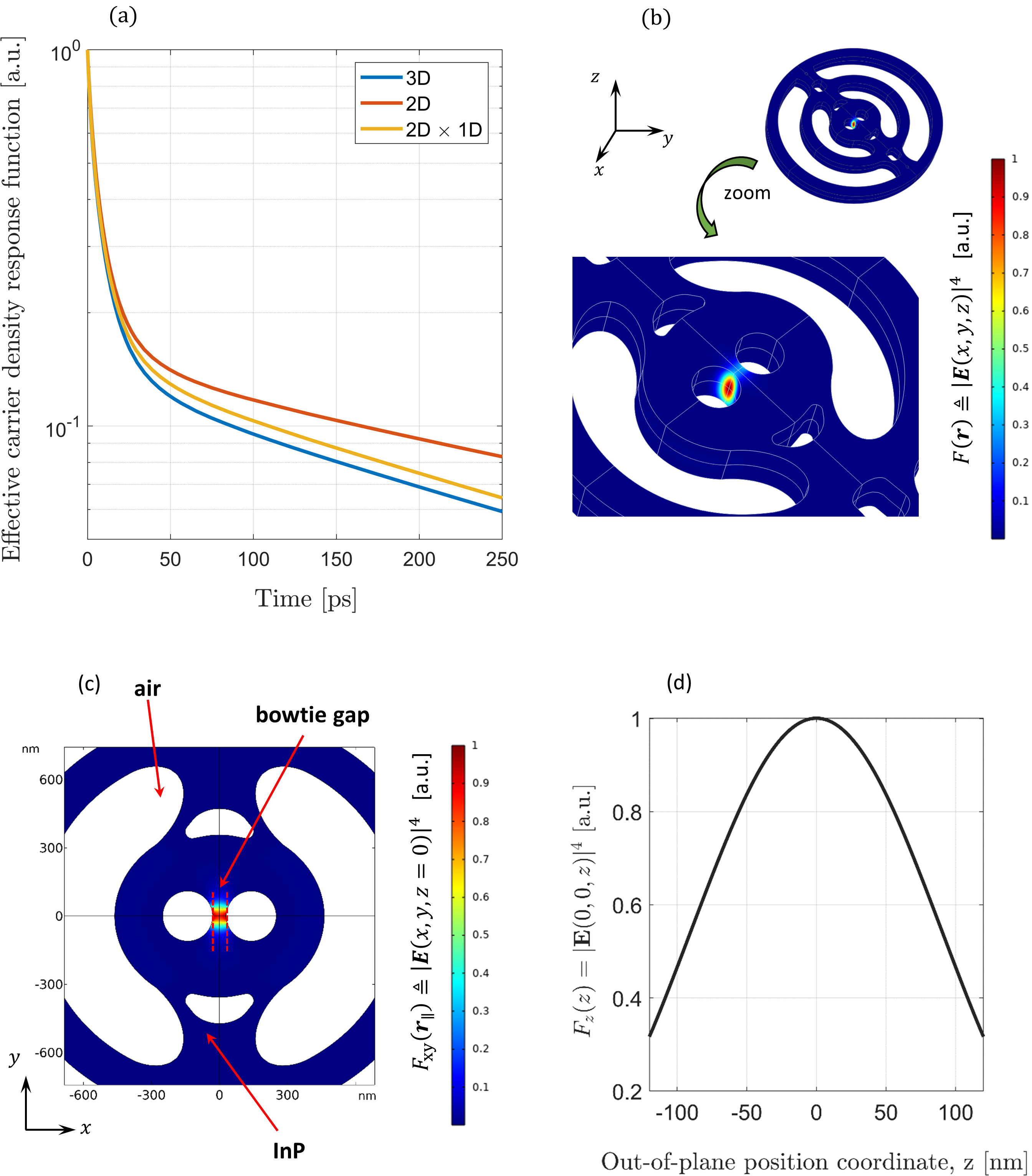
For example, Fig. 2a shows the response function of the effective carrier density for the EDC ring cavity in Tab. 1. The excitation profile, , is displayed in Fig. 2b. The electric field corresponds to the cavity fundamental mode. It is obtained from three-dimensional FEM simulations of the source-free Maxwell’s equations in the frequency domain with radiation boundary conditions Kountouris et al. (2022). The excitation profile over the in-plane cross-section area () and along the cavity growth direction, , at the center of the cavity () is shown in Fig. 2c and Fig. 2d, respectively. To focus on the effect of carrier diffusion, bulk recombination is ignored (). The curves in Fig. 2a correspond to full three-dimensional simulations (blue), two-dimensional simulations of the in-plane diffusion (red, Eq. 23), and combined simulations of the in-plane and out-of-plane diffusion (yellow, Eq. 21). In three dimensions, the response function is found from space- and time-domain simulations, but the eigenmode approach could be also applied (see Sec. I in the Supplementary Material).
From Fig. 2a, the separation into in-plane and out-of-plane diffusion (2D1D, yellow) is seen to be a good approximation of the full three-dimensional dynamics (3D, blue). The out-of-plane diffusion mainly affects the long-timescale decay rate. The separation of the excitation profile, Eq. 20, is fulfilled only approximately, which explains the non-perfect agreement between Eq. 21 and the three-dimensional simulation results.
For the other photonic cavities, we have found similar results. We note that the fundamental mode profile of PhC H0 cavities features a node at the center of the cavity (see Fig. 1c). However, the separation procedure herein illustrated is still applicable by choosing the in-plane position coordinates, and , around a maximum of the field profile when considering .
IV In-plane diffusion
In the following, we focus on the contribution to the carrier dynamics due to in-plane diffusion.
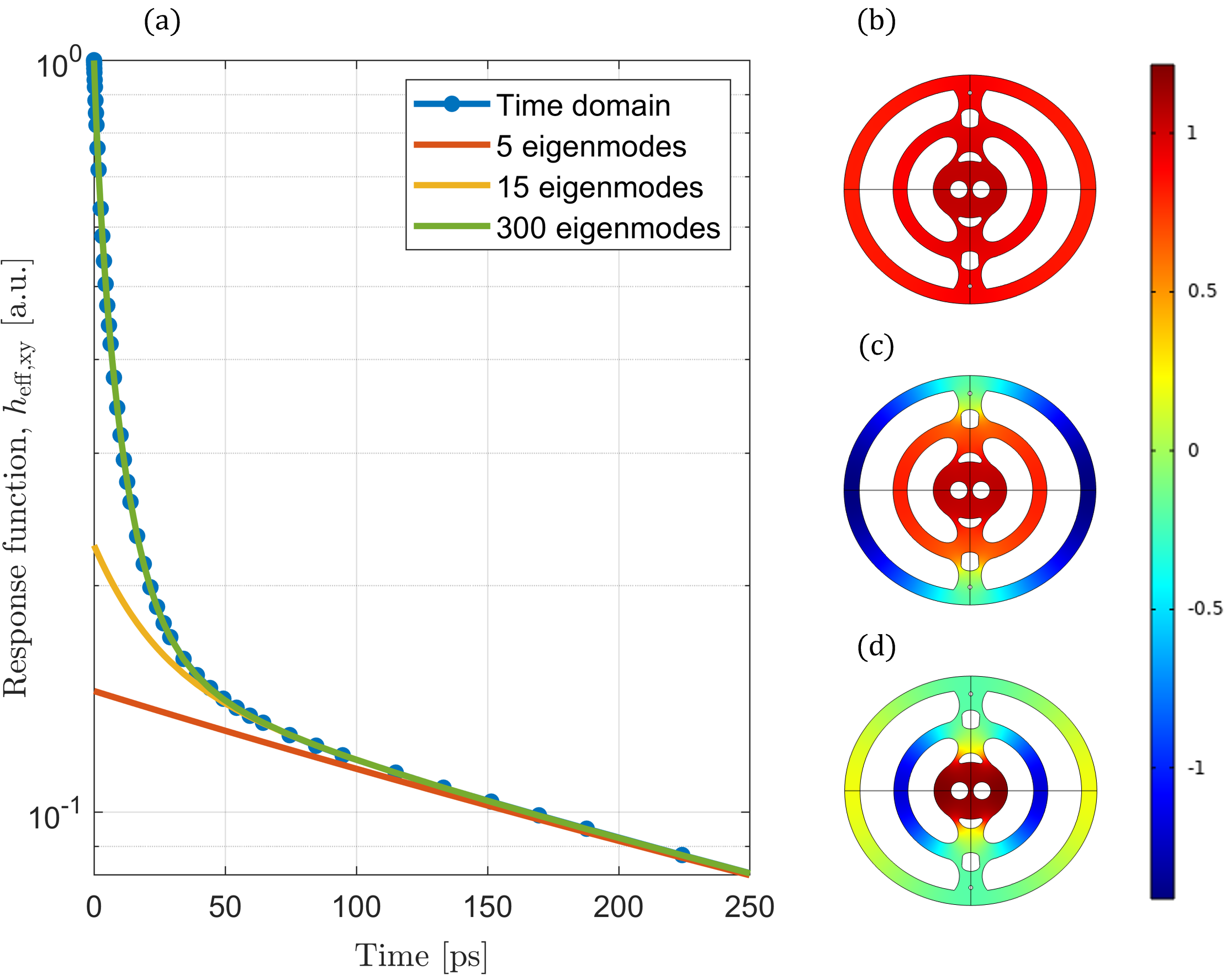
Fig. 3a shows the response function of the in-plane effective carrier density for the EDC ring cavity in Tab. 1, as obtained from space- and time-domain simulations (blue) and applying the eigenmode expansion introduced in Sec. III. Here, we have sorted the eigenmodes by decreasing values of the diffusion lifetimes and accounted for the first 5 (red), 15 (yellow), and 300 eigenmodes (green). For example, the first three eigenmodes are shown in Fig. 3b, c and d, respectively. The eigenmode approach conveniently captures the long-timescale decay rate with only a few eigenmodes, which is advantageous compared to time-domain simulations. Empirically, we have found that around eigenmodes are generally enough to calculate the response function at all times. This criterion applies to all the photonic cavities considered in this article. Moreover, as we shall see, sorting the eigenmodes by different criteria may reduce the number of eigenmodes being required.
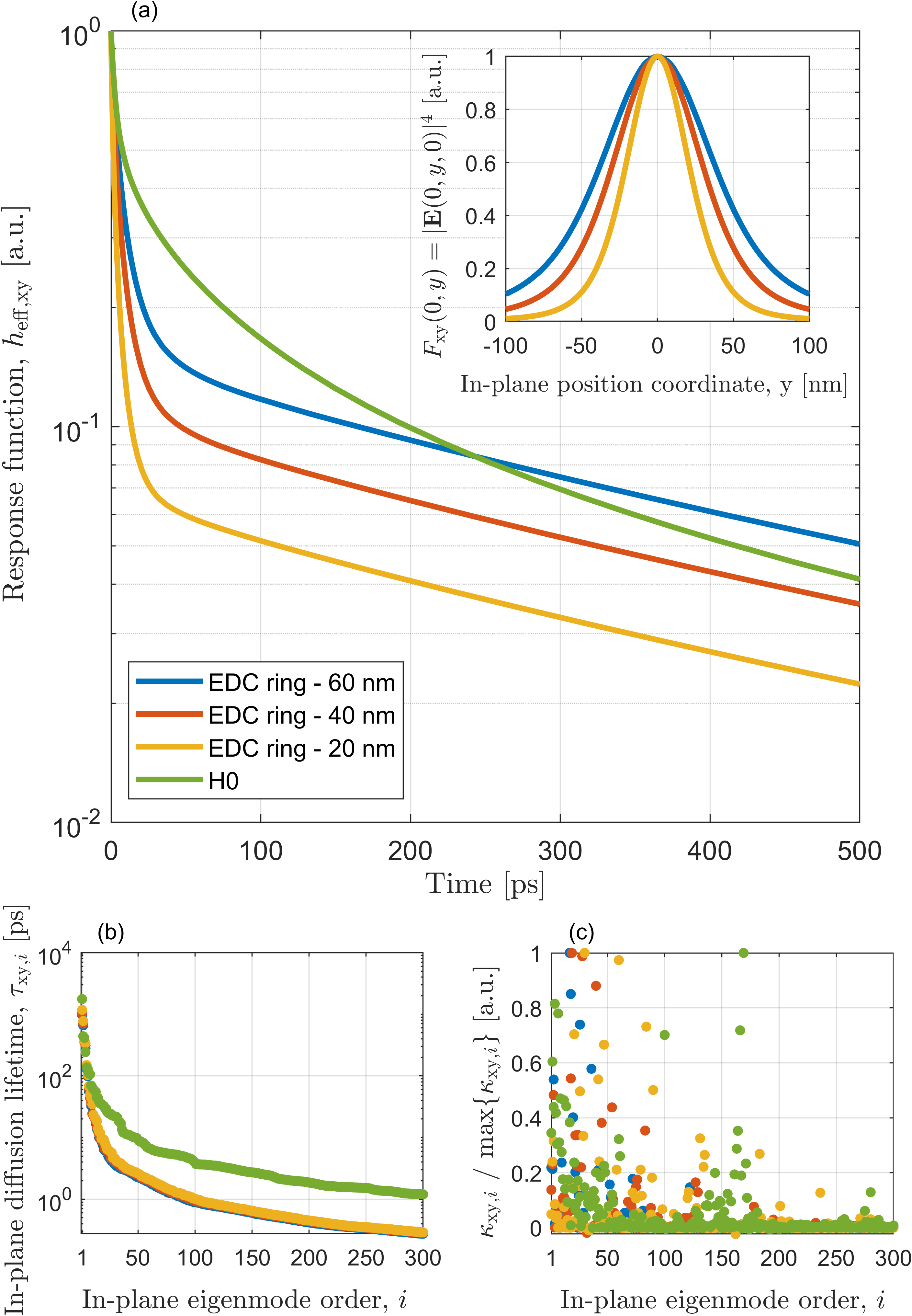
As shown in Fig. 1a, tighter field confinement accelerates the decay rate of the effective carrier density. Therefore, exploring the impact of the bowtie gap in EDC cavities is interesting. For this purpose, Fig. 4a displays the response function of the in-plane effective carrier density for the PhC H0 cavity (green) and EDC ring cavity in Fig. 1. The bowtie gap is (blue), (red) and (yellow). We note that even smaller values have been demonstrated both in Silicon Albrechtsen et al. (2022) and InP Xiong et al. (2023). Scaling down the bowtie gap accelerates the decay rate on the short timescale. We emphasize that a smaller bowtie gap does not only squeeze the field along the -direction (for the reference system, see Fig. 1b), but also along the -direction, as illustrated in the inset of Fig. 4a.
Unfortunately, direct inspection of the diffusion lifetimes, (Fig. 4b), or the excitation coefficients, (Fig. 4c), does not elucidate further the role of the bowtie gap. Furthermore, the size of the bowtie gap barely affects the TPA and FCA mode volumes (not shown). This observation signifies that these mode volumes are not a direct measure of the carrier diffusion enhancement.
To gain insight, we introduce the in-plane instantaneous lifetime, , defined as follows:
| (27) |
In particular, by inserting the eigenmode expansion from Eq. 23, one finds
| (28) |
For , the instantaneous lifetime reduces to the longest lifetime, , which supports the definition. At a generic time, the inverse of the instantaneous lifetime gives the exponential decay rate of the effective carrier density.
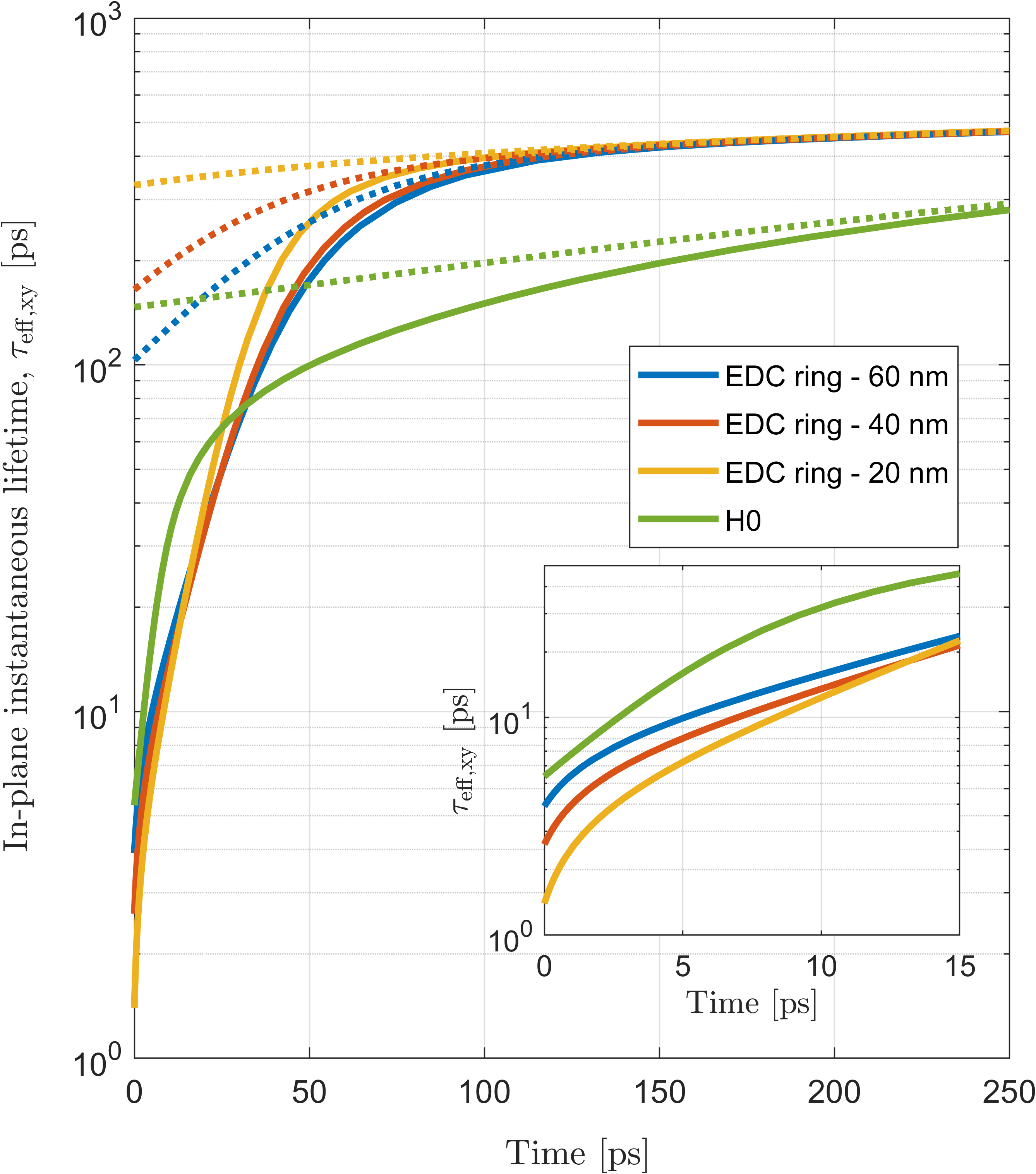
Fig. 5 shows the instantaneous lifetime versus time for the PhC H0 cavity (green) and EDC ring cavity. Again, the bowtie gap is (blue), (red) and (yellow). Including only a few eigenmodes with the longest diffusion lifetime (dotted) is enough to calculate the instantaneous lifetime on the long timescale, as expected. We also note that the diffusion lifetimes decrease with increasing surface recombination velocity (not shown). Consequently, for larger surface recombination velocities even fewer eigenmodes are enough to capture the long-timescale decay rate. Zooming on the short timescale (inset) highlights that a smaller bowtie gap reduces the instantaneous lifetime, which is consistent with Fig. 4a. Furthermore, compared to the PhC H0 cavity, the EDC cavities feature shorter instantaneous lifetimes on the short timescale due to the tighter field confinement. The H0 cavity, on the other hand, is faster on the long timescale, most likely due to the larger area exposed to surface recombination.
It is instructive to consider the instantaneous lifetime at zero time:
| (29) |
From here, it is evident that not the lifetimes themselves, but instead a weighted average of the (inverse) lifetimes determines the instantaneous lifetime, with weights given by the excitation coefficients. This explains why considering either the lifetimes or the excitation coefficients alone (see Fig. 4b and Fig. 4c) does not emphasize the impact of the geometry on the carrier diffusion dynamics. Furthermore, Eq. 29 suggests that sorting the eigenmodes by their excitation coefficients may be advantageous on the short timescale.
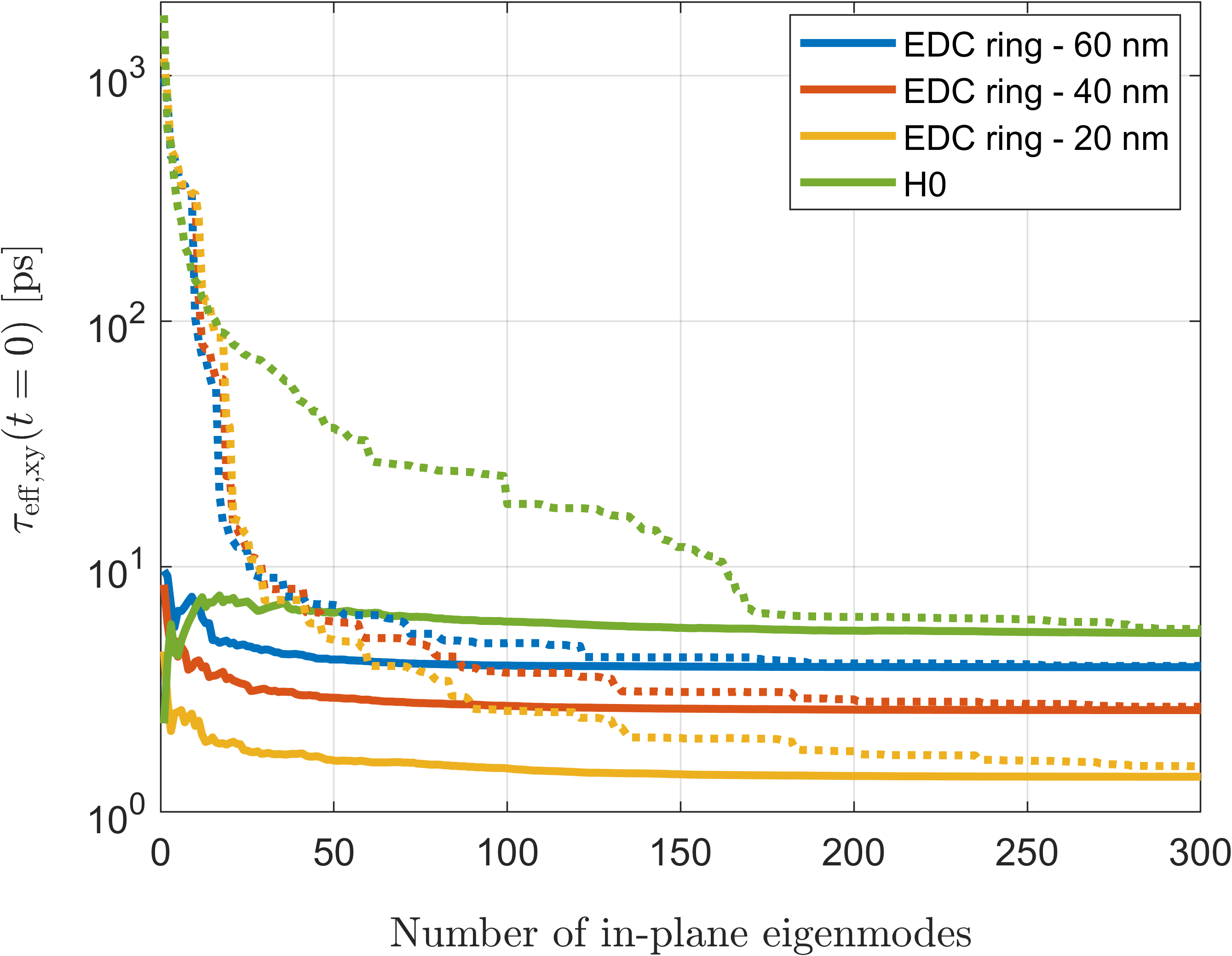
This is evident from Fig. 6, showing the instantaneous lifetime at zero time versus the number of eigenmodes taken into account. Sorting the eigenmodes by decreasing values of (solid) reduces the number of eigenmodes to be included for an accurate estimate. In contrast, sorting the eigenmodes by decreasing diffusion lifetimes (dotted) significantly slows down the convergence. We note that sorting the eigenmodes by increasing diffusion lifetimes (not shown) is not advantageous either. In fact, the diffusion lifetimes monotonically decrease with increasing order of the eigenmodes (see Fig. 4b). Therefore, high-order eigenmodes may easily have diffusion lifetimes much smaller than the instantaneous lifetime at zero time.
To further quantify the impact of the in-plane geometry, we consider the response of the effective carrier density in the presence of in-plane diffusion only:
| (30) |
In particular, we assume the time variation, , of the squared optical intensity inside the cavity to be Gaussian
| (31) |
with full width at half maximum (FWHM) given by
| (32) |
In this case, the in-plane effective carrier density, , can be computed analytically:
| (33) |
with the two time-domain factors, and , given by
| (34a) | ||||
| (34b) | ||||
Here, is the error function, . We note that the intracavity excitation pulse, , only matches the external input pulse if the duration of the latter is much longer than the cavity photon lifetime, as determined by the loaded Q-factor.
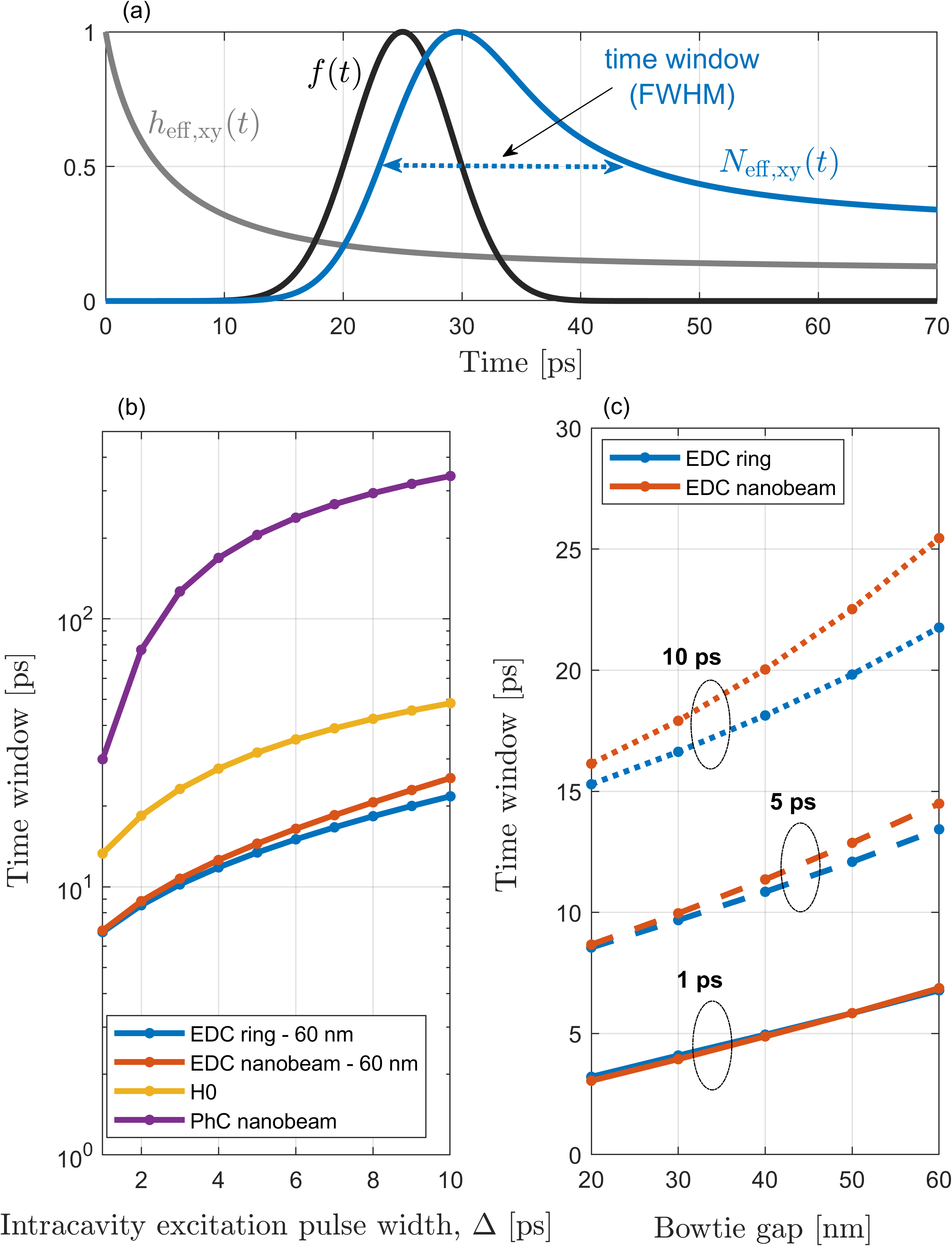
As an example, Fig. 7a shows the time evolution of the in-plane effective carrier density (blue) in response to an intracavity Gaussian excitation (black) with FWHM of . The EDC ring cavity in Tab. 1 is considered, and the corresponding response function (grey) is also shown. The time window (FWHM) of the effective carrier density (cf. Fig. 7a) is reported in Fig. 7b as a function of the intracavity excitation pulse width. On this timescale, the impact of out-of-plane diffusion is safely negligible, as shown in Sec. V. We note that the switching time (FWHM of the cavity transmission) Nozaki et al. (2010); Yu et al. (2013); Ono et al. (2020); Guo et al. (2022) is a critical figure of merit in optical switching applications, and is also influenced by nonlinear effects Yu et al. (2014), herein neglected. Yet, a faster linear response generally reduces the switching time. Therefore, Fig. 7b suggests that EDC cavities (blue and red) may offer shorter switching times than H0 (yellow) or nanobeam (purple) PhC cavities. Despite the differences in the geometry surrounding the bowtie, the two types of EDC cavities show comparable responses due to the similar field hot spots (see Fig. 1b and Fig. 1d).
In addition, shrinking the bowtie gap may further reduce the switching time, as suggested by Fig. 7c. Here, the time window of the effective carrier density in EDC ring cavities (blue) and EDC nanobeam cavities (red) decreases with the bowtie gap. As a reference, we note that switching times measured for optical switches based on PhC H0 cavities are on the order of - Nozaki et al. (2010); Yu et al. (2013).
So far, we have assumed a surface recombination velocity of , representative of InP Yu et al. (2013). However, this parameter is strongly influenced by the semiconductor material and fabrication process. For instance, the surface recombination velocity may be intentionally increased by growing surface quantum wells on InP photonic cavities Bazin et al. (2014a) or by ion implantation in silicon cavities Tanabe et al. (2007). Compared to InP, other materials, such as Gallium Arsenide Moille et al. (2016a), may feature much higher surface recombination velocities. On the other hand, surface passivation techniques have proved effective in limiting surface recombination Black et al. (2017); Higuera-Rodriguez et al. (2017).
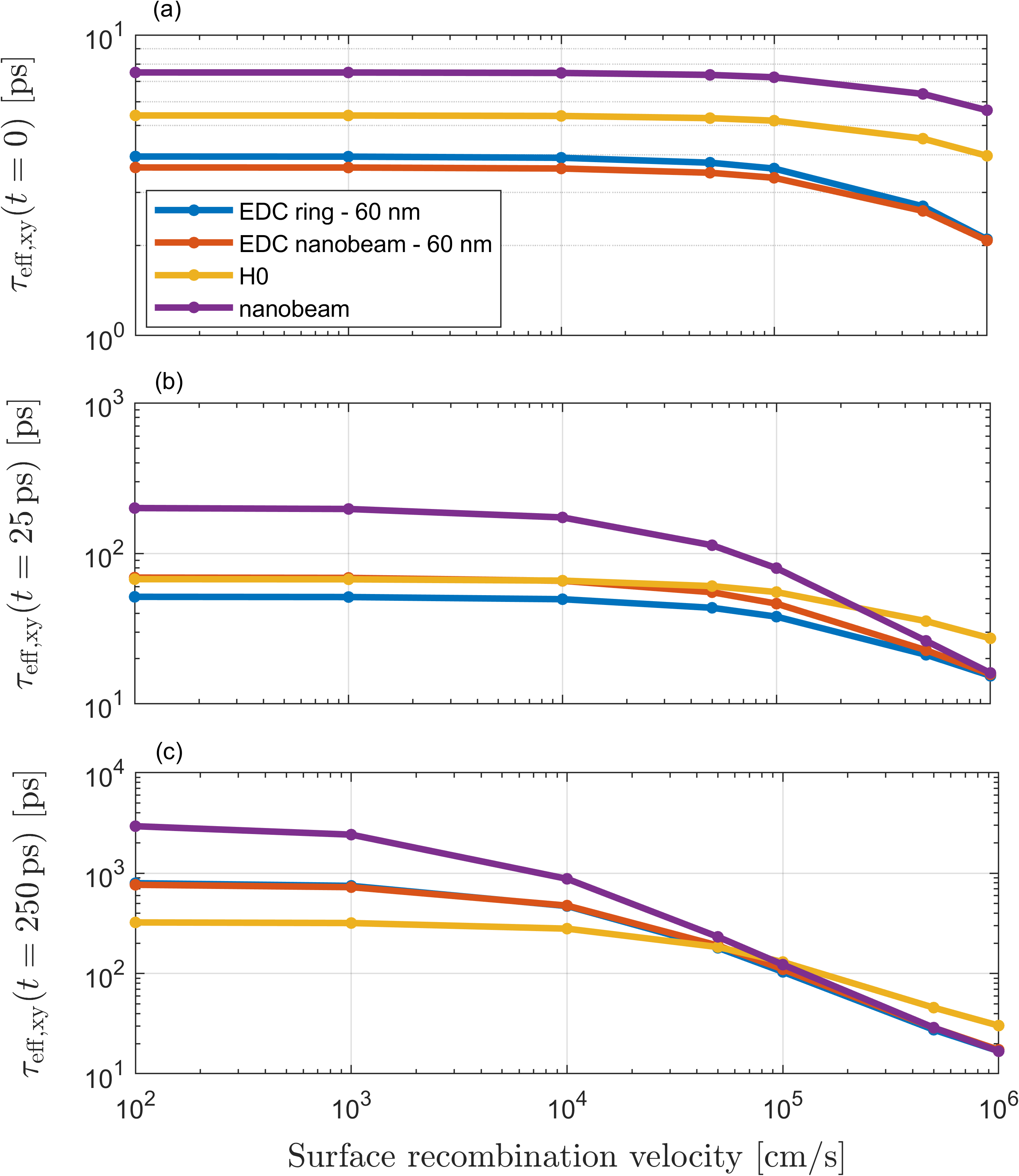
Fig. 8 explores the impact of surface recombination by showing the in-plane instantaneous lifetime at (a) zero time, (b) and (c) as a function of the surface recombination velocity. The different colors correspond to the same cavities as in Fig. 7b. For all cavities, the instantaneous lifetime at zero time hardly depends on the surface recombination velocity. This signifies that the carrier diffusion speed is dominated, in the initial stage, by the excitation spatial profile. A stronger dependence on surface recombination is observed with increasing time as diffusion gradually smears out the initial spatial distribution of the carrier density. On the short timescale (Fig. 8a and Fig. 8b), EDC cavities are generally faster than conventional geometries. Consistently with Fig. 5, PhC H0 cavities may offer higher decay rates at longer times (Fig. 8c), but the advantage fades with increasing surface recombination. Interestingly, we also note that sufficiently large values of surface recombination lead, at sufficiently long times (Fig. 8b and Fig. 8c), to the same carrier decay rate in the EDC cavities and PhC nanobeam cavities. This is because the carrier diffusion essentially reduces to a one-dimensional phenomenon, with similar diffusion lengths in the EDC and PhC nanobeam cavities herein considered. The effect is further discussed in Sec. V in connection with Fig. 11.
We emphasize, though, that large values of surface recombination velocity are not necessarily advantageous for optical switching applications Moille et al. (2016a). Indeed, if the carrier diffusion dynamics is much faster than the excitation pulse, the carriers decay before the optical intensity in the cavity has built up significantly. As a result, the nonlinear change in the cavity transmission is weak, and the switching contrast degrades. For a given input power, the switching contrast is optimal when the duration of the excitation pulse matches the short-timescale carrier dynamics Saldutti et al. (2022).
V Out-of-plane diffusion
In the following, we analyze the contribution to the carrier dynamics due to out-of-plane diffusion. In contrast to the case of in-plane diffusion, the out-of-plane diffusion lifetimes and eigenmodes are described by simple analytical formulas thanks to the one-dimensional nature of the problem.
The out-of-plane diffusion lifetimes, , are given by
| (35) |
where obeys the following equation (see Sec. II in the Supplementary Material):
| (36) |
Here, is the cavity thickness along the cavity growth direction, and the surface recombination velocity, , is the same at the top and bottom surface of the cavity.
The diffusion lifetimes and the excitation coefficients, , determine the response function of the out-of-plane effective carrier density, (cf. Eq. 26). The excitation coefficients are given by
| (37) |
with being the out-of-plane eigenmodes, and reading
| (38) |
The integration line, , in Eq. 37 includes the whole thickness of the cavity, with a margin of a few wavelengths on the top and bottom. Again, similar considerations apply to the denominator of Eq. 37 as to that of Eq. 14.
In analogy to Eq. 27, we introduce the out-of-plane instantaneous lifetime, . From the eigenmode expansion, we obtain
| (39) |
We emphasize that Eq. 36 and Eq. 38 should be generalized if the cavity geometry is not -symmetric or the surface recombination velocity differs at the top and bottom surface of the cavity. This general case is treated later on in this section.
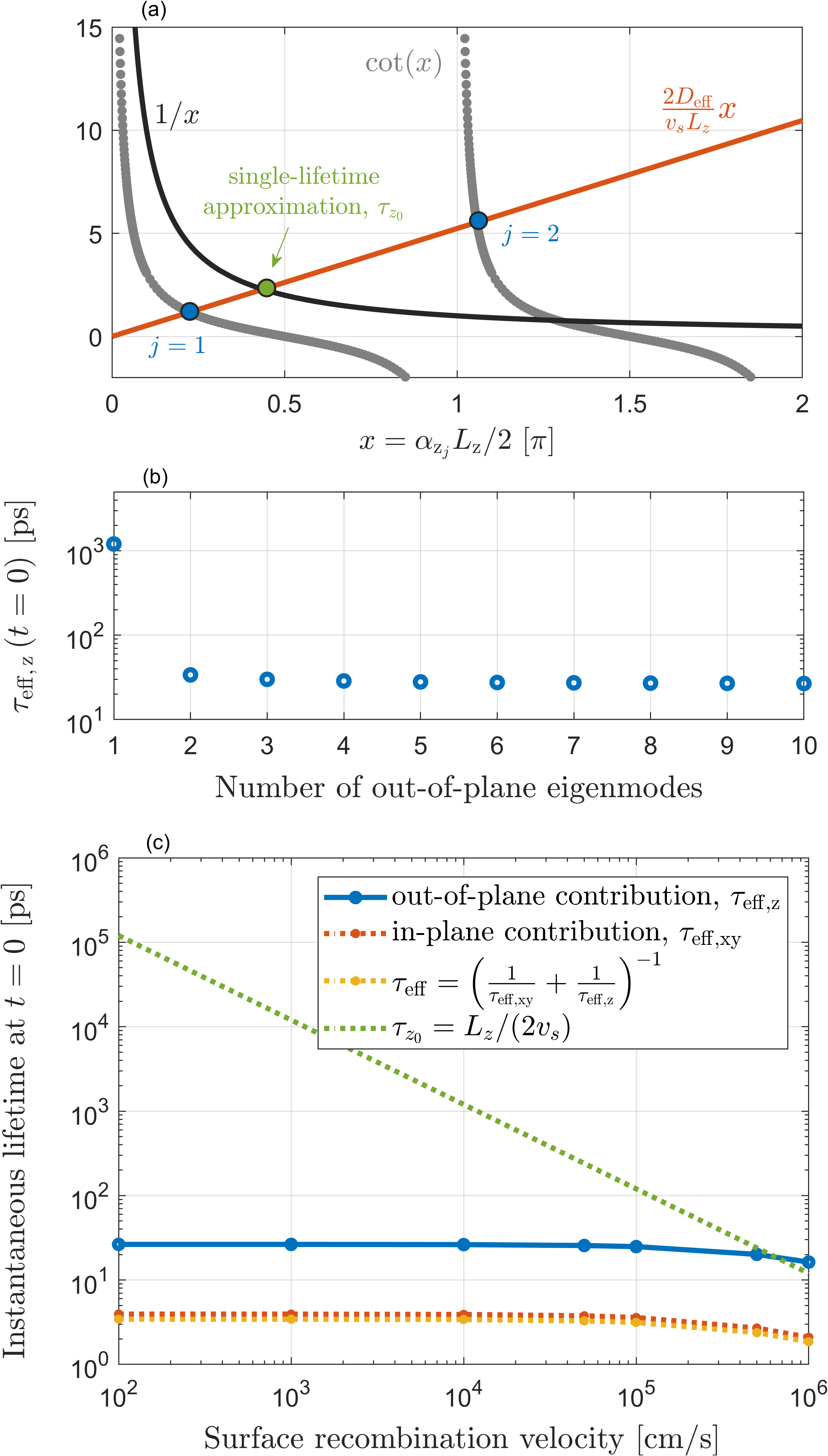
The graphical solution of Eq. 36 is illustrated in Fig. 9a. The intersections (blue bullets) between the straight line (red) on the right-hand side of Eq. 36 and the cotangent function (grey) on the left-hand side determine the values of , and hence the diffusion lifetimes. With decreasing cavity thickness and surface recombination velocity, the intersection corresponding to the longest diffusion lifetime moves closer to the -axis origin, where the cotangent function may be approximated with a hyperbola (black). By inserting in Eq. 36, one recovers the usual single-lifetime approximation Nozaki et al. (2010); Yu et al. (2013)
| (40) |
corresponding to the intersection (green bullet) between the straight line and the hyperbola in Fig. 9a.
Several eigenmodes generally contribute to the instantaneous lifetime, as already seen for the in-plane diffusion. For example, we consider the EDC ring cavity in Tab. 1 with . The out-of-plane excitation profile is illustrated in Fig. 2d. As shown by Fig. 9b, the out-of-plane instantaneous lifetime at zero time significantly differs from the value found by only including the first eigenmode, corresponding to the longest diffusion lifetime. At zero time, the excitation profile dominates the diffusion speed, and higher-order eigenmodes must be considered. However, the convergence with the number of eigenmodes is much faster than previously seen for the in-plane diffusion (cf. Fig. 6), and a few eigenmodes are enough for an accurate estimate.
As shown by Fig. 9c, the out-of-plane instantaneous lifetime at zero time (blue) is hardly dependent on surface recombination, similarly to the case of in-plane diffusion (cf. Fig. 8a). The in-plane instantaneous lifetime (red) and the total instantaneous lifetime (yellow) are also shown. The latter is defined as follows:
| (41) |
which leads to
| (42) |
based on Eq. 21. To focus on the effect of carrier diffusion, we shall assume . The in-plane diffusion dominates the total instantaneous lifetime. The single-lifetime approximation (green) poorly describes the out-of-plane diffusion, but the error barely affects the total instantaneous lifetime. The other photonic cavities in Fig. 1 feature similar out-of-plane excitation profiles and comparable values of the cavity thickness, leading to similar results (not shown).
We point out that reducing the cavity thickness accelerates the out-of-plane diffusion, whose contribution to the total instantaneous lifetime may become nonnegligible. However, the change in the out-of-plane excitation profile, which is essential to consider at zero time, should be self-consistently taken into account.
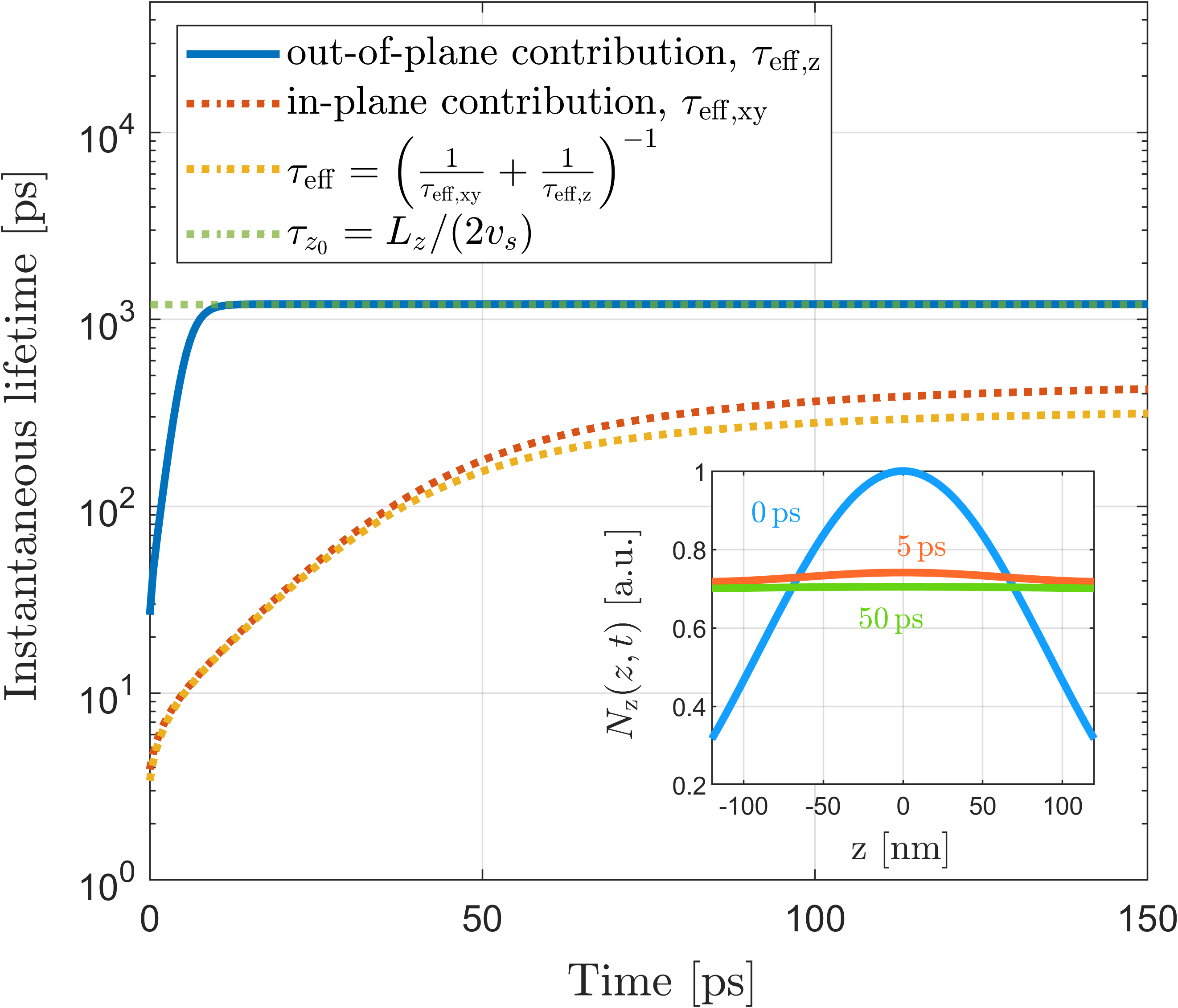
The time dependence of the instantaneous lifetimes is illustrated in Fig. 10. A surface recombination velocity of is considered. With increasing time, the out-of-plane lifetime (blue) tends to saturate much faster than the in-plane counterpart (red). The inset displays the out-of-plane carrier density distribution at zero time (light blue), (light red) and (light green) as a function of (see Sec. II in the Supplementary Material). The distribution is quickly smeared out, and the carrier decay rate, within a few picoseconds, is only limited by surface recombination. In contrast, the in-plane geometry, which is less trivial, tends to preserve the non-uniformity of the carrier distribution and retard the saturation of the in-plane instantaneous lifetime. The in-plane diffusion is also seen to be faster, and it dominates the total instantaneous lifetime (yellow) at any given time. This is generally the case unless the surface recombination is strong enough.
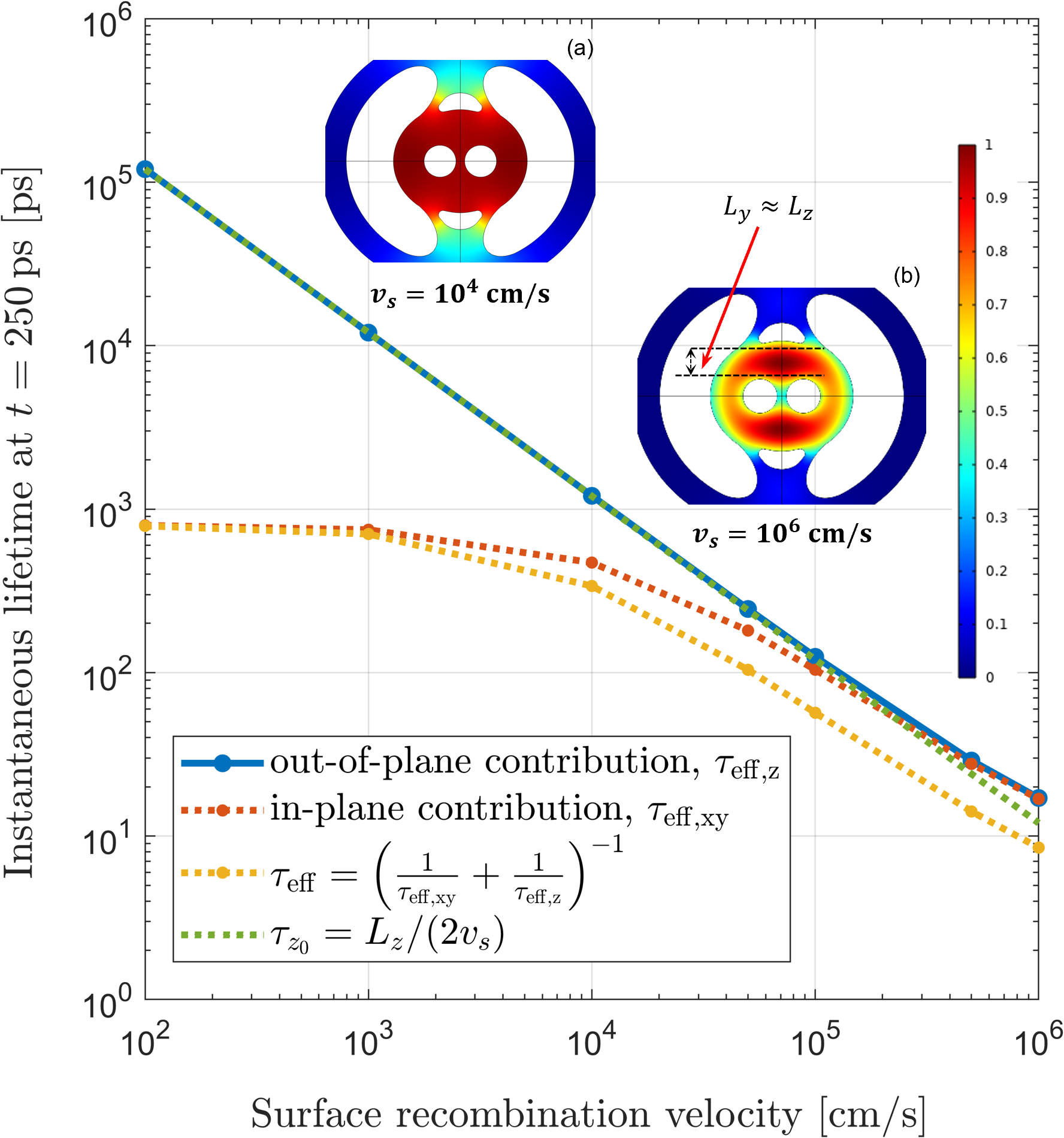
Fig. 11 illustrates the impact of surface recombination on the long timescale, where the in-plane carrier decay rate is close to saturation. For sufficiently large values of surface recombination, the out-of-plane instantaneous lifetime (blue) approaches the in-plane lifetime (red), with a nonnegligible impact on the total lifetime (yellow). The single-lifetime approximation (green) accurately captures the out-of-plane lifetime unless the surface recombination is high. The insets display the in-plane carrier density distribution for (a) moderate and (b) high values of surface recombination. Interestingly, large values of surface recombination tend to split the carriers and trap them in the space between the bowtie holes and the air openings above and below. The size along the -direction, , of this interstitial space (see inset b) roughly corresponds to the cavity thickness, , explaining why the out-of-plane and in-plane lifetimes tend to coincide. We have noticed similar trapping phenomena in the other photonic cavities (not shown). The observation suggests that the in-plane diffusion may be described as a one-dimensional phenomenon at sufficiently long times and high enough values of surface recombination. However, we expect the effective diffusion length to depend on the specific in-plane geometry, which prevents further general considerations.
If the out-of-plane excitation profile is not symmetric with respect to or the surface recombination velocity is not the same at the top and bottom surface of the cavity, the out-of-plane diffusion is generally asymmetric. In this case, the values of governing the diffusion lifetimes (cf. Eq. 35) are determined by
| (43) |
with and being the surface recombination velocity at the top and bottom surface of the cavity, respectively. The expression of (cf. Eq. 38) is also generalized (see Sec. III in the Supplementary Material), and takes into account that the eigenmodes are not even functions of . In practice, the out-of-plane diffusion is asymmetric if the substrate and cladding materials below and above the cavity, respectively, are different (with thus being asymmetric), or in general if the top and bottom surface feature different defect densities.
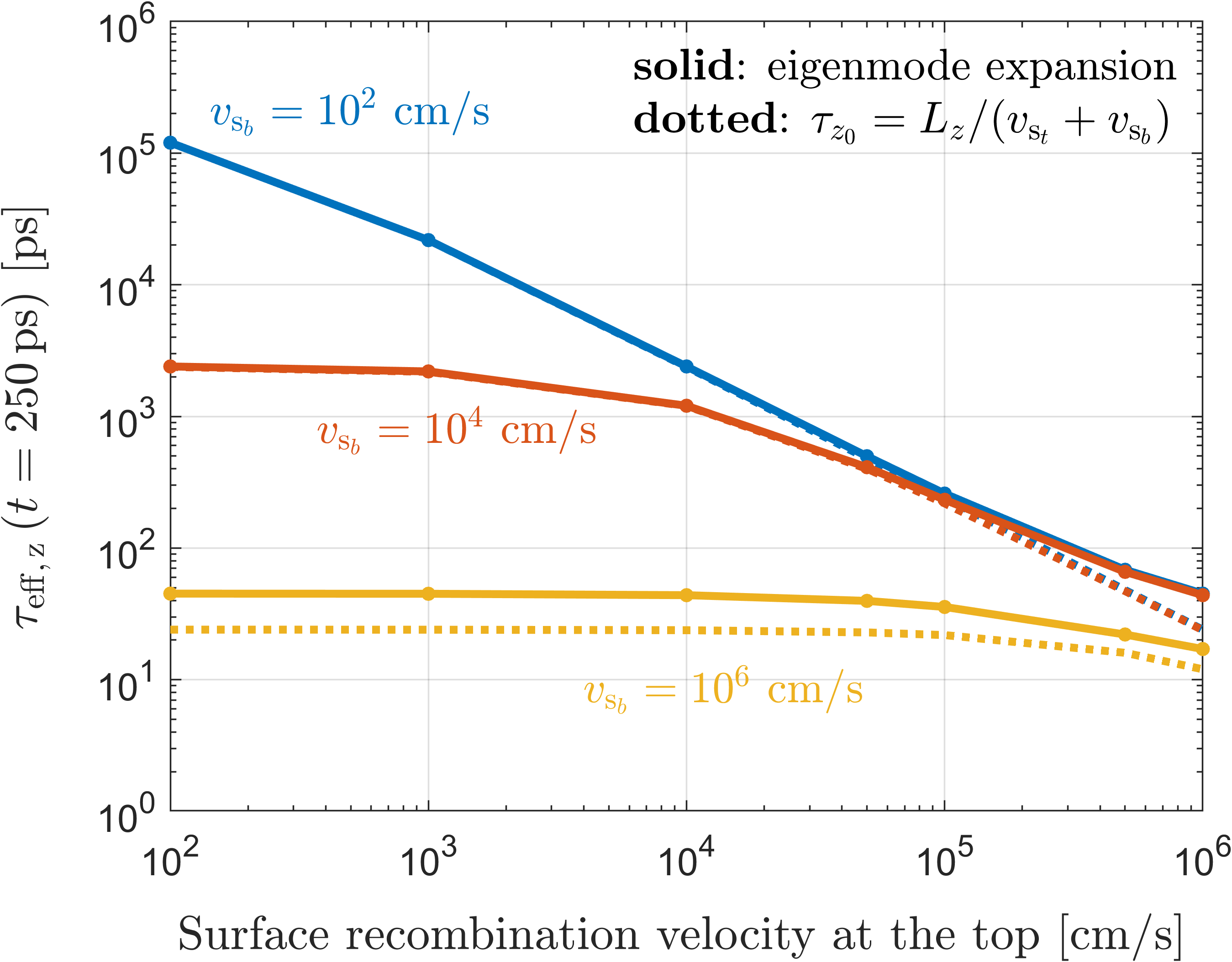
For example, we consider again the EDC ring cavity in Tab. 1. The cavity remains -symmetric (with thus being unchanged), but and are now allowed to differ. We focus on the long timescale, where the impact of surface recombination is significant, and the contribution of the out-of-plane diffusion to the total instantaneous lifetime may be nonnegligible. Fig. 12 shows the out-of-plane instantaneous lifetime at (solid) versus the surface recombination velocity at the top surface of the cavity. We also include the single-lifetime approximation (dotted, Eq. 40) with the surface recombination, , replaced by the average value of and . For low (blue) and moderate values (red) of , the out-of-plane instantaneous lifetime as obtained from the eigenmode expansion only differs from the single-lifetime approximation at sufficiently high values of . In contrast, large surface recombination values (yellow) at either the top or bottom surface degrade the accuracy of the single-lifetime approximation, irrespective of the surface recombination velocity at the other surface.
VI Conclusions
In conclusion, we have investigated the diffusion of carriers in semiconductor nanoscale resonators by employing an efficient eigenmode expansion technique. The response function of the mode-averaged (or effective) carrier density is found from the eigenmodes of the ambipolar diffusion equation, at variance with time-domain simulations of previous works Moille et al. (2016b). Importantly, we have shown that emerging dielectric cavities with extreme dielectric confinement (EDC) Hu and Weiss (2016); Choi et al. (2017); Wang et al. (2018); Albrechtsen et al. (2022) reduce the time it takes for the carriers to diffuse out of the effective mode area of interest. This is due to the tight confinement of the electric field to a hot spot. Thus, the effective carrier density decay rate is accelerated, which is promising for optical switching applications compared to more conventional geometries.
The eigenmode approach singles out the contribution to the effective carrier density decay rate due to the in-plane and out-of-plane cavity geometry. The in-plane contribution is found to dominate unless the surface recombination is high and the timescale of interest is sufficiently long. Furthermore, we have quantified the instantaneous decay rate of the effective carrier density, as a function of time and surface recombination, and compared EDC geometries with conventional photonic crystal designs. In contrast, previous works often rely on multi-exponential fits of nonlinear switching experiments Heuck et al. (2013); Bazin et al. (2014a), where the impact of carrier diffusion is difficult to isolate.
The eigenmode approach captures the long-timescale decay rate with only a few eigenmodes, making the method advantageous compared to time-domain simulations. Moreover, sorting the eigenmodes by their excitation coefficients significantly improves the method convergence speed on the short timescale. Future works may conveniently exploit the formulation herein illustrated (in short, Eq. 28, Eq. 39 and Eq. 42) to systematically optimize the carrier decay rate at given times, e.g., by inverse design Jensen and Sigmund (2011); Molesky et al. (2018).
References
- Chai et al. (2017) Z. Chai, X. Hu, F. Wang, X. Niu, J. Xie, and Q. Gong, Advanced Optical Materials 5, 1600665 (2017).
- Taghinejad and Cai (2019) M. Taghinejad and W. Cai, ACS Photonics 6, 1082 (2019).
- Ono et al. (2020) M. Ono, M. Hata, M. Tsunekawa, K. Nozaki, H. Sumikura, H. Chiba, and M. Notomi, Nature Photonics 14, 37 (2020).
- Guo et al. (2022) Q. Guo, R. Sekine, L. Ledezma, R. Nehra, D. J. Dean, A. Roy, R. M. Gray, S. Jahani, and A. Marandi, Nature Photonics 16, 625 (2022).
- Husko et al. (2009) C. Husko, A. De Rossi, S. Combrié, Q. V. Tran, F. Raineri, and C. W. Wong, Applied Physics Letters 94, 021111 (2009).
- Nozaki et al. (2010) K. Nozaki, T. Tanabe, A. Shinya, S. Matsuo, T. Sato, H. Taniyama, and M. Notomi, Nature Photonics 4, 477 (2010).
- Yu et al. (2013) Y. Yu, E. Palushani, M. Heuck, N. Kuznetsova, P. T. Kristensen, S. Ek, D. Vukovic, C. Peucheret, L. K. Oxenløwe, S. Combrié, A. de Rossi, K. Yvind, and J. Mørk, Opt. Express 21, 31047 (2013).
- Bazin et al. (2014a) A. Bazin, K. Lenglé, M. Gay, P. Monnier, L. Bramerie, R. Braive, G. Beaudoin, I. Sagnes, R. Raj, and F. Raineri, Applied Physics Letters 104, 011102 (2014a).
- Moille et al. (2016a) G. Moille, S. Combrié, L. Morgenroth, G. Lehoucq, F. Neuilly, B. Hu, D. Decoster, and A. de Rossi, Laser & Photonics Reviews 10, 409 (2016a).
- Colman et al. (2016) P. Colman, P. Lunnemann, Y. Yu, and J. Mørk, Phys. Rev. Lett. 117, 233901 (2016).
- Saudan et al. (2022) Q. Saudan, D. A. Bekele, G. Dong, Y. Yu, K. Yvind, J. Mørk, and M. Galili, Opt. Express 30, 7457 (2022).
- Kountouris et al. (2022) G. Kountouris, J. Mørk, E. V. Denning, and P. T. Kristensen, Opt. Express 30, 40367 (2022).
- Bazin et al. (2014b) A. Bazin, R. Raj, and F. Raineri, J. Lightwave Technol. 32, 952 (2014b).
- Bekele et al. (2019) D. Bekele, Y. Yu, K. Yvind, and J. Mork, Laser & Photonics Reviews 13, 1900054 (2019).
- Moille et al. (2016b) G. Moille, S. Combrié, and A. De Rossi, Phys. Rev. A 94, 023814 (2016b).
- Saldutti et al. (2021) M. Saldutti, M. Xiong, E. Dimopoulos, Y. Yu, M. Gioannini, and J. Mørk, Nanomaterials 11 (2021), 10.3390/nano11113030.
- Hu and Weiss (2016) S. Hu and S. M. Weiss, ACS Photonics 3, 1647 (2016).
- Choi et al. (2017) H. Choi, M. Heuck, and D. Englund, Phys. Rev. Lett. 118, 223605 (2017).
- Wang et al. (2018) F. Wang, R. E. Christiansen, Y. Yu, J. Mørk, and O. Sigmund, Applied Physics Letters 113, 241101 (2018).
- Albrechtsen et al. (2022) M. Albrechtsen, B. Vosoughi Lahijani, R. E. Christiansen, V. T. H. Nguyen, L. N. Casses, S. E. Hansen, N. Stenger, O. Sigmund, H. Jansen, J. Mørk, and S. Stobbe, Nature Communications 13, 6281 (2022).
- Johnson et al. (2006) T. J. Johnson, M. Borselli, and O. Painter, Opt. Express 14, 817 (2006).
- Heuck et al. (2013) M. Heuck, S. Combrié, G. Lehoucq, S. Malaguti, G. Bellanca, S. Trillo, P. T. Kristensen, J. Mørk, J. P. Reithmaier, and A. de Rossi, Applied Physics Letters 103, 181120 (2013).
- Tanabe et al. (2008) T. Tanabe, H. Taniyama, and M. Notomi, J. Lightwave Technol. 26, 1396 (2008).
- Schuller et al. (2010) J. A. Schuller, E. S. Barnard, W. Cai, Y. C. Jun, J. S. White, and M. L. Brongersma, Nature Materials 9, 193 (2010).
- Wang and Shen (2006) F. Wang and Y. R. Shen, Phys. Rev. Lett. 97, 206806 (2006).
- Khurgin (2015) J. B. Khurgin, Nature Nanotechnology 10, 2 (2015).
- Jensen and Sigmund (2011) J. Jensen and O. Sigmund, Laser & Photonics Reviews 5, 308 (2011).
- Molesky et al. (2018) S. Molesky, Z. Lin, A. Y. Piggott, W. Jin, J. Vucković, and A. W. Rodriguez, Nature Photonics 12, 659 (2018).
- Sze and Ng (2006) S. M. Sze and K. K. Ng, Physics of semiconductor devices, 3rd ed. (John Wiley & Sons, Inc., 2006).
- Liu (2005) J.-M. Liu, Photonic devices (Cambridge University Press, 2005).
- Nelson (2003) J. Nelson, The physics of solar cells (Imperial College Press, 2003).
- Tessler and Eistenstein (1993) N. Tessler and G. Eistenstein, IEEE Journal of Quantum Electronics 29, 1586 (1993).
- Gready and Eisenstein (2013) D. Gready and G. Eisenstein, IEEE Journal of Selected Topics in Quantum Electronics 19, 1900307 (2013).
- Tibaldi et al. (2019) A. Tibaldi, F. Bertazzi, M. Goano, R. Michalzik, and P. Debernardi, IEEE Journal of Selected Topics in Quantum Electronics 25, 1 (2019).
- Saldutti et al. (2020) M. Saldutti, A. Tibaldi, F. Cappelluti, and M. Gioannini, Photon. Res. 8, 1388 (2020).
- Vasileska et al. (2010) D. Vasileska, S. M. Goodnick, and G. Klimeck, Computational Electronics: Semiclassical and Quantum Device Modeling and Simulation (CRC Press, 2010).
- Mark and Mørk (1992) J. Mark and J. Mørk, Applied Physics Letters 61, 2281 (1992).
- Borghi et al. (2021) M. Borghi, D. Bazzanella, M. Mancinelli, and L. Pavesi, Opt. Express 29, 4363 (2021).
- Moille et al. (2017) G. Moille, S. Combrié, K. Fuchs, M. Yacob, J. P. Reithmaier, and A. de Rossi, Opt. Lett. 42, 795 (2017).
- Shockley and Read (1952) W. Shockley and W. T. Read, Phys. Rev. 87, 835 (1952).
- Hall (1952) R. N. Hall, Phys. Rev. 87, 387 (1952).
- Pierret (2002) R. F. Pierret, Advanced Semiconductor Fundamentals, 2nd ed. (Prentice Hall, 2002).
- Blakemore (1962) J. S. Blakemore, Semiconductor statistics (Pergamon Press, 1962).
- Aldaya et al. (2017) I. Aldaya, A. Gil-Molina, J. L. Pita, L. H. Gabrielli, H. L. Fragnito, and P. Dainese, Optica 4, 1219 (2017).
- Novarese et al. (2022) M. Novarese, S. R. Garcia, S. Cucco, D. Adams, J. Bovington, and M. Gioannini, Opt. Express 30, 14341 (2022).
- Ahrenkiel et al. (1991) R. K. Ahrenkiel, B. M. Keyes, and D. J. Dunlavy, Journal of Applied Physics 70, 225 (1991).
- McKelvey (1966) J. P. McKelvey, Solid State and Semiconductor Physics (Robert Kreiger Publ. Co., 1966).
- van Roosbroeck (1953) W. van Roosbroeck, Phys. Rev. 91, 282 (1953).
- Haynes and Shockley (1951) J. R. Haynes and W. Shockley, Phys. Rev. 81, 835 (1951).
- McKelvey (1956) J. P. McKelvey, Journal of Applied Physics 27, 341 (1956).
- Coldren et al. (2012) L. A. Coldren, S. W. Corzine, and M. Mašanović, Diode Lasers and Photonic Integrated Circuits, 2nd ed. (John Wiley & Sons, Inc., 2012).
- Levinshtein et al. (1998) M. Levinshtein, S. Rumyantsev, and M. Shur, Handbook Series on Semiconductor Parameters, Vol. 2 (World Scientific, 1998).
- Engl et al. (1983) W. Engl, H. Dirks, and B. Meinerzhagen, Proceedings of the IEEE 71, 10 (1983).
- Mui and Coldren (1995) D. S. L. Mui and L. A. Coldren, Journal of Applied Physics 78, 3208 (1995).
- Schenk (1998) A. Schenk, Advanced Physical Models for Silicon Device Simulation (Springer-Verlag Wien GmbH, 1998).
- Nolte (1990) D. Nolte, Solid-State Electronics 33, 295 (1990).
- Black et al. (2017) L. E. Black, A. Cavalli, M. A. Verheijen, J. E. M. Haverkort, E. P. A. M. Bakkers, and W. M. M. Kessels, Nano Letters 17, 6287 (2017).
- Higuera-Rodriguez et al. (2017) A. Higuera-Rodriguez, B. Romeira, S. Birindelli, L. E. Black, E. Smalbrugge, P. J. van Veldhoven, W. M. M. Kessels, M. K. Smit, and A. Fiore, Nano Letters 17, 2627 (2017).
- Aberle et al. (1992) A. G. Aberle, S. Glunz, and W. Warta, Journal of Applied Physics 71, 4422 (1992).
- Donchev et al. (2018) V. Donchev, S. Georgiev, I. Leontis, and A. G. Nassiopoulou, ACS Applied Energy Materials 1, 3693 (2018).
- Girisch et al. (1988) R. Girisch, R. Mertens, and R. De Keersmaecker, IEEE Transactions on Electron Devices 35, 203 (1988).
- McIntosh and Black (2014) K. R. McIntosh and L. E. Black, Journal of Applied Physics 116 (2014), 10.1063/1.4886595.
- Dimitropoulos et al. (2005) D. Dimitropoulos, R. Jhaveri, R. Claps, J. C. S. Woo, and B. Jalali, Applied Physics Letters 86 (2005), 10.1063/1.1866635.
- Bennett et al. (1990) B. Bennett, R. Soref, and J. Del Alamo, IEEE Journal of Quantum Electronics 26, 113 (1990).
- Kristensen et al. (2020) P. T. Kristensen, K. Herrmann, F. Intravaia, and K. Busch, Adv. Opt. Photon. 12, 612 (2020).
- Kristensen et al. (2015) P. T. Kristensen, R.-C. Ge, and S. Hughes, Phys. Rev. A 92, 053810 (2015).
- Muljarov and Langbein (2017) E. A. Muljarov and W. Langbein, Phys. Rev. A 96, 017801 (2017).
- Kristensen et al. (2017) P. T. Kristensen, R.-C. Ge, and S. Hughes, Phys. Rev. A 96, 017802 (2017).
- Barclay et al. (2005) P. E. Barclay, K. Srinivasan, and O. Painter, Opt. Express 13, 801 (2005).
- Saldutti et al. (2022) M. Saldutti, Y. Yu, P. T. Kristensen, G. Kountouris, and J. Mørk, in 2022 IEEE Photonics Conference (IPC) (2022) pp. 1–2.
- Xiong et al. (2023) M. Xiong, R. E. Christiansen, F. Schroeder, Y. Yu, L. N. Casses, E. Semenova, K. Yvind, N. Stenger, O. Sigmund, and J. Mørk, in 2023 Conference on Lasers and Electro-Optics Europe (CLEO Europe) (2023).
- Yu et al. (2014) Y. Yu, E. Palushani, M. Heuck, D. Vukovic, C. Peucheret, K. Yvind, and J. Mørk, Applied Physics Letters 105, 071112 (2014).
- Tanabe et al. (2007) T. Tanabe, K. Nishiguchi, A. Shinya, E. Kuramochi, H. Inokawa, M. Notomi, K. Yamada, T. Tsuchizawa, T. Watanabe, H. Fukuda, H. Shinojima, and S. Itabashi, Applied Physics Letters 90, 031115 (2007).