Charging-induced crafting of quantum-interfering nanospintronic paths across micronic MgO magnetic tunnel junctions
Paramagnetic carbon atoms in MgO magnetic tunnel junctions
Spin-polarized atom-level transport across a magnetic tunnel junction
Encoding information into the charge and spin state of a MgO magnetic tunnel junction’s paramagnetic atom
MgO spintronic device to encode information onto the charge and spin state of a paramagnetic atom
Encoding information onto the charge and spin state of a paramagnetic atom using MgO tunnelling spintronics
Abstract
An electrical current that flows across individual atoms or molecules can generate exotic quantum-based behavior, from memristive effects to Coulomb blockade and the promotion of quantum excited states. These fundamental effects typically appear one at a time in model junctions built using atomic tip or lateral techniques. So far, however, a viable industrial pathway for such discrete state devices has been lacking. Here, we demonstrate that a commercialized device platform can serve as this industrial pathway for quantum technologies. We have studied magnetic tunnel junctions with a MgO barrier containing C atoms. The paramagnetic localized electrons due to individual C atoms generate parallel nanotransport paths across the micronic deviceas deduced from magnetotransport experiments. Coulomb blockade effects linked to tunnelling magnetoresistance peaks can be electrically controlled, leading to a persistent memory effect. Our results position MgO tunneling spintronics as a promising platform to industrially implement quantum technologies.
Research on model atomic and molecular junctions has strongly progressed in the last two decades thanks to atomic tip and lateral junction building techniques. These technological advancements have helped reveal intriguing transport mechanisms, such as Coulomb blockade inside single-atom transistors [1], Coulomb drag and co-tunneling effects in capacitively coupled quantum dots [2], Franck-Condon blockade within carbon nanotubes [3], spin-phonon coupling in single-molecule magnets [4], Kondo effect with spin-oriented molecules [5], memristance and hysteresis linked to resistive switching [6, 7] and strong current fluctuations caused by vibrational coupling and structural changes [8]. More recently, quantum phenomena involving internal coherence and superposition have been reported, such as phonon interference [9], quantum interference and decoherence [10].
If ferromagnetic electrodes are used to establish a fixed spin referential, then the resulting spintronic device can better exploit the electron spin to encode quantum information [11] or harvest thermal energy using discrete spin states [12, 13]. While molecules offer elegant means of inserting discrete electronic states within a device, molecular spintronic strategies are still far from industrial deployment [14, 11].
Finally, much research has focused on transposing robust state changes to a junction’s spintronic response from more exotic barriers such as SrTiO3 [15] to the most widely developed industrial spintronic platform: the FeCoB/MgO/FeCoB magnetic tunnel junction (MTJ), with applications ranging from next-generation memories [16] and neuromorphic computing [17] to agile microwave emitters and artificial energy harvesting [18].
In this paper, we demonstrate several of the aforementioned quantum effects using the industrialization vector that is MgO tunnelling spintronics. Prior literature on MgO tunnelling indicates that structural defects can generate localized states within the tunnel barrier [19, 20, 21, 22, 23]. The tunnel barrier’s oxygen vacancies generate discrete electronic states that we have identified [23] and controlled [24] in our MgO junctions. These oxygen vacancies are diamagnetic. To achieve discrete, unpaired electron spin states, we introduce carbon atoms onto these oxygen vacancies [12] (see Methods).
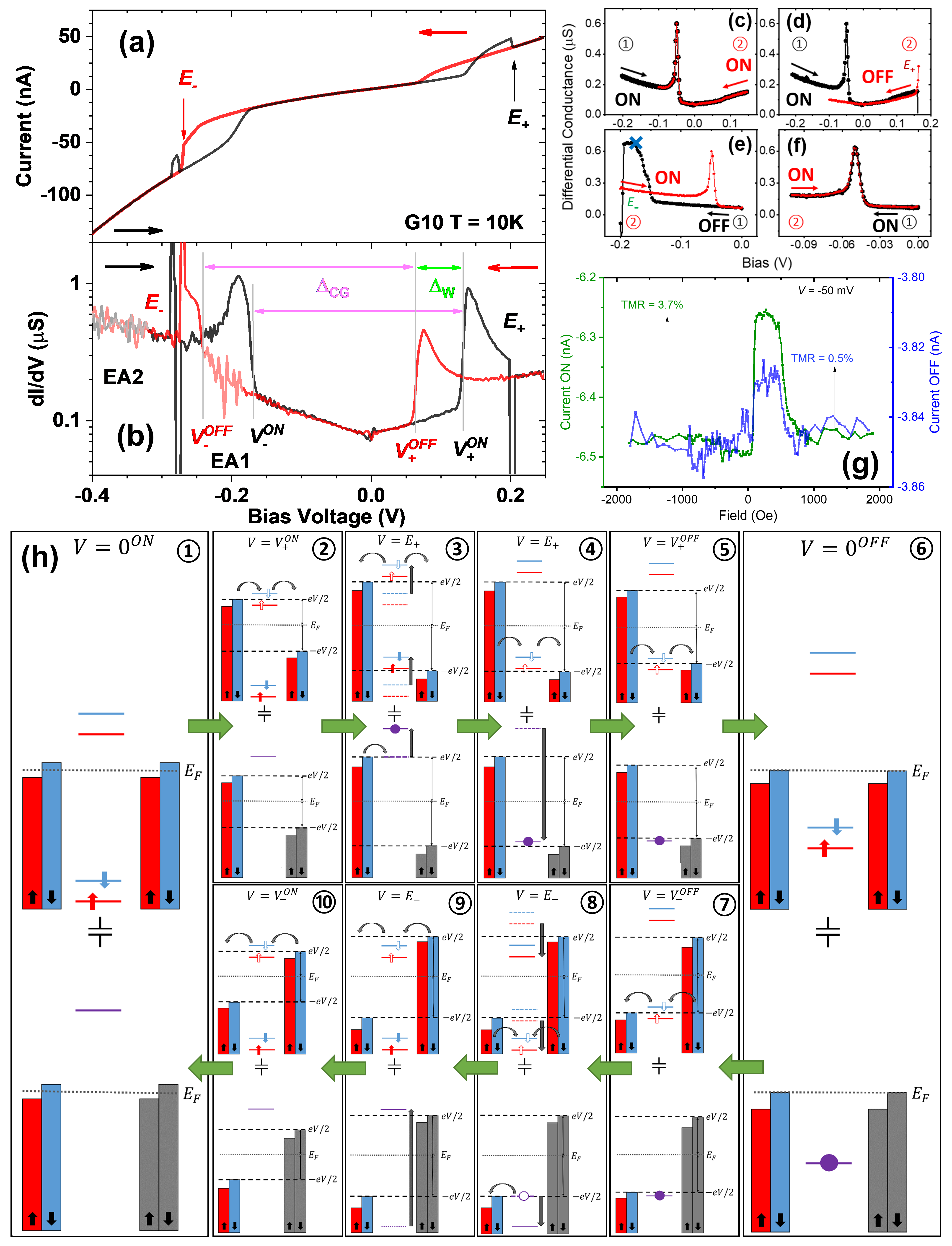
We observe that microscale MTJs with C atoms in the MgO barrier can exhibit noise and two/multi-level states of electrical transport (see Methods for technological processing). We now present evidence that the C-borne spin states can be electrically manipulated to encode information. The cyclical traces of junction G10 in Fig. 1(a) show two current branches that are linked through events and . Between these two events, the ON branch is represented in black while the OFF branch is in red. In Fig. 1(b) the corresponding set of differential conductance (d/d) is represented. We witness the presence of two conductance peaks at bias positions that depend on the direction of the voltage sweep. In the ON branch, they manifest around and , and they are shifted by 70 mV compared with the OFF branch. As discussed in SI Note 4, the constant voltage gap mV between the pair of conductance peaks can be tracked across several other states of the junction G10. Within this voltage gap, we observe an exponential increase in junction current. We therefore propose that these conductance peaks correspond to the edges of the Coulomb blockade regime across the MgO MTJ thanks to electronic states of C atoms in the MgO barrier. We also propose that the shift in the energy position of the Coulomb gap be the result of charging on ’environmental’ C atoms that do not participate in transport. This is supported in Fig. 1(a) by the presence of noisy regions EA1 and EA2 (semi-transparent datapoints). Indeed, the spectral position and width of these regions do not correspond to Coulomb blockade peaks in the present dataset, but rather in other datasets acquired on the same junction but with different ’transport’ and ’environmental’ attributions of the C atoms. See SI Note 4 for details.
To obtain atomic insight into the nanojunction’s nanotransport path, we use mV as a lower bound for the Coulomb gap of the ’transport’ quantum dot generated by the carbon atoms. Using an appropriate capacitance model, this allows us to estimate a 0.2 nm radius for the transport quantum dot (see SI Note 5), i.e. approximately one monolayer of MgO. This large Coulomb gap thus indicates that transport is proceeding across the electronic states of an individual carbon atom. Furthermore, if the voltage shift 70 mV between junction states corresponds to changing the environmental atom’s charge by 1 electron, then we infer that it is positioned at twice the radius away from the ’transport’ C atom (see SI Note 5).
The nanotransport path thus consists of at least one C atom, which is capacitively coupled to a nearby ’environmental’ C atom. Our survey of Coulomb blockade peaks (see SI Note 4) suggests that several C atoms can be in the transport path, and that a given atom may switch between ’transport’ and ’environmental’ roles depending on the atomic-level configuration of the nanotransport at each junction cooldown.
To prove that events and indeed code the shift of the Coulomb blockade peaks, we present in panels (c)-(f) of Fig. 1 the d/d traces from different paths in which we revert the voltage sweep direction just before and just after the events and . For each panel, the initial state of the junction is coded as ’1’, the color black and the arrow pointing towards the sweep direction. Once the sweep is inverted, the return state is presented in red and coded by the number 2. In panel (c), when in the ON state and starting at a low bias value, if the bias is increased so as to sweep through the Coulomb blockade peak (black data) but remain below the event, the return sweep (red data) reproduces the Coulomb blockade peak. In this scenario, if the event is reached, then the return trace shows no Coulomb blockade peak so the junction has switched to the OFF state and the peak encoding information has been erased (panel (d)). Similarly, when in the ON state and the branch 1 sweeps from above the Coulomb blockade peak without reaching the event, the peak readout is unchanged (panel (f)). Panel (e) however shows how, starting from the OFF state, reaching event causes the junction to revert to the ON state, characterized by the bit coded by the Coulomb blockade peak, which shows that the event indeed corresponds to the writing.
Given the low electric field amplitude and the ionic nature of MgO, an explanation of events and in terms of electromigration of oxygen vacancies is very unlikely [25]. Indeed, the ionic bonding of the MgO lattice makes it difficult for oxygen vacancies and other on-site defects to move within the crystal structure at room temperature and below [26]. Therefore, the observed resistive switching cannot be attributed to the migration of O2- ions as this is frequently the case in other oxides such as NiO [27]. It is possible, however, that an electromigration scenario be more favorable if the oxygen vacancies are filled [26] as is the case here.
Nevertheless, analogous hysteretic behavior induced by conductance jumps have been reported in molecular junctions [28, 29, 30] and scanning tunneling microscopy experiments [31, 32, 33, 34] but we now have showed that this phenomenon can also be observed in standard oxide-based junctions. The abrupt switching between two conductance branches results from a charging mechanism similar to the effect reported by Wu et al. [31]. Their results corroborate very well with our description featuring at least one control ’environmental’ atom, whose charge can be directly tuned by the voltage, which in return capacitively influences the energy landscape of the ’transport’ atom, as a gate voltage would control the current flow in single-electron transistors. In chemical words, the oxidation or reduction of the trapped C atom acting as the control quantum dot changes the nanotransport path taken by the electrons, which translates into different intensity branches.
We present in Fig. 1(h) the schematic of a two-atom model that can explain this memristive Coulomb blockage behavior. We consider two quantum dots: the upper one is the ’transport’ quantum dot (TQD) and is connected to both leads, while the lower one is ’environmental’ or ’control’ quantum dot (EQD) and is connected only to the left lead. Both quantum dots are capacitively coupled together.
Starting at in the OFF branch, the lower lying levels of the TDQ are filled, the upper lying are empty, and the single level of the EQD is empty (see Fig. 1(h)1). By increasing the voltage, a first conductance peak is seen on the d/d plot around which corresponds to the upper edge of the Coulomb blockade region. The potential of the left lead is approaching the upper level of the TDQ, allowing for the start of sequential tunneling (see Fig. 1(h)2). By increasing the voltage to , the potential of the left electrode aligns with the level of the EQD. A single electron can thus jump from the electrode to this level, which has the effect of lifting up the levels of both QDs in a first round. The upper lying levels of the TQD are now above the potential, while the lower levels rise between the potential window offered by the electrodes (see Fig. 1(h)3). During a second round, after equilibration, the electrons tunnel out of the TQD higher levels and sequential tunneling starts through the lower levels. The new dynamic filling of the energy levels of the TQD act capacitively in return on the EQD, which has the effect of lowering its level (see Fig. 1(h)4). Therefore, this capacitive back action traps the electron that filled the EQD level, preventing it from jumping back into the electrode. A conductance jump from the ON branch to the OFF branch is thus observed in this case and we can see that the potential will have to decrease to negative values in order to remove this trapped electron and revert back to the ON state.
From this unstable state in Fig. 1(h)3, the system can either go back to configuration 2 if the reverse jump process happens, or it can switch to the next transport regime if the filling of the transport atom changes because of this capacitive interaction. Hence, there is a small bias window in which the system can eventually fluctuate between two states before it stabilizes when the electron/dot on the environmental atom gets trapped as a result of a favorable capacitive coupling. The intensity of the fluctuation is driven by the ratio between the hopping frequencies of the environmental dot by the transport dot. If the jump frequency of the tunnelling processes on the TQD is much higher than that on the EQD, then the equilibration of the TQD will happen before any reverse jump can occur on the EQD, resulting in a single branch jump.
If the voltage is now decreased, another conductance peak is observed around which corresponds this time to the end of sequential tunneling through the lower lying level of the TQD (see Fig. 1(h)5). Going back to , the Coulomb blockade region is recovered but the levels of the TDQ are now arranged differently because of the presence of the electron in the EQD level (see Fig. 1(h)6). When the bias is decreased to negative values, sequential tunneling can start again through the lower levels of the TDQ around (see Fig. 1(h)7). Approaching , the potential of the left electrode now aligns again with the EQD level, allowing for the trapped electron to jump back into the lead. This change of charge borne by the EQD lowers the levels of QDs. Similarly, the upper levels are now located inside the potential window, while the lower levels are shifted below the potential of both electrodes, so they must be filled to reach equilibrium (see Fig. 1(h)8). This triggers a second round of effects where sequential tunneling now goes through the upper lying levels, while the lower lying levels stay filled. This change of electronic environment of the TQD acts again capacitively on the EQD, lifting up the energy level (see Fig. 1(h)9). The removing of the trapped electron thus triggers a branch jump from the OFF branch back to the ON branch. By increasing the potential, a final conductance peak is observed around which corresponds to the end of sequential tunneling through the upper lying level of the TQD (see Fig. 1(h)10). The cycle is completed at where the junction has indeed returned to the ON branch (see Fig. 1(h)1).
Close to , we notice that several branch jumps between the ON and OFF branches can occur. This behaviour is qualitatively expected by our schematics which can describe several jumps at this potential, resulting from multiple electron processes but the precise mechanisms that triggers these transitions remain to be detailed. We infer that at this special bias, the position of the energy levels is such that cotunneling phenomena mediated by phonons can trigger an avalanche of electrons which will momentarily fill the energy levels of the TQD, thereby lowering the level of the EQD, which would allow for an electron to fill it by tunneling from the left lead. This would make a jump back to the OFF branch momentarily possible, leading back to the situation in Fig. 1(h)8. The hysteretic nature of this phonon catalysis would allow for these multiple jumps only in the forward path but not during the reverse path. Indeed, according to polaron dynamics [35, 36], a population inversion between two phononic minima occurring around would change the interaction between the electrons and the phonons such that the phonons would favorably be in a higher potential well allowing for the reverse jump during the forward sweep, but they would be in the lower well during the reverse sweep, thus stabilizing the device in the OFF state. We point out that this hysteretic population change of the phonons could be linked to a structural rearrangement of the surroundings of the C atoms, notably in the angles of its bondings with the leads and the other species involved in transport [37, 34]. We also note that, depending on the position of the energy levels of the transport quantum dots relative to the environmental quantum dot, the events or may or may not occur around a conductance peak. A situation where the jump at occurs inside the Coulomb blockade region is presented in Fig. 1(d) and in SI Fig.S4. We described the situation of Fig. 1(b), but we can easily convince ourselves that if we place the upper levels of the TQD below the empty level of the EQD in the ON state, the potential of the left electrodes would address the level of the EQD around before reaching the edge of the Coulomb blockade region.
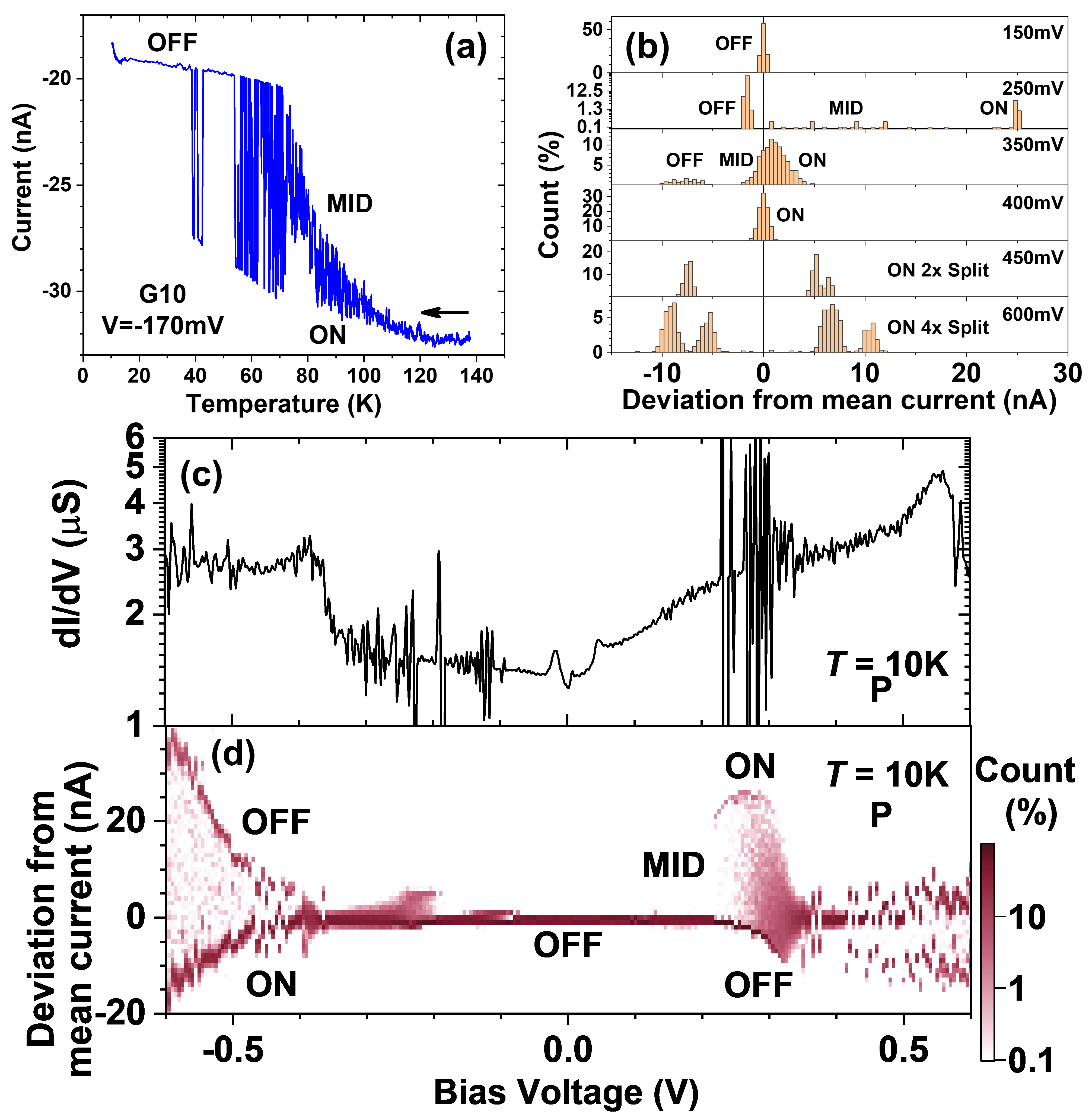
The discrete energy levels of the transport and environmental quantum dots give rise to quantum transport interference effects. We present in Fig. 2(a) the temperature dependence of the resistance measured on junction G10 at mV. As seen in Fig. 1(c), the junction is bistable at 10 K at this bias. Upon cooling down from 140K, the current broadens into two branches ON and OFF, with intermediate spectral weight of low intensity (MID branch). Further evidence of these regimes appears in SI Note 7. Since temperature alone can promote a dominant transport branch, we conclude that electron-phonon interactions, i.e. vibrons, also be involved in the quantum interference transport here, in line with prior literature [38, 39, 35, 40].
We use bias-dependent current statistics to observe transport branches due to quantum interference. We begin by plotting in Fig. 2(b) differential conductance data in the P magnetic state of junction C5 at K. On the log scale, we observe sizeable increases in conductance, and the clear appearance of noise for V and for V. Within (V) , after setting the dc applied bias, we measured the current 1000 times. The statistics of a given current deviation from the mean current as a function of applied bias are plotted in panel (c). Within V, the current remains essentially stable along the OFF branch. For V, the transition to the MID state can appear. This is especially visible within (V) . While the OFF branch shifts to values below the mean, the MID branch collapses into the dominant branch around V. A higher resolution map of this region is shown in SI Note 1. For V, this branch splits into two branches labelled ON and OFF. A similar branching is seen for V. Erratically, each of these two branches can split into two subbranches, for a total of four branches (see Fig. 2(d)). The noise in conductance thus arises from transport interference between these branches which are visualized by our current statistics.
Overall, these experimental findings support a picture of vibron-mediated co-tunnelling and/or Coulomb drag between nanotransport paths [2] due to blockade effects such as Franck-Condon blockade [38]. According to the theory of out-of-equilibrium polaron dynamics [35, 36], transport through an impurity with discrete energy levels such as a quantum dot or a molecular orbital which is strongly coupled to a vibrational degree of freedom and tunnel coupled to two leads explains the observed multi-stability of different states and the telegraphic switching between the different intensity branches. The voltage acts as an effective temperature and a force modulating the potential of the oscillator. Around specific voltage biases, the effective vibron energy potential landscape develops several minima, and thus promotes metastability between different occupation states. Two scenario are possible. 1) Thermally activated switching between different intensity branches related to each of the well separated potential minima can occur [7]. 2) Large fluctuations around a single intensity branch occur when at least two minima are close enough so that the quasi-degenerate states they encode trigger an interference effect [41, 42]. In this latter case, intermediate states outside the well minima are measured.
The memristive behavior of of the Coulomb blockade peak due to environmental charging represents one level of information encoding. Repeated testing indicates a write success rate of at least 81% (see SI Note 3). The MTJ’s two ferromagnetic leads enable us to examine how the spin polarization of the charge current impacts the atom-level memristive Coulomb blockade effect and quantum interference effects. To experimentally obtain spintronic contrast in our data, we examine the impact on transport of switching the orientation of electrode magnetization from parallel (P) to antiparallel (AP). The tunnel magnetoresistance TMR characterizes to what extent the two spin channels of current flowing across the device are asymmetric. Within the widely used Julliere model [43], this asymmetry arises from the spin-polarized densities of states of the ferromagnetic electrodes, and was extended to effectively encompass the filtering of electronic symmetries with majority spin polarization during solid-state tunnelling across MgO [44, 45].
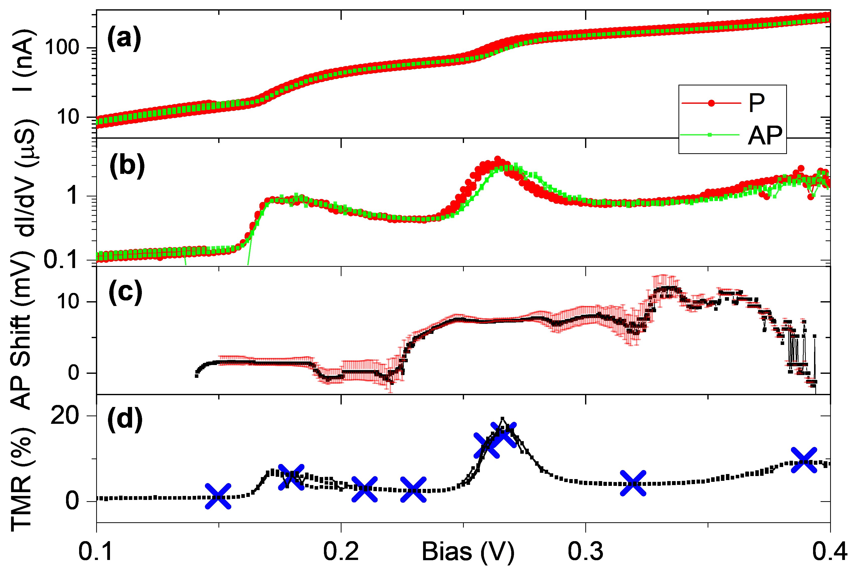
We plot in Fig. 3(a) the in the MTJ’s P and AP states at K. Both exhibit a series of plateaus and increases that are absent in junctions without C atoms[21, 22, 23]. The corresponding differential conductance (d/d) data (see panel (b)) reveals a series of peaks. While the P and AP datasets share similar traits, the AP plot appears to shift to higher bias as the onset of each conductance increase is reached. This is confirmed through an analysis of the correlated shift between the two datasets in Fig. 3(c) (see Methods).
In our MgO MTJs without C [21], we observe TMR % at 10 K around , and a mostly monotonous TMR decreasing with increasing . When C atoms are introduced into MgO, we observe only a few % TMR around . Instead, due to the shift in AP conductance to higher bias with each succeeding conductance peak, the TMR bias dependence closely mimicks the junction conductance (compare panels (c) and (d) of Fig. 3). This highly structured TMR bias dependence is confirmed through discrete datasets at fixed (crosses in Fig. 3(d)). We observe local TMR maxima precisely on the conductance peaks, with an absolute maximum of 15%.
To discuss the impact on spintronics of the memristive Coulomb blockade effect, we present data in Fig. 1(g) in both the ON and off state of the junction, taken at mV; i.e. precisely at the bias value corresponding to the memristive Coulomb blockade peak shown in panels (c-e) of Fig. 1. We observe that IP increases and that IP-IAP is multiplied by 7, so that the TMR increases from 0.5% in the OFF state to 3.7% in the ON state due to the Coulomb blockade peak. Within the paradigm of MgO tunnelling spintronics[46], this suggests that the Coulomb blockade peak effectively opens an additional transport channel with dominant majority spin carriers.
According to the theoretical work of Płomińska and Weymann [47], the similar set of bias-dependent conductance peaks in the MTJ’s P and AP states, leading to a similar TMR trace, is the signature of a special kind of Coulomb blockade effect named Pauli Spin blockade [48, 49, 50]. As the electronic level of the carbon transport atom is reached with applied bias, sequential tunneling is suppressed while co-tunnelling mechanisms become dominant and modify the spin state (and eventually the charge [12]) of the paramagnetic C atom, as a form of spintronic anisotropy [51, 52, 53]. With increasing voltage, the FeCoB/MgO tunnelling-induced accumulation of mostly spin up carriers lifts degeneracy of the spin states. This effectively lowers the spin up state relative to the spin down state. This spin splitting differs between the MTJ’s P and AP states due to different energy alignments of the C electronic levels [47, 12]. This effect is also modeled by our schematic in Fig 1(h) which features this spin splitting. Indeed, we witness that in the P state of the the electrodes presented in this figure, the potential of the electrodes will align with the split spin energy levels of the transport quantum dot at lower absolute bias than in the AP state, which would result in a voltage shift between the onsets of the conductance peaks leading to a positive TMR. SI Notes 1 and 4 provide additional evidence of this effect.
The conductance shift of Fig.3(c) is thus an experimental manifestation of spin accumulation. Spin accumulation also explains the shift in quantum interference data and the spin polarization of the transport branch therein (see SI Note 2). It also explains why the TMR bias dependence tracks that of junction conductance (see Fig. 3(d)), as well as the huge increase in IP-IAP due to the memristive Coulomb peak (see Fig. 1(g)) leading to the seven-fold TMR enhancement. The best agreement between the results of Płomińska and Weymann [47] and our experimental datasets is that of ’parallel’ or ’T-shaped’ electronic transport across spin states, rather than the other series scenario proposed. This supports the atomic description of the effective nanotransport path across our microscale MTJs.
To conclude, inserting C atoms into ultrathin MgO layers generates localized paramagnetic [12] states. Experiments on micronic FeCoB/MgO/FeCoB magnetic tunnel junctions, which are crafted using straightforward technological processes, show that the effective nanotransport path[22] involves individual C atoms. Their discrete energy levels promote Coulomb blockade effects that can be reproducibly shifted in energy by charging events on neighboring C atoms. The tunnel coupling between these transport and environmental carbon atoms promotes quantum interference effects. Spin-polarized transport induces spin accumulation that lifts the spin degeneracy of the unpaired C electron in MgO. This leads to a voltage shift in Coulomb peaks and quantum interference effects between the datasets in the MTJ’s P and AP magnetic states. Spin accumulation also accounts for the huge enhancement of the spintronic performance when a Coulomb peak is memristively controlled. We thus demonstrate how to use both the electron charge and spin to encode information on an individual paramagnetic atom in a solid-state, industrializable device. These results showcase MgO tunnelling spintronics as a promising industrial platform for quantum technologies at potentially practical temperatures, to deploy quantum transport effects that are normally only seen in model junctions. One track to achieve these effects at room temperature will be to engineer the impedances that electronically link the transport and environmental atoms to the magnetic tunnel junction electrodes. Final applications of quantum spintronics not only encompass information encoding [11], but also energy harvesting [12, 13] vectors.
Methods
Glass//Ta(5)/Co(10)/IrMn(7.5)/CoFeB(4)
/MgO(0.9)/C(0.6)MgO(1.7)/CoFeB(3)/Ta(2)/Pt(1) samples (all thicknesses in nm) were sputter-grown on Corning 1737 glass substrates [54]. Stacks were post-annealed in an in-plane magnetic field of 200 Oe for one hour at a temperature of 200 °C to magnetically pin the lower electrode thanks to the IrMn antiferromagnetic layer. Samples were then processed by optical lithography [55] into 20 m-diameter MTJs, and measured on a variable-temperature magnetotransport bench. 54 junctions were tested on these samples, 35 of them were either metallic of open circuit. Among the other 19 interesting junctions, all the reported effects have been observed in several of them. 8 of them presented memristive properties with branch jumps and conductance peaks, among which at least 3 presented magnetomemristive properties correlating with the conductance, while 7 of them presented jumps and noisy behaviors typical of interferences between several nanotransport paths (see SI Note 6).
Acknowledgements We gratefully acnkowledge PhD funding for M.L. from Ecole Polytechnique. We acknowledge financial support from the ANR (ANR-21-CE50-0039), the Contrat de Plan Etat-Region grants in 2006 and 2008, by “NanoTérahertz”, a project co-funded by the ERDF 2014–2020 in Alsace (European Union fund) and by the Region Grand Est through its FRCR call, by the impact project LUE-N4S part of the French PIA project “Lorraine Université d’Excellence”, reference ANR-15IDEX-04-LUE and by the FEDER-FSE “Lorraine et Massif Vosges 2014–2020”, a European Union Program. This work of the Interdisciplinary Thematic Institute QMat, as part of the ITI 2021-2028 program of the University of Strasbourg, CNRS and Inserm, was supported by IdEx Unistra (ANR 10 IDEX 0002), and by SFRI STRAT’US project (ANR 20 SFRI 0012) and EUR QMAT ANR-17-EURE-0024 under the framework of the French Investments for the Future Program.
References
- Ryndyk [2016] D. A. Ryndyk, “Electron-Electron Interaction and Coulomb Blockade,” in Theory of Quantum Transport at Nanoscale, Vol. 184 (Springer International Publishing, Cham, 2016) pp. 123–147.
- Keller et al. [2016] A. Keller, J. Lim, D. Sánchez, R. López, S. Amasha, J. Katine, H. Shtrikman, and D. Goldhaber-Gordon, “Cotunneling Drag Effect in Coulomb-Coupled Quantum Dots,” Physical Review Letters 117 (2016), 10.1103/PhysRevLett.117.066602.
- Burzurí et al. [2014] E. Burzurí, Y. Yamamoto, M. Warnock, X. Zhong, K. Park, A. Cornia, and H. S. J. van der Zant, “Franck–condon blockade in a single-molecule transistor,” 14, 3191–3196 (2014).
- Ganzhorn et al. [2013] M. Ganzhorn, S. Klyatskaya, M. Ruben, and W. Wernsdorfer, “Strong spin–phonon coupling between a single-molecule magnet and a carbon nanotube nanoelectromechanical system,” 8, 165–169 (2013).
- Parks et al. [2010] J. J. Parks, A. R. Champagne, T. A. Costi, W. W. Shum, A. N. Pasupathy, E. Neuscamman, S. Flores-Torres, P. S. Cornaglia, A. A. Aligia, C. A. Balseiro, G. K.-L. Chan, H. D. Abruña, and D. C. Ralph, “Mechanical control of spin states in spin-1 molecules and the underscreened kondo effect,” 328, 1370–1373 (2010).
- Miyamachi et al. [2012] T. Miyamachi, M. Gruber, V. Davesne, M. Bowen, S. Boukari, L. Joly, F. Scheurer, G. Rogez, T. K. Yamada, P. Ohresser, E. Beaurepaire, and W. Wulfhekel, “Robust spin crossover and memristance across a single molecule,” Nature Communications 3, 938 (2012).
- van der Molen and Liljeroth [2010] S. J. van der Molen and P. Liljeroth, “Charge transport through molecular switches,” 22, 133001 (2010).
- Secker et al. [2011] D. Secker, S. Wagner, S. Ballmann, R. Härtle, M. Thoss, and H. B. Weber, “Resonant Vibrations, Peak Broadening, and Noise in Single Molecule Contacts: The Nature of the First Conductance Peak,” Physical Review Letters 106 (2011), 10.1103/PhysRevLett.106.136807.
- Zeng et al. [2020] Y.-J. Zeng, D. Wu, X.-H. Cao, Y.-X. Feng, L.-M. Tang, and K.-Q. Chen, “Significantly enhanced thermoelectric performance of molecular junctions by the twist angle dependent phonon interference effect,” 8, 11884–11891 (2020).
- Greenwald et al. [2020] J. E. Greenwald, J. Cameron, N. J. Findlay, T. Fu, S. Gunasekaran, P. J. Skabara, and L. Venkataraman, “Highly nonlinear transport across single-molecule junctions via destructive quantum interference,” 16, 313–317 (2020).
- Katcko et al. [2021] K. Katcko, E. Urbain, F. Ngassam, L. Kandpal, B. Chowrira, F. Schleicher, U. Halisdemir, D. Wang, T. Scherer, D. Mertz, B. Leconte, N. Beyer, D. Spor, P. Panissod, A. Boulard, J. Arabski, C. Kieber, E. Sternitzky, V. Da Costa, M. Hehn, F. Montaigne, A. Bahouka, W. Weber, E. Beaurepaire, C. Kübel, D. Lacour, M. Alouani, S. Boukari, and M. Bowen, “Encoding Information on the Excited State of a Molecular Spin Chain,” Advanced Functional Materials 31, 2009467 (2021).
- Katcko et al. [2019] K. Katcko, E. Urbain, B. Taudul, F. Schleicher, J. Arabski, E. Beaurepaire, B. Vileno, D. Spor, W. Weber, D. Lacour, S. Boukari, M. Hehn, M. Alouani, J. Fransson, and M. Bowen, “Spin-driven electrical power generation at room temperature,” Communications Physics 2 (2019), 10.1038/s42005-019-0207-8.
- Chowrira et al. [2020] B. Chowrira, L. Kandpal, D. Mertz, C. Kieber, A. Bahouka, R. Bernard, L. Joly, E. Monteblanco, S. Mohapatra, H. P. Garcia, S. Elidrissi, M. Gavara, E. Sternitzky, V. D. Costa, M. Hehn, F. Montaigne, B. Vileno, F. Choueikani, P. Ohresser, D. Lacour, W. Weber, S. Boukari, and M. Bowen, “need to update,” (2020), arXiv:2009.10413 [cond-mat.mes-hall] .
- Barraud et al. [2016] C. Barraud, K. Bouzehouane, C. Deranlot, D. J. Kim, R. Rakshit, S. Shi, J. Arabski, M. Bowen, E. Beaurepaire, S. Boukari, F. Petroff, P. Seneor, and R. Mattana, “Phthalocyanine based molecular spintronic devices,” Dalton Transactions 45, 16694–16699 (2016).
- Bowen et al. [2006] M. Bowen, J.-L. Maurice, A. Barthélémy, P. Prod’homme, E. Jacquet, J.-P. Contour, D. Imhoff, and C. Colliex, “Bias-crafted magnetic tunnel junctions with bistable spin-dependent states,” Applied Physics Letters 89, 103517 (2006).
- Kent and Worledge [2015] A. D. Kent and D. C. Worledge, “A new spin on magnetic memories,” Nature Nanotechnology 10, 187–191 (2015).
- Torrejon et al. [2017] J. Torrejon, M. Riou, F. A. Araujo, S. Tsunegi, G. Khalsa, D. Querlioz, P. Bortolotti, V. Cros, K. Yakushiji, A. Fukushima, H. Kubota, S. Yuasa, M. D. Stiles, and J. Grollier, “Neuromorphic computing with nanoscale spintronic oscillators,” Nature 547, 428–431 (2017).
- Zhang et al. [2018] L. Zhang, B. Fang, J. Cai, M. Carpentieri, V. Puliafito, F. Garescì, P. K. Amiri, G. Finocchio, and Z. Zeng, “Ultrahigh detection sensitivity exceeding 10 V/W in spin-torque diode,” Applied Physics Letters 113, 102401 (2018).
- Freitas et al. [2007] P. P. Freitas, R. Ferreira, S. Cardoso, and F. Cardoso, “Magnetoresistive sensors,” Journal of Physics-Condensed Matter 19 (2007), 10.1088/0953-8984/19/16/165221.
- Lu et al. [2009] Y. Lu, M. Tran, H. Jaffrès, P. Seneor, C. Deranlot, F. Petroff, J.-M. George, B. Lépine, S. Ababou, and G. Jézéquel, “Spin-Polarized Inelastic Tunneling through Insulating Barriers,” Physical Review Letters 102, 176801 (2009).
- Schleicher et al. [2014] F. Schleicher, U. Halisdemir, D. Lacour, M. Gallart, S. Boukari, G. Schmerber, V. Davesne, P. Panissod, D. Halley, H. Majjad, Y. Henry, B. Leconte, A. Boulard, D. Spor, N. Beyer, C. Kieber, E. Sternitzky, O. Cregut, M. Ziegler, F. Montaigne, E. Beaurepaire, P. Gilliot, M. Hehn, and M. Bowen, “Localized states in advanced dielectrics from the vantage of spin- and symmetry-polarized tunnelling across MgO,” Nature Communications 5 (2014), 10.1038/ncomms5547.
- Studniarek et al. [2017] M. Studniarek, U. Halisdemir, F. Schleicher, B. Taudul, E. Urbain, S. Boukari, M. Hervé, C.-H. Lambert, A. Hamadeh, S. Petit-Watelot, O. Zill, D. Lacour, L. Joly, F. Scheurer, G. Schmerber, V. D. Costa, A. Dixit, P. A. Guitard, M. Acosta, F. Leduc, F. Choueikani, E. Otero, W. Wulfhekel, F. Montaigne, E. N. Monteblanco, J. Arabski, P. Ohresser, E. Beaurepaire, W. Weber, M. Alouani, M. Hehn, and M. Bowen, “Probing a device's active atoms,” Advanced Materials 29, 1606578 (2017).
- Schleicher et al. [2019] F. Schleicher, B. Taudul, U. Halisdemir, K. Katcko, E. Monteblanco, D. Lacour, S. Boukari, F. Montaigne, E. Urbain, L. M. Kandpal, J. Arabski, W. Weber, E. Beaurepaire, M. Hehn, M. Alouani, and M. Bowen, “Consolidated picture of tunnelling spintronics across oxygen vacancy states in MgO,” Journal of Physics D: Applied Physics 52, 305302 (2019).
- Taudul et al. [2017] B. Taudul, E. N. Monteblanco, U. Halisdemir, D. Lacour, F. Schleicher, F. Montaigne, E. Beaurepaire, S. Boukari, M. Hehn, M. Alouani, and M. Bowen, “Tunneling Spintronics across MgO Driven by Double Oxygen Vacancies,” Advanced Electronic Materials 3, 1600390 (2017).
- Bertin et al. [2011] E. Bertin, D. Halley, Y. Henry, N. Najjari, H. Majjad, M. Bowen, V. DaCosta, J. Arabski, and B. Doudin, “Random barrier double-well model for resistive switching in tunnel barriers,” Journal of Applied Physics 109, 083712 (2011).
- Aguiar-Hualde and Alouani [2014] J. M. Aguiar-Hualde and M. Alouani, “Taming the resistive switching in Fe/MgO/V/Fe magnetic tunnel junctions: An ab initio study,” Journal of Magnetism and Magnetic Materials 372, 167–172 (2014).
- Hwang et al. [2010] I. Hwang, M.-J. Lee, G.-H. Buh, J. Bae, J. Choi, J.-S. Kim, S. Hong, Y. S. Kim, I.-S. Byun, S.-W. Lee, S.-E. Ahn, B. S. Kang, S.-O. Kang, and B. H. Park, “Resistive switching transition induced by a voltage pulse in a Pt/NiO/Pt structure,” Applied Physics Letters 97, 052106 (2010).
- Jia et al. [2016] C. Jia, A. Migliore, N. Xin, S. Huang, J. Wang, Q. Yang, S. Wang, H. Chen, D. Wang, B. Feng, Z. Liu, G. Zhang, D.-H. Qu, H. Tian, M. A. Ratner, H. Q. Xu, A. Nitzan, and X. Guo, “Covalently bonded single-molecule junctions with stable and reversible photoswitched conductivity,” Science 352, 1443–1445 (2016).
- Lörtscher et al. [2006] E. Lörtscher, J. Ciszek, J. Tour, and H. Riel, “Reversible and controllable switching of a single-molecule junction,” 2, 973–977 (2006).
- Schwarz et al. [2016] F. Schwarz, G. Kastlunger, F. Lissel, C. Egler-Lucas, S. N. Semenov, K. Venkatesan, H. Berke, R. Stadler, and E. Lörtscher, “Field-induced conductance switching by charge-state alternation in organometallic single-molecule junctions,” Nature Nanotechnology 11, 170–176 (2016).
- Wu et al. [2008] S. W. Wu, N. Ogawa, G. V. Nazin, and W. Ho, “Conductance Hysteresis and Switching in a Single-Molecule Junction,” The Journal of Physical Chemistry C 112, 5241–5244 (2008).
- Leoni et al. [2011] T. Leoni, O. Guillermet, H. Walch, V. Langlais, A. Scheuermann, J. Bonvoisin, and S. Gauthier, “Controlling the Charge State of a Single Redox Molecular Switch,” Physical Review Letters 106 (2011), 10.1103/PhysRevLett.106.216103.
- Gerhard et al. [2017] L. Gerhard, K. Edelmann, J. Homberg, M. Valášek, S. G. Bahoosh, M. Lukas, F. Pauly, M. Mayor, and W. Wulfhekel, “An electrically actuated molecular toggle switch,” Nature Communications 8, 14672 (2017).
- Zhang et al. [2020] L. Zhang, T. Yang, W. Zhang, D. Qi, X. He, K. Xing, P. K. J. Wong, Y. P. Feng, and A. T. S. Wee, “Bi-stable electronic states of cobalt phthalocyanine molecules on two-dimensional vanadium diselenide,” Applied Materials Today 18, 100535 (2020).
- Mozyrsky, Hastings, and Martin [2006] D. Mozyrsky, M. B. Hastings, and I. Martin, “Intermittent polaron dynamics: Born-Oppenheimer approximation out of equilibrium,” Physical Review B 73 (2006), 10.1103/PhysRevB.73.035104.
- Galperin, Ratner, and Nitzan [2005] M. Galperin, M. A. Ratner, and A. Nitzan, “Hysteresis, Switching, and Negative Differential Resistance in Molecular Junctions: A Polaron Model,” Nano Letters 5, 125–130 (2005).
- Martínez-Blanco et al. [2015] J. Martínez-Blanco, C. Nacci, S. C. Erwin, K. Kanisawa, E. Locane, M. Thomas, F. von Oppen, P. W. Brouwer, and S. Fölsch, “Gating a single-molecule transistor with individual atoms,” Nature Physics 11, 640–644 (2015).
- Koch, von Oppen, and Andreev [2006] J. Koch, F. von Oppen, and A. V. Andreev, “Theory of the Franck-Condon blockade regime,” Physical Review B 74 (2006), 10.1103/PhysRevB.74.205438.
- Galperin, Ratner, and Nitzan [2007] M. Galperin, M. A. Ratner, and A. Nitzan, “Molecular transport junctions: vibrational effects,” Journal of Physics: Condensed Matter 19, 103201 (2007).
- Aradhya and Venkataraman [2013] S. V. Aradhya and L. Venkataraman, “Single-molecule junctions beyond electronic transport,” Nature Nanotechnology 8, 399–410 (2013).
- Wierzbicki and Swirkowicz [2011] M. Wierzbicki and R. Swirkowicz, “Influence of interference effects on thermoelectric properties of double quantum dots,” Physical Review B 84 (2011), 10.1103/PhysRevB.84.075410.
- Wu et al. [2004] S. W. Wu, G. V. Nazin, X. Chen, X. H. Qiu, and W. Ho, “Control of Relative Tunneling Rates in Single Molecule Bipolar Electron Transport,” Physical Review Letters 93 (2004), 10.1103/PhysRevLett.93.236802.
- Julliere [1975] M. Julliere, “Tunneling between ferromagnetic films,” Physics Letters A 54, 225–226 (1975).
- Bowen et al. [2001] M. Bowen, V. Cros, F. Petroff, A. Fert, C. Martinez Boubeta, J. L. Costa-Krämer, J. V. Anguita, A. Cebollada, F. Briones, J. M. de Teresa, L. Morellón, M. R. Ibarra, F. Güell, F. Peiró, and A. Cornet, “Large magnetoresistance in Fe/MgO/FeCo(001) epitaxial tunnel junctions on GaAs(001),” Applied Physics Letters 79, 1655–1657 (2001).
- Kozub, Galperin, and Vinokur [2018] V. Kozub, Y. Galperin, and V. Vinokur, “Coulomb blockade-tuned indirect exchange in ferromagnetic nanostructures,” Journal of Magnetism and Magnetic Materials 465, 304–308 (2018).
- Moodera, Miao, and Santos [2010] J. S. Moodera, G.-X. Miao, and T. S. Santos, “Frontiers in spin-polarized tunneling,” Physics Today 63, 46–51 (2010).
- Płomińska and Weymann [2019] A. Płomińska and I. Weymann, “Magnetoresistive properties of a double magnetic molecule spin valve in different geometrical arrangements,” Journal of Magnetism and Magnetic Materials 480, 11–21 (2019).
- Fransson and Råsander [2006] J. Fransson and M. Råsander, “Pauli spin blockade in weakly coupled double quantum dots,” Physical Review B 73 (2006), 10.1103/PhysRevB.73.205333.
- Kuo, Shiau, and Chang [2011] D. M.-T. Kuo, S.-Y. Shiau, and Y.-c. Chang, “Theory of spin blockade, charge ratchet effect, and thermoelectrical behavior in serially coupled quantum dot system,” Physical Review B 84 (2011), 10.1103/PhysRevB.84.245303.
- Płomińska and Weymann [2016] A. Płomińska and I. Weymann, “Pauli spin blockade in double molecular magnets,” Physical Review B 94 (2016), 10.1103/PhysRevB.94.035422.
- Misiorny, Weymann, and Barnaś [2009] M. Misiorny, I. Weymann, and J. Barnaś, “Spin effects in transport through single-molecule magnets in the sequential and cotunneling regimes,” Physical Review B 79, 224420 (2009).
- Misiorny and Weymann [2014] M. Misiorny and I. Weymann, “Transverse anisotropy effects on spin-resolved transport through large-spin molecules,” Physical Review B 90 (2014), 10.1103/PhysRevB.90.235409.
- Saygun et al. [2016] T. Saygun, J. Bylin, H. Hammar, and J. Fransson, “Voltage-Induced Switching Dynamics of a Coupled Spin Pair in a Molecular Junction,” Nano Letters 16, 2824–2829 (2016).
- Bernos et al. [2010] J. Bernos, M. Hehn, F. Montaigne, C. Tiusan, D. Lacour, M. Alnot, B. Negulescu, G. Lengaigne, E. Snoeck, and F. G. Aliev, “Impact of electron-electron interactions induced by disorder at interfaces on spin-dependent tunneling in Co-Fe-B/MgO/Co-Fe-B magnetic tunnel junctions,” Physical Review B 82 (2010), 10.1103/PhysRevB.82.060405.
- Halley et al. [2008] D. Halley, H. Majjad, M. Bowen, N. Najjari, Y. Henry, C. Ulhaq-Bouillet, W. Weber, G. Bertoni, J. Verbeeck, and G. Van Tendeloo, “Electrical switching in Fe/Cr/MgO/Fe magnetic tunnel junctions,” Applied Physics Letters 92, 212115 (2008).
![[Uncaptioned image]](/html/2308.16592/assets/x1.png)
![[Uncaptioned image]](/html/2308.16592/assets/x2.png)
![[Uncaptioned image]](/html/2308.16592/assets/x3.png)
![[Uncaptioned image]](/html/2308.16592/assets/x4.png)
![[Uncaptioned image]](/html/2308.16592/assets/x5.png)
![[Uncaptioned image]](/html/2308.16592/assets/x6.png)
![[Uncaptioned image]](/html/2308.16592/assets/x7.png)
![[Uncaptioned image]](/html/2308.16592/assets/x8.png)
![[Uncaptioned image]](/html/2308.16592/assets/x9.png)
![[Uncaptioned image]](/html/2308.16592/assets/x10.png)
![[Uncaptioned image]](/html/2308.16592/assets/x11.png)
![[Uncaptioned image]](/html/2308.16592/assets/x12.png)
![[Uncaptioned image]](/html/2308.16592/assets/x13.png)
![[Uncaptioned image]](/html/2308.16592/assets/x14.png)