Edge Magnetoplasmon Dispersion and Time-Resolved Plasmon Transport in a Quantum Anomalous Hall Insulator
Abstract
A quantum anomalous Hall (QAH) insulator breaks reciprocity by combining magnetic polarization and spin-orbit coupling to generate a unidirectional transmission of signals in the absence of an external magnetic field. Such behavior makes QAH materials a good platform for the innovation of circulator technologies. However, it remains elusive as to how the wavelength of the chiral edge plasmon relates to its frequency and how the plasmon wave packet is excited in the time domain in a QAH insulator. Here, we investigate the edge magnetoplasmon (EMP) resonances in Cr-(Bi,Sb)2Te3 by frequency and time domain measurements. From disk shaped samples with various dimensions, we obtain the dispersion relation of EMPs and extract the drift velocity of the chiral edge state. From the time-resolved transport measurements, we identify the velocity of the plasmon wave packet and observe a transition from the edge to bulk transport at an elevated temperature. We show that the frequency and time domain measurements are well modeled by loss from the microwave induced dissipative channels in the bulk area. Our results demonstrate that the EMP decay rate can be significantly reduced by applying a low microwave power and fabricating devices of larger diameter m. In a m sample, a non-reciprocity of 20 dB has been realized at 1.3 GHz, shining light on using QAH insulators to develop on-chip non-reciprocal devices.
I Introduction
Quantum Hall (QH) and quantum anomalous Hall (QAH) materials are promising candidates for construction of small footprint non-reciprocal microwave devices, owing to their ability to convert an electromagnetic wave into deep-subwavelength chiral magneto-plasmonic modes.[1, 2, 3, 4, 5] Recent experiments have demonstrated robust chiral magnetoplasmon excitations in QAH materials, paving the way to developing on-chip non-reciprocal components.[6] However, further progress is hindered by a lack of knowledge about the EMP dispersion,[7] which is critical for tuning the plasmon resonance to develop chip-level components for quantum processors, such as cryogenic circulators and isolators. Moreover, the time-domain dynamics of plasmon transport has not been studied in a QAH system. Understanding plasmon wave packet propagation over a wide temperature range will aid device development as well as material advancement.
In addition to potential quantum-classical interface applications, two-dimensional (2D) magnetoplasmons in a quantum Hall system, which exhibits gapped bulk states and gapless one-way edge states, are topologically analogous to a -wave topological superconductor around zero frequency.[8] Recent microwave experiments have revealed the existence of topologically protected magnetoplasmons in a 2D electron gas (2DEG) in the GHz frequency range.[9] As a result of the unique topological properties of 2D magnetoplasmons, magnetoplasmon zero modes have been predicted in graphene, [10, 11] 2DEG,[8] and QAH insulators. It is therefore of great interest from both a fundamental and a practical viewpoint to measure the dispersion relation of EMPs, identify their decay times, and understand how they dissipate in the presence of microwave radiation.
Here, we report the dispersion relation and the time-resolved plasmon transport in the QAH insulator, Cr-doped (Bi,Sb)2Te3. Three-port circulator structures were fabricated with a mesa radius ranging from 15 to 125 m. In the largest device, we find a 20 dB non-reciprocity for the low-frequency EMP resonance through microwave transmission measurements. In the smallest device, the non-reciprocity response still exists for the resonant frequency at 3.2 GHz, where the transverse width of EMPs is comparable to the mesa radius. Furthermore, the time-dependent measurement shows that in addition to the EMP, the bulk plasmon transport starts to appear when the temperature is increased above K. We estimated the plasmon decay time and discuss the associated dissipation mechanism.
II Results
II.1 Sample preparation
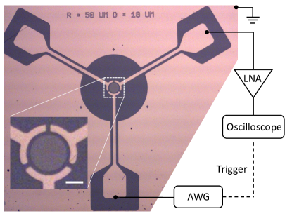
The Cr0.12(Bi0.26Sb0.62)2Te3 QAH samples with a film thickness of 6 quintuple layers (QL) were deposited using the Molecular Beam Epitaxy technique. Following the material growth, the circulator devices were patterned using a standard photo-lithography process. Peripheral co-planar waveguides made from Ti/Au 10/100 nm were deposited using an electron beam evaporator. In this work, we studied five devices with radii ranging from 15 to 125 m (Fig. 1). Device dimensions are listed in the Supplemental Material (SM).
II.2 Device characterization
Characterization of QH materials normally requires superconducting magnets with Tesla-level magnetic fields capabilities. [12] A unique feature of QAH materials is the ability to perform experiments without the need of superconducting magnets, typical off-the-shelf neodymium magnets with remnant fields on the order of tens of mT are sufficient to reach the quantized Hall state when cooling the device from room temperature. [13] This feature allows us to perform measurements in a dilution refrigerator housing multiple qubit systems without any added noise. Details of the experimental cryogenic setup can be found in Section II of the SM.
II.3 Microwave transmission measurements
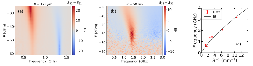
The frequency domain results for two selected samples are shown in Figs. 2 a and b. The quantity of interest is the non-reciprocity of the sample. In a perfectly reciprocal device, the non-reciprocity would be zero. The non-reciprocity is determined by the net difference in signal measured as , when performing -parameter measurements of the transmitted power on port 3 excited from port 2 () and port 1 (), respectively. For the m sample, we observe the first EMP resonant frequency near GHz, and the second harmonic near GHz. We observed that the non-reciprocity of the first mode broadens while its frequency shifts left towards lower frequencies. Similar behaviour is observed for the second mode, with the onset at much lower port powers. The frequency response for the m sample is shown in Fig. 2b. It exhibits one EMP mode near GHz, with an overall magnitude of the non-reciprocity less than that of the m sample.
In microwave transmission measurements, the narrow EMP resonances appear as a result of the QAH phase in which the longitudinal resistance is negligible and the Hall resistance becomes quantized. The EMP mode in the QAH regime is the resonant edge excitation of charge density with a wavelength determined by the sample perimeter viz. , (). is the perimeter of the QAH mesa, and is the radius of the mesa. The resonant frequency of the fundamental () and th harmonic modes can be estimated to occur in the range of GHz for typical mesa parameters . From the EMP mode resonant frequency there follows an estimate of the phase velocity given as . The dispersion relation for a general 2D system with sharp edge conductance can be modeled by[14, 15, 16]
| (1) |
where is the wave vector, the Hall conductivity, the Chern number, the effective dielectric constant, the drift velocity of the 1D edge state, and the physical width of the EMP mode at the edge.
From the microwave transmission measurements, we determined the EMP dispersion relation by plotting the dependence of the resonance frequency as a function of the inverse of the wavelength, as shown in Fig. 2c. We fitted the experimental data using Eq. (1) with , which is obtained from the finite element method simulation (Section III in the SM). The value of is not only determined by the dielectric constant of the surrounding media, but also affected by the large-area metallic electrodes in close proximity to the mesa. The fit agrees well with the expected EMP behavior in a hard-wall edge potential, yielding and m/s. The extracted EMP width is smaller than m measured in a GaAs/AlGaAs 2D electron system in the presence of a strong magnetic field.[17, 18] The value of is expected to be proportional with the Fermi velocity of the chiral edge state in a QH system. Therefore, the EMP dispersion measurements provide a pathway to characterize the edge state velocity that is hard to probe using spectroscopy techniques.
II.4 Time-resolved megnetoplasmon transport
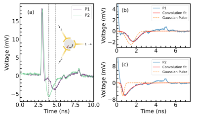
Now, let’s look at the time domain results. The EMP wave packet is capacitively excited by a voltage step across the capacitor at the input port, propagating along the edge of mesa, and then capacitively coupled out through the output port capacitor. The voltage signal is amplified by a cryogenic high electron mobility transistor (HEMT) amplifier and probed by an oscilloscope as a function of time. The rise time of the voltage step varies from 100 ps to 1 ns, leading to a spatial width of the EMP wave packet in the range of , given that the phase velocity of EMP is m/s. Figure 3a plots the time-dependent voltage traces for the m sample, which has a perimeter of 628 m. The EMP wave packet was injected through the ports 2 and 3, respectively, and measured at the port 1 (inset of Fig. 3a). The measured signal consists of two distinct components, a spike with zero-time delay arising from the cross-talk through the detection circuit, and followed by a pronounced dip that shows a port-dependent delay.
The time delay between the two dips correlates with the propagation time of the EMP over a distance of approximately of the perimeter along the boundary of the mesa. Using the analytical method presented in Ref. 12, we fitted the dip component with a convolution integral of a negative Gaussian function and an exponential response function , where ns is the time constant of the detection circuit (Figs. 3 b and c). Here, the EMP wave packet is approximated as a negative Gaussian response due to the fact that the plasmon-transport induced dip is very close to the cross-talk spike, making the differential Gaussian profile undiscernible. Another way of extracting the time of flight of EMP propagation is described in Section IV of the SM and leads to the same result.
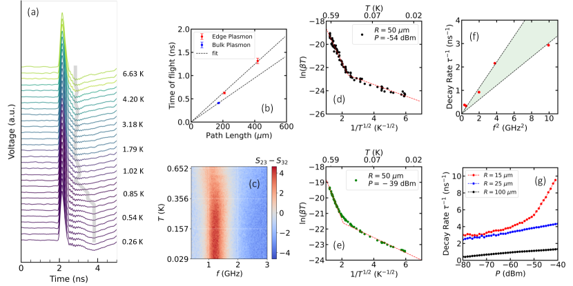
Next, we focus on the temperature dependence of the time domain measurements to reveal an edge-to-bulk transition. Figure 4a presents the voltage traces for the m sample measured as a function of temperature from 12 mK to 6.6 K. For K, the edge state is no longer quantized and plasmons start to propagate in the bulk. [2] As the bulk plasmon propagation undergoes a path along the mesa diameter, they appear as a shorter pulse delay compared with the path P1 along the perimeter. The time of flight for both edge and bulk plasmons is plotted in Fig. 4b, from which the velocity of the wave packet is determined to be m/s and m/s for the edge and bulk plasmons, respectively. The plasmon wave packet velocity is 10 times higher than the drift velocity , consistent with the expected collective oscillation nature of EMPs.[12]
II.5 EMP decay mechanism
Finally, we investigate the EMP decay in disk shaped QAH samples to understand the plasmon dissipation mechanism. Figure 4c shows the difference response as a function of the frequency while sweeping the temperature from 29 mK to 0.652 K. The input port power is kept at dBm. A decrease in frequency and the broadening of the resonant bandwidth have been observed upon increasing the temperature. We can estimate the quality factor from the resonant frequency divided by the full width at half maximum () of the resonance curve: . The standard Lorentzian lineshape fitting to the EMP resonance allows us to obtain the non-reciprocity decay time versus , as listed in Table SI. The observed effect can be explained as the result of the enhanced scattering between the EMP and the dissipative channels in the bulk region that grow with increasing temperature.
The EMP decay mechanism in a QAH system can be quantitatively explained by the coupling of edge states to the charge puddles in the bulk. A three-port Hall circulator model [3, 5] has been used to simulate the EMP decay in a QH system, with a decay rate given by , where is a constant and follows the variable range hopping (VRH) law . [19] Because a QAH system possesses a similar topology and bulk-boundary correspondence as a QH system,[20] we apply the same model to analyze the temperature dependence of the non-reciprocity decay rate, which is roughly proportional to the EMP decay rate (Fig. S14 c). [19] As shown in Figs. 4 d and e, the versus data shows a linear regime with a steep gradient, followed by a shallow linear regime after a threshold value. For a low power dBm, the best fit gives a characteristic temperature K and K above and below the threshold temperature mK, respectively. For higher dBm, the best fit yields K and K above and below mK, respectively. Raising leads to a lower for the VRH behavior for , showing that the microwave radiation enhances the hopping between dissipative channels that are the main source of decay when the temperature is below 0.7 K. [21]
To further confirm the EMP decay mechanism, we plot the versus for various samples in Fig. 4f. The best fit gives and at low . This value is one order of magnitude higher than that of graphene.[19] From the simplified circuit model including the coupling capacitance in series with the dissipation resistance , the -related term is given by , where is the channel capacitance [19] (also see details of the circuit model simulation in Section VII of SM). The observed dependence of indicates the capacitively and resistively coupled dissipation mechanism exists in the QAH insulator. In addition to the large value, we observed an evolution in with mesa radius upon microwave excitation. As shown in Fig. 4g, the non-reciprocity decay rate increases linearly in the and m samples, whereas in the m sample, increases exponentially in the high power regime, suggesting that a non-linear power-dependent scattering mechanism is introduced when the mesa radius is reduced.
III Discussion and Conclusions
For a QAH system, an insulating bulk state is required for the protection of topological edge states from scattering between opposite edges. In our 6-QL Cr-doped BST sample, the QAH activation gap eV is more than 10 times higher than the applied microwave photon energy, e.g., 4 eV at GHz.[22] However, transport measurements have reported the existence of tens-of-nm size isolated charge puddles arising from the large number of superparamagnetic domains in the bulk region of the sample. [21, 22] At high enough microwave excitation, the hopping between the neighboring puddles can possibly create additional conductive channels that are capacitively and resistively coupled to EMPs. The number of microwave excited conductive puddles is expected to be proportional to the microwave power. As a result, the characteristic temperature for the hopping between puddles will decrease with increasing . This is consistent with our observation that is suppressed with a higher microwave excitation for . As the device radius decreases, the smaller device has a greater chance of forming percolating paths that allow edge-to-edge scattering, due to the shorter edge-to-edge distance and the higher resonant frequency, or equivalently, the higher photon energy. This effect is reflected in the decay rate as being dramatically enhanced in the smallest sample.
In summary, we have studied the dispersion relation of EMPs and their decay in a QAH insulator with microwave transmission measurements and time-resolved measurements. We find the transverse width m of EMP is much wider than the edge channel width reported in the equilibrium transport measurement, which is below tens of nanometers.[22] The wide EMP wave packet width indicates that the EMPs differ from their equilibrium counterparts by the presence of electromagnetic fields that influence the local potentials at the edge. We confirmed the collective nature of the EMPs by showing that the EMP wave packet’s propagation velocity is one order of magnitude higher than its drift velocity. The microwave power dependent decay rate is featured with a characteristic hopping temperature, indicating that VRH is still the dominant dissipation mechanism upon the microwave radiation. From the size and power dependence of the microwave transmission measurements, the non-reciprocity decay time is found to scale with the mesa radius, which points to the enhanced scattering between macroscopically separated edge states as the device shrinks to tens of micrometers. Our results will serve to inspire investigation into designing new device structures, toward the realization of low-loss chiral interconnects based on QAH insulators.
Acknowledgements.
We would like to thank Cianpaolo P. Carosi for helpful discussions, and Kristin Beck for assistance in performing the experiments. This work was performed under the auspices of the US Department of Energy by Lawrence Livermore National Laboratory under Contract No. DE-AC52-07NA27344. The project was supported by the Laboratory Directed Research and Development (LDRD) programs of LLNL (21-ERD-014).The authors also acknowledge support from NSF Convergence Accelerator program under Grant 2040737.References
- Yu et al. [2010] R. Yu, W. Zhang, H.-J. Zhang, S.-C. Zhang, X. Dai, and Z. Fang, “Quantized anomalous hall effect in magnetic topological insulators,” Science (New York, N.Y.) 329, 61—64 (2010).
- Chang et al. [2013] C.-Z. Chang, J. Zhang, X. Feng, J. Shen, Z. Zhang, M. Guo, K. Li, Y. Ou, P. Wei, L.-L. Wang, Z.-Q. Ji, Y. Feng, S. Ji, X. Chen, J. Jia, X. Dai, Z. Fang, S.-C. Zhang, K. He, Y. Wang, L. Lu, X.-C. Ma, and Q.-K. Xue, “Experimental observation of the quantum anomalous hall effect in a magnetic topological insulator,” Science (New York, N.Y.) 340, 167—170 (2013).
- Viola and DiVincenzo [2014] G. Viola and D. P. DiVincenzo, “Hall effect gyrators and circulators,” Phys. Rev. X 4, 021019 (2014).
- Liu, Zhang, and Qi [2016] C.-X. Liu, S.-C. Zhang, and X.-L. Qi, “The quantum anomalous hall effect: Theory and experiment,” Annual Review of Condensed Matter Physics 7, 301–321 (2016).
- Mahoney et al. [2017a] A. C. Mahoney, J. I. Colless, S. J. Pauka, J. M. Hornibrook, J. D. Watson, G. C. Gardner, M. J. Manfra, A. C. Doherty, and D. J. Reilly, “On-chip microwave quantum hall circulator,” Phys. Rev. X 7, 011007 (2017a).
- Mahoney et al. [2017b] A. C. Mahoney, J. I. Colless, L. Peeters, S. J. Pauka, E. J. Fox, X. Kou, L. Pan, K. L. Wang, D. Goldhaber-Gordon, and D. J. Reilly, “Zero-field edge plasmons in a magnetic topological insulator,” Nature Communications 8, 1836 (2017b).
- Wang et al. [2023] T. Wang, C. Wu, M. Mogi, M. Kawamura, Y. Tokura, Z.-X. Shen, Y.-Z. You, and M. T. Allen, “Theory of the microwave impedance microscopy of chern insulators,” (2023), arXiv:2304.09227 [cond-mat.mes-hall] .
- Jin et al. [2016] D. Jin, L. Lu, Z. Wang, C. Fang, J. D. Joannopoulos, M. Soljačić, L. Fu, and N. X. Fang, “Topological magnetoplasmon,” Nat. Commun. 7, 13486 (2016).
- Jin et al. [2019] D. Jin, Y. Xia, T. Christensen, M. Freeman, S. Wang, K. Y. Fong, G. C. Gardner, S. Fallahi, Q. Hu, Y. Wang, L. Engel, Z.-L. Xiao, M. J. Manfra, N. X. Fang, and X. Zhang, “Topological kink plasmons on magnetic-domain boundaries,” Nat. Commun. 10, 4565 (2019).
- Pan et al. [2017] D. Pan, R. Yu, H. Xu, and F. J. García de Abajo, “Topologically protected dirac plasmons in a graphene superlattice,” Nat. Commun. 8, 1243 (2017).
- Jin et al. [2017] D. Jin, T. Christensen, M. Soljačić, N. X. Fang, L. Lu, and X. Zhang, “Infrared topological plasmons in graphene,” Phys. Rev. Lett. 118, 245301 (2017).
- Kumada et al. [2013] N. Kumada, S. Tanabe, H. Hibino, H. Kamata, M. Hashisaka, K. Muraki, and T. Fujisawa, “Topologically protected dirac plasmons in a graphene superlattice,” Nat. Commun. 4, 1363 (2013).
- Okazaki et al. [2022] Y. Okazaki, T. Oe, M. Kawamura, R. Yoshimi, S. Nakamura, S. Takada, M. Mogi, K. S. Takahashi, A. Tsukazaki, M. Kawasaki, Y. Tokura, and N.-H. Kaneko, “Quantum anomalous hall effect with a permanent magnet defines a quantum resistance standard,” Nat. Phys. 18, 25–29 (2022).
- Volkov and Mikhailov [1988] V. A. Volkov and S. A. Mikhailov, “Edge magnetoplasmons - Low-frequency weakly damped excitations in homogeneous two-dimensional electron systems,” Zhurnal Eksperimentalnoi i Teoreticheskoi Fiziki 94, 217–241 (1988).
- Wassermeier et al. [1990] M. Wassermeier, J. Oshinowo, J. P. Kotthaus, A. H. MacDonald, C. T. Foxon, and J. J. Harris, “Edge magnetoplasmons in the fractional-quantum-hall-effect regime,” Phys. Rev. B 41, 10287–10290 (1990).
- Petković et al. [2013] I. Petković, F. I. B. Williams, K. Bennaceur, F. Portier, P. Roche, and D. C. Glattli, “Carrier drift velocity and edge magnetoplasmons in graphene,” Phys. Rev. Lett. 110, 016801 (2013).
- Ashoori et al. [1992] R. C. Ashoori, H. L. Stormer, L. N. Pfeiffer, K. W. Baldwin, and K. West, “Edge magnetoplasmons in the time domain,” Phys. Rev. B 45, 3894–3897 (1992).
- Kumada, Kamata, and Fujisawa [2011] N. Kumada, H. Kamata, and T. Fujisawa, “Edge magnetoplasmon transport in gated and ungated quantum hall systems,” Phys. Rev. B 84, 045314 (2011).
- Kumada et al. [2014] N. Kumada, P. Roulleau, B. Roche, M. Hashisaka, H. Hibino, I. Petković, and D. C. Glattli, “Resonant edge magnetoplasmons and their decay in graphene,” Phys. Rev. Lett. 113, 266601 (2014).
- Kawamura et al. [2017] M. Kawamura, R. Yoshimi, A. Tsukazaki, K. S. Takahashi, M. Kawasaki, and Y. Tokura, “Current-driven instability of the quantum anomalous hall effect in ferromagnetic topological insulators,” Phys. Rev. Lett. 119, 016803 (2017).
- Lippertz et al. [2022] G. Lippertz, A. Bliesener, A. Uday, L. M. C. Pereira, A. A. Taskin, and Y. Ando, “Current-induced breakdown of the quantum anomalous hall effect,” Phys. Rev. B 106, 045419 (2022).
- Qiu et al. [2022] G. Qiu, P. Zhang, P. Deng, S. K. Chong, L. Tai, C. Eckberg, and K. L. Wang, “Mesoscopic transport of quantum anomalous hall effect in the submicron size regime,” Phys. Rev. Lett. 128, 217704 (2022).
- Pan et al. [2020] L. Pan, X. Liu, Q. L. He, A. Stern, G. Yin, X. Che, Q. Shao, P. Zhang, P. Deng, C.-Y. Yang, B. Casas, E. S. Choi, J. Xia, X. Kou, and K. L. Wang, “Probing the low-temperature limit of the quantum anomalous hall effect.” Sci Adv. 6, 3595 (2020).