All-Optical Spin Initialization via a Cavity Broadened Optical Transition in On-Chip Hybrid Quantum Photonics
Abstract
Hybrid quantum photonic systems connect classical photonics to the quantum world and promise to deliver efficient light-matter quantum interfaces while leveraging the advantages of both, the classical and the quantum, subsystems. However, combining efficient, scalable photonics and solid state quantum systems with desirable optical and spin properties remains a formidable challenge. In particular the access to individual spin states and coherent mapping to photons remains unsolved for these systems. In this letter, we demonstrate all-optical initialization and readout of the electronic spin of a negatively-charged silicon-vacancy center in a nanodiamond coupled to a silicon nitride photonic crystal cavity. We characterize relevant parameters of the coupled emitter-cavity system and determine the silicon-vacancy center’s spin-relaxation and spin-decoherence rate. Our results mark an important step towards the realization of a hybrid spin-photon interface based on silicon nitride photonics and the silicon-vacancy center’s electron spin in nanodiamonds with potential use for quantum networks, quantum communication and distributed quantum computation.
Quantum applications, such as quantum networks and quantum repeaters, rely on efficient mapping of quantum information between stationary qubits and flying qubits [1, 2, 3]. While photons are a natural choice for flying qubits, since they interact weakly with their environment [4], numerous candidates for stationary qubits are under investigation with individual strengths and weaknesses. Hybrid quantum photonics offers a unique route to efficiently interface stationary to flying qubits, by combining individually optimized photonic and quantum systems. The negatively-charged silicon-vacancy (SiV-) center in diamond is of particular interest, since its defect symmetry enables to retain excellent optical properties even in diamonds with sizes below the optical wavelengths [5], so-called nanodiamonds, enabling two-photon interference from SiV- centers in remote NDs [6]. Hybrid quantum photonics [7, 8], which inherits the advantages of its constituents, is constructed by means of pick and place transfer for evanescent coupling [9, 10], as well as for intrinsic coupling, positioning the quantum emitter in the field maximum of the photonic device [11]. Furthermore, the integration yield has been increased towards large numbers of individually addressable quantum emitters by lithographic positioning [12] or designer nanodiamonds [13]. However, until today access to stationary qubits was not demonstrated in coherent hybrid quantum photonics.
Here, we propose an ND-hosted SiV- center’s electron spin as a stationary qubit and experimentally demonstrate its access in hybrid quantum photonics entailing a number of advantages.
SiV- center in NDs are accompanied with a potential increase in spin coherence through modification of the phonon density of states [14] or through strain [15]. One dimensional photonic crystal cavities enable coherent and efficient exchange of quantum information between stationary qubits and flying qubits in the framework of cavity quantum electrodynamics (cQED) [16], while offering scalability and a small technological footprint on chip.
Our photonic base material is silicon nitride (Si3N4), which offers scalable fabrication and access to many key elements for quantum nodes integrated on a single chip [17]. The one dimensional PCCs employed herein are formed in a single mode Si3N4 waveguide on top of SiO2 with periodic elliptical holes patterned into the waveguide. These periodic holes are interleaved by a hole defect in the center of the cavity, leading to localized modes within the structure and serving as target region for ND placement. At this center point, another single mode Si3N4 waveguide crosses the cavity waveguide orthogonally, being optimized for off-resonant excitation of the SiV- centers. Each of the two waveguides are equipped with efficient broadband out-of-plane couplers [18] to interface the nanostructure with Gaussian optics. For further details on the device see Supplemental Material [19].

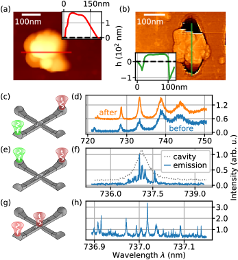
Start of the assembly of our hybrid emitter-cavity system is identifying suitable SiV- center hosting NDs at room temperature via confocal microscopy. The procedure and ND synthesis is described in the Supplemental Material [19]. Suitable candidates are transferred to the PCC by AFM pick and place, following the method in reference [11]. In order to overcome limitations of evanescent coupling, the ND of choice [Fig. 1 (a)] is placed inside a centered PCC hole [Fig. 1 (b)]. After transfer the ND is well embedded, as verified by its AFM height cross section [Fig. 1 (b), inset]. The whole ND assembly does not alter the cavity properties, which we probe utilizing the Si3N4 inherent background fluorescence and the broadband out-of-plane couplers. A green laser is directed onto one of the cavity couplers and excites Si3N4 background fluorescence which is modulated by the cavity when collected at the opposing coupler [Fig. 1 (c)]. Quality factors of the resonance modes, blue detuned from , remain at while the resonance position is nearly unchanged after the assembly [Fig. 1 (d)]. Further details see Supplemental Material [19].
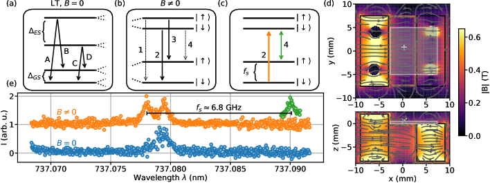
Successful placement of SiV- centers is verified at cryogenic temperatures () by off-resonant excitation via the pump waveguide and fluorescence collection at one of the cavity couplers [Fig. 1 (e)] revealing cavity channeled fluorescence [Fig. 1 (f)]. Alternatively a scanable titanium-sapphire laser is coupled into the cavity and fluorescence is detected from the SiV- center phonon sideband at the cavity center in a photoluminescence excitation (PLE) experiment [Fig. 1 (g)]. An exemplary measurement is seen in Fig. 1 (h) revealing multiple peaks, corresponding to the laser hitting resonance with strain shifted SiV- centers in the ND. Strain alters the SiV- center’s ground- () and excited state () splitting [Fig. 2 (a)] as well as the weighted central wavelength (zero phonon line) of the optical transitions [20, 5], which allows us to address individual SiV- centers.

The SiV- center’s spin-orbit eigenstates, connected by these optical transitions, are spin degenerate in zero magnetic field [22, 23, 24]. In a static magnetic field each eigenstate splits up due to the spin-1/2 nature of the SiV- center. The resulting spin-sublevels are denoted and herein [Fig. 2 (b)]. Transitions between these states are labeled in Fig. 2 (b) and are apparent for each of the optical transitions . Here, the magnetic field is generated by a permanent neodymium magnet assembly, with simulated field strength above [Fig. 2 (d)]. The largest field component lies along the axis at the location of the PCC (see Supplemental Material [19]) which ensures that the magnetic field is parallel to well coupled SiV- centers with their dipole axis parallel to the transverse electric (TE) cavity mode. Alignment of the magnetic field to the SiV- center symmetry axis improves parameters, such as the spin-state purity [22] and the spin relaxation time which influences the cyclicity of the optical transitions [25]. Transition and potentially posses long cyclicity and connect levels of equal spin projection, hence also referred to as spin-preserving transitions, while for transition and the spin will be flipped (spin-flipping). The spin splitting in the ground- and excited state depends on the spin- as well as the orbital degree of freedom, where the latter is larger in the excited state [22]. Consequently, transition 2 and 3 are spectrally separated enabling all-optical electron spin access [24]. The intensity ratio of spin-flipping and spin-preserving transitions depends on the magnetic field alignment relative to the symmetry axis of the SiV- center, with the spin-flipping transition intensity being minimized for parallel alignment [24]. In this case [Fig. 2 (e)] one can probe and reveal the spin-flipping transition by continuously driving one of the spin-preserving transitions while sweeping a second laser’s frequency [Fig. 2 (c)]. The respective frequency difference yields the spin splitting which is in agreement with the magnetic field simulations of Fig. 2 (d).

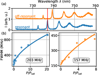
To determine the relevant cQED parameter set {, , } the linewidth for both spin-preserving transitions is measured at varying probe intensities on- and off-resonant with the cavity resonance [Fig. 3]. Extrapolating to zero power according to [26] mitigates any influence of power broadening. Tuning the cavity resonance frequency is realized by controlled freezing of to the PCC [27], shifting the cavity resonances to longer wavelengths. Extracting from the extrapolated zero power value yields at a cavity detuning of [Fig. 3, orange]. This value is consistent with the Fourier-Transform limit of the SiV- center in NDs, where lifetimes in the range from to had been observed at room temperature [28]. The cavity decay rate is determined by the Lorentzian line shape of the resonance resulting in . From the zero power extrapolated Purcell broadened linewidth [Fig. 3 (b), orange] measured with the cavity in resonance () [Fig. 3 (a), blue], we can infer the cooperativity [29] to be translating to a single-photon Rabi frequency for the spin-preserving transitions. The complete cQED parameter set reads

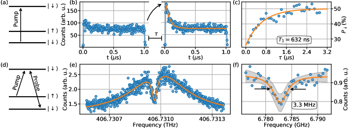
All-optical spin access is realized by optical pumping on one of the spin-preserving transitions [Fig. 4 (a)], starting from equal population in and in thermal equilibrium at and a spin splitting of . During a -long laser pulse [Fig. 4 (b), right], this thermal equilibrium is disturbed by laser-induced optical spin pumping via the spin-flipping transition, depopulating the level . The fluorescence, collected in the phonon sideband, exponentially decays on a timescale of , corresponding to the spin initialization time. The steady state reached towards the end of the laser pulse yields a a final population in the spin-state with a fidelity of , extracted from the ratio of steady state to peak signal. By applying consecutive laser pulses with a varying inter pulse delay, the characteristic relaxation time for the spin-state can be retrieved from an exponential fit of the corresponding initial peak heights [Fig. 4 (c)] which yields . is typically limited due to non-perfect alignment of the SiV- center symmetry axis and the magnetic field, which in our case indicates potential improvement in the coupling strength to the PCC. As outlined earlier, ideally the magnetic field, the SiV- center symmetry axes and the TE mode are co-linear. However, in the given configuration we attribute a decreased to a non-zero z-component () of the magnetic field (see Supplemental Material [19]). With vector control of the magnetic field, the misalignment could be determined and optimized by means of AFM nanomanipulation. In addition to the spin relaxation time , the dephasing rate is of key interest, being the timescale dictating operations on the electronic spin. To probe , a coherent population trapping (CPT) experiment is carried out where two laser fields are simultaneously applied to the SiV- center connecting a spin-preserving and spin-flipping transition in a -type system [Fig. 4 (d)]. When both lasers fulfill the Raman-condition at zero detuning a coherent dark state is formed leading to a dip in fluorescence signal [Fig. 4 (e)]. The dip width is a direct measure of [24] when ensuring phase coherence of the laser fields and excluding power-broadening. This is realized by generating sidebands through microwave drive of an EOM and minimizing the excitation power. The dip width was measured to be as narrow as , which translates to .
In conclusion, we demonstrate the fundamental step for an on-chip hybrid spin-photon interface based on the electronic spin of a SiV- center in NDs and Si3N4 photonics. We achieve a cooperativity of and single-photon Rabi frequency of which both could be further improved by increasing the ratio of factor to mode volume. The simultaneous requirements set herein for spin access and proper optical coupling to the PCC restricts us to a small number of SiV- centers within the ND. Using a higher density of SiV- centers or decreasing the crystal strain, which has direct influence on the possibility for optical spin access [20], could increase the number of SiV- center candidates fulfilling both criteria. A further boost in coupling can be envisioned with additional alterations in the cavity design, or additional optimization through nanomanipulation steps [30] for dipole alignment. With the above turning nobs at hand, cooperativities well above one are within close reach. The accomplished spin initialization fidelity of and the spin relaxation time of of our cavity coupled SiV- center could be improved by alignment of the magnetic field to the SiV- center symmetry axis through vector control. This should increase the spin relaxation time to orders of [24, 31] and enables long cyclicity of the spin-preserving transitions giving access to single-shot readout [32], while also increasing the upper bound for the spin coherence time . The measured spin dephasing rate of is in the range of values obtained for bulk diamond by optically detected magnetic resonance at in a bath cryostat [31], suggesting the feasibility of integrating SiV- centers in NDs with potentially improved spin properties [14]. Implementation of on-chip microwave structures to coherently control the electronic spin, or techniques relying on all optical driving [33, 34], together with above-mentioned improvements leading to cooperativities well above one could enable spin-photon entangling gates based on spin-dependent cavity reflection signal [35, 36].
Acknowledgements.
The project was funded by the BMBF/VDI in Project HybridQToken. A.K. acknowledges support of the Baden-Wuerttemberg Stiftung gGmbH in Project No. BWST-ISF2018-008. The AFM was funded by the DFG, we thank Prof. Kay Gottschalk for the support. N.L. acknowledges support of the IQST. The authors thank V.A. Davydov for synthesis and processing of the nanodiamond material, and P. Maier for production of the FIB markers. D.W. acknowledges funding from the Deutsche Forschungsgemeinschaft (CRC 1459). H.G. acknowledges financial support of the Studienstiftung des deutschen Volkes. Experiments have been orchestrated by the open-source software Qudi [37].References
- Kimble [2008] H. J. Kimble, The quantum internet, Nature 453, 1023 (2008).
- Wehner et al. [2018] S. Wehner, D. Elkouss, and R. Hanson, Quantum internet: A vision for the road ahead, Science 362, eaam9288 (2018).
- Ruf et al. [2021] M. Ruf, N. H. Wan, H. Choi, D. Englund, and R. Hanson, Quantum networks based on color centers in diamond, Journal of Applied Physics 130, 070901 (2021).
- Northup and Blatt [2014] T. E. Northup and R. Blatt, Quantum information transfer using photons, Nature Photon 8, 356 (2014).
- Rogers et al. [2019] L. J. Rogers, O. Wang, Y. Liu, L. Antoniuk, C. Osterkamp, V. A. Davydov, V. N. Agafonov, A. B. Filipovski, F. Jelezko, and A. Kubanek, Single SiV- Centers in Low-Strain Nanodiamonds with Bulklike Spectral Properties and Nanomanipulation Capabilities, Phys. Rev. Applied 11, 024073 (2019).
- Waltrich et al. [2023] R. Waltrich, M. Klotz, V. N. Agafonov, and A. Kubanek, Two-photon interference from silicon-vacancy centers in remote nanodiamonds, Nanophotonics 10.1515/nanoph-2023-0379 (2023).
- Kubanek et al. [2022] A. Kubanek, A. P. Ovvyan, L. Antoniuk, N. Lettner, and W. H. P. Pernice, Hybrid Quantum Nanophotonics—Interfacing Color Center in Nanodiamonds with Si3N4-Photonics, in Progress in Nanophotonics 7, Topics in Applied Physics, edited by T. Yatsui (Springer International Publishing, Cham, 2022) pp. 123–174.
- Sahoo et al. [2023] S. Sahoo, V. A. Davydov, V. N. Agafonov, and S. I. Bogdanov, Hybrid quantum nanophotonic devices with color centers in nanodiamonds [Invited], Opt. Mater. Express, OME 13, 191 (2023).
- Schell et al. [2011] A. W. Schell, G. Kewes, T. Schröder, J. Wolters, T. Aichele, and O. Benson, A scanning probe-based pick-and-place procedure for assembly of integrated quantum optical hybrid devices, Review of Scientific Instruments 82, 073709 (2011).
- Fehler et al. [2020] K. G. Fehler, A. P. Ovvyan, L. Antoniuk, N. Lettner, N. Gruhler, V. A. Davydov, V. N. Agafonov, W. H. P. Pernice, and A. Kubanek, Purcell-enhanced emission from individual SiV- center in nanodiamonds coupled to a Si3N4-based, photonic crystal cavity, Nanophotonics 9, 3655 (2020).
- Fehler et al. [2021] K. G. Fehler, L. Antoniuk, N. Lettner, A. P. Ovvyan, R. Waltrich, N. Gruhler, V. A. Davydov, V. N. Agafonov, W. H. P. Pernice, and A. Kubanek, Hybrid Quantum Photonics Based on Artificial Atoms Placed Inside One Hole of a Photonic Crystal Cavity, ACS Photonics 8, 2635 (2021).
- Schrinner et al. [2020] P. P. J. Schrinner, J. Olthaus, D. E. Reiter, and C. Schuck, Integration of Diamond-Based Quantum Emitters with Nanophotonic Circuits, Nano Lett. 20, 8170 (2020).
- Ngan et al. [2023] K. Ngan, Y. Zhan, C. Dory, J. Vučković, and S. Sun, Quantum Photonic Circuits Integrated with Color Centers in Designer Nanodiamonds (2023), arxiv:2307.13309 [physics, physics:quant-ph] .
- Klotz et al. [2022] M. Klotz, K. G. Fehler, R. Waltrich, E. S. Steiger, S. Häußler, P. Reddy, L. F. Kulikova, V. A. Davydov, V. N. Agafonov, M. W. Doherty, and A. Kubanek, Prolonged Orbital Relaxation by Locally Modified Phonon Density of States for the SiV- Center in Nanodiamonds, Phys. Rev. Lett. 128, 153602 (2022).
- Sohn et al. [2018] Y.-I. Sohn, S. Meesala, B. Pingault, H. A. Atikian, J. Holzgrafe, M. Gündoğan, C. Stavrakas, M. J. Stanley, A. Sipahigil, J. Choi, M. Zhang, J. L. Pacheco, J. Abraham, E. Bielejec, M. D. Lukin, M. Atatüre, and M. Lončar, Controlling the coherence of a diamond spin qubit through its strain environment, Nat Commun 9, 1 (2018).
- Ritter et al. [2012] S. Ritter, C. Nölleke, C. Hahn, A. Reiserer, A. Neuzner, M. Uphoff, M. Mücke, E. Figueroa, J. Bochmann, and G. Rempe, An elementary quantum network of single atoms in optical cavities, Nature 484, 195 (2012).
- Blumenthal et al. [2018] D. J. Blumenthal, R. Heideman, D. Geuzebroek, A. Leinse, and C. Roeloffzen, Silicon Nitride in Silicon Photonics, Proceedings of the IEEE 106, 2209 (2018).
- Gehring et al. [2019] H. Gehring, A. Eich, C. Schuck, and W. H. P. Pernice, Broadband out-of-plane coupling at visible wavelengths, Opt. Lett., OL 44, 5089 (2019).
- [19] See Supplemental Material at [URL will be inserted by publisher] for details on the setup, device assembly, nanodiamond and sample fabrication and magentic field components, which includes Refs. [38-39].
- Meesala et al. [2018] S. Meesala, Y.-I. Sohn, B. Pingault, L. Shao, H. A. Atikian, J. Holzgrafe, M. Gündoğan, C. Stavrakas, A. Sipahigil, C. Chia, R. Evans, M. J. Burek, M. Zhang, L. Wu, J. L. Pacheco, J. Abraham, E. Bielejec, M. D. Lukin, M. Atatüre, and M. Lončar, Strain engineering of the silicon-vacancy center in diamond, Phys. Rev. B 97, 205444 (2018).
- Ortner and Coliado Bandeira [2020] M. Ortner and L. G. Coliado Bandeira, Magpylib: A free Python package for magnetic field computation, SoftwareX 11, 100466 (2020).
- Hepp et al. [2014] C. Hepp, T. Müller, V. Waselowski, J. N. Becker, B. Pingault, H. Sternschulte, D. Steinmüller-Nethl, A. Gali, J. R. Maze, M. Atatüre, and C. Becher, Electronic Structure of the Silicon Vacancy Color Center in Diamond, Physical Review Letters 112, 10.1103/PhysRevLett.112.036405 (2014).
- Müller et al. [2014] T. Müller, C. Hepp, B. Pingault, E. Neu, S. Gsell, M. Schreck, H. Sternschulte, D. Steinmüller-Nethl, C. Becher, and M. Atatüre, Optical signatures of silicon-vacancy spins in diamond, Nat Commun 5, 3328 (2014).
- Rogers et al. [2014] L. J. Rogers, K. D. Jahnke, M. H. Metsch, A. Sipahigil, J. M. Binder, T. Teraji, H. Sumiya, J. Isoya, M. D. Lukin, P. Hemmer, and F. Jelezko, All-Optical Initialization, Readout, and Coherent Preparation of Single Silicon-Vacancy Spins in Diamond, Phys. Rev. Lett. 113, 263602 (2014).
- Pingault et al. [2014] B. Pingault, J. N. Becker, C. H. H. Schulte, C. Arend, C. Hepp, T. Godde, A. I. Tartakovskii, M. Markham, C. Becher, and M. Atatüre, All-Optical Formation of Coherent Dark States of Silicon-Vacancy Spins in Diamond, Phys. Rev. Lett. 113, 263601 (2014).
- Siegman [1986] A. E. Siegman, Lasers (University Science Books, 1986).
- Mosor et al. [2005] S. Mosor, J. Hendrickson, B. C. Richards, J. Sweet, G. Khitrova, H. M. Gibbs, T. Yoshie, A. Scherer, O. B. Shchekin, and D. G. Deppe, Scanning a photonic crystal slab nanocavity by condensation of xenon, Appl. Phys. Lett. 87, 141105 (2005).
- Lindner et al. [2018] S. Lindner, A. Bommer, A. Muzha, A. Krueger, L. Gines, S. Mandal, O. Williams, E. Londero, A. Gali, and C. Becher, Strongly inhomogeneous distribution of spectral properties of silicon-vacancy color centers in nanodiamonds, New J. Phys. 20, 115002 (2018).
- Janitz et al. [2020] E. Janitz, M. K. Bhaskar, and L. Childress, Cavity quantum electrodynamics with color centers in diamond, Optica 7, 1232 (2020).
- Häußler et al. [2019] S. Häußler, L. Hartung, K. G. Fehler, L. Antoniuk, L. F. Kulikova, V. A. Davydov, V. N. Agafonov, F. Jelezko, and A. Kubanek, Preparing single SiV- center in nanodiamonds for external, optical coupling with access to all degrees of freedom, New J. Phys. 21, 103047 (2019).
- Metsch et al. [2019] M. H. Metsch, K. Senkalla, B. Tratzmiller, J. Scheuer, M. Kern, J. Achard, A. Tallaire, M. B. Plenio, P. Siyushev, and F. Jelezko, Initialization and Readout of Nuclear Spins via a Negatively Charged Silicon-Vacancy Center in Diamond, Phys. Rev. Lett. 122, 190503 (2019).
- Sukachev et al. [2017] D. D. Sukachev, A. Sipahigil, C. T. Nguyen, M. K. Bhaskar, R. E. Evans, F. Jelezko, and M. D. Lukin, Silicon-Vacancy Spin Qubit in Diamond: A Quantum Memory Exceeding 10 ms with Single-Shot State Readout, Phys. Rev. Lett. 119, 223602 (2017).
- Debroux et al. [2021] R. Debroux, C. P. Michaels, C. M. Purser, N. Wan, M. E. Trusheim, J. Arjona Martínez, R. A. Parker, A. M. Stramma, K. C. Chen, L. de Santis, E. M. Alexeev, A. C. Ferrari, D. Englund, D. A. Gangloff, and M. Atatüre, Quantum Control of the Tin-Vacancy Spin Qubit in Diamond, Phys. Rev. X 11, 041041 (2021).
- Becker et al. [2018] J. N. Becker, B. Pingault, D. Groß, M. Gündoğan, N. Kukharchyk, M. Markham, A. Edmonds, M. Atatüre, P. Bushev, and C. Becher, All-Optical Control of the Silicon-Vacancy Spin in Diamond at Millikelvin Temperatures, Phys. Rev. Lett. 120, 053603 (2018).
- Nguyen et al. [2019a] C. T. Nguyen, D. D. Sukachev, M. K. Bhaskar, B. Machielse, D. S. Levonian, E. N. Knall, P. Stroganov, C. Chia, M. J. Burek, R. Riedinger, H. Park, M. Lončar, and M. D. Lukin, An integrated nanophotonic quantum register based on silicon-vacancy spins in diamond, Phys. Rev. B 100, 165428 (2019a).
- Nguyen et al. [2019b] C. T. Nguyen, D. D. Sukachev, M. K. Bhaskar, B. Machielse, D. S. Levonian, E. N. Knall, P. Stroganov, R. Riedinger, H. Park, M. Lončar, and M. D. Lukin, Quantum Network Nodes Based on Diamond Qubits with an Efficient Nanophotonic Interface, Phys. Rev. Lett. 123, 183602 (2019b).
- Binder et al. [2017] J. M. Binder, A. Stark, N. Tomek, J. Scheuer, F. Frank, K. D. Jahnke, C. Müller, S. Schmitt, M. H. Metsch, T. Unden, T. Gehring, A. Huck, U. L. Andersen, L. J. Rogers, and F. Jelezko, Qudi: A modular python suite for experiment control and data processing, SoftwareX 6, 85 (2017).
- Eich et al. [2022] A. Eich, T. C. Spiekermann, H. Gehring, L. Sommer, J. R. Bankwitz, P. P. J. Schrinner, J. A. Preuß, S. Michaelis de Vasconcellos, R. Bratschitsch, W. H. P. Pernice, and C. Schuck, Single-Photon Emission from Individual Nanophotonic-Integrated Colloidal Quantum Dots, ACS Photonics 9, 551 (2022).
- Shi et al. [2016] Q. Shi, B. Sontheimer, N. Nikolay, A. W. Schell, J. Fischer, A. Naber, O. Benson, and M. Wegener, Wiring up pre-characterized single-photon emitters by laser lithography, Sci Rep 6, 31135 (2016).