PALS: Distributed Gradient Clocking on Chip
Abstract
Consider an arbitrary network of communicating modules on a chip, each requiring a local signal telling it when to execute a computational step. There are three common solutions to generating such a local clock signal: (i) by deriving it from a single, central clock source, (ii) by local, free-running oscillators, or (iii) by handshaking between neighboring modules. Conceptually, each of these solutions is the result of a perceived dichotomy in which (sub)systems are either clocked or asynchronous. We present a solution and its implementation that lies between these extremes. Based on a distributed gradient clock synchronization algorithm, we show a novel design providing modules with local clocks, the frequency bounds of which are almost as good as those of free-running oscillators, yet neighboring modules are guaranteed to have a phase offset substantially smaller than one clock cycle. Concretely, parameters obtained from a ASIC simulation running at yield mathematical worst-case bounds of on the phase offset for a node grid network.
Index Terms:
on-chip distributed clock generation, gradient clock synchronization, GALS1 Introduction
Consider a circuit of dimension consisting of comparably small modules of normalized dimension that predominately communicate with physically close modules.
Local clock signals. Each circuit module requires a local clock signal to trigger its computational steps. There are two extreme approaches to provide these clock signals: (i) In the synchronous approach, a clock signal is distributed via a clock tree. The clock’s period is chosen to ensure lock-step computational rounds between all modules and, thus, in particular, for communicating modules. (ii) In the asynchronous approach, modules, potentially as small as a single gate, generate the clock signal locally via handshaking with all communication partners.
From the modules’ perspective, both methodologies provide local clock ticks with different guarantees. We focus on three measures: (a) Whether they ensure a round structure, i.e., there is a time-independent tick offset , such that data that is provided at tick is guaranteed to be available at the receiving module at tick . (b) The local skew, i.e., the maximum difference in time between any two ticks at modules that communicate with each other. (c) The waiting time, i.e., the maximal time between two successive ticks. Note that (b+c) combined with a minimal time between successive ticks allows one to construct a round structure.
Limits of the extremes. Ideally, one would wish for a circuit with a round structure, a small local skew, and a small waiting time. While fully synchronous and asynchronous circuits provide a round structure, they have significant local skew or waiting times. The local skew in synchronous circuits has been shown to grow linearly with the circuit width ; see Section 6.3. On the other hand, causal acknowledge chains in asynchronous systems can span the entire system, resulting in waiting times that grow linearly with .
Fully synchronous or asynchronous systems are indeed rare in practice: in current synchronous systems, there are numerous clock domains with asynchronous interfaces in between [2]. Full asynchronous, delay-insensitive circuits [3] suffer from substantial computational limitations [4, 5, 6] and provide no timing guarantees, rendering them unsuitable for many applications. Accordingly, most real-world asynchronous systems will utilize timing assumptions on some components.
A systematic tradeoff: GALS. Globally Asynchronous Locally Synchronous (GALS) systems [7, 8] are a systematic approach between both extremes. Unlike a single synchronous region (clocked circuits), and no clocked regions (delay-insensitive), GALS systems have several clock islands communicating asynchronously via handshakes. If the width of the synchronous islands is small, the clock islands can maintain small skew locally. However, the gain comes at the expense of no round structure: Clocks on different islands may drift apart arbitrarily. Furthermore, communication across clock domains requires passing through synchronizers [8, 9]. Besides the disadvantage of a non-zero probability to cause metastable upsets, the synchronizers incur or more clock cycles of additional communication latency if they are in the data path.
Alternative solutions without synchronizers in the data path have been proposed in [10, 11]. The designs either skip clock cycles or switch to a clock signal shifted by half a period when the transmitter and receiver clock risk violating setup/hold conditions. The signal that indicates this choice (skip/switch) is synchronized without additional latency to the data path. Depending on the implementation and intended guarantees, the additional latency is in the order of a clock period. While this can, in principle, be brought down to the order of setup/hold-windows, such designs would require considerable logical overhead and fine-tuning of delays. An application-level transmission may be delayed by such a time slot. In [10], this additional delay can be up to clock periods when a so-called no-data packet is over-sampled. Further, there is a non-zero probability of metastable upsets, and applying such a scheme has to insert no-data packets periodically.
Finally, consider a potential application that runs on top of such schemes and uses handshaking to make sure all its packets of a (logical) time step have arrived before the next time step is locally initiated. It faces the same problem as a fully asynchronous design: the waiting time grows linearly with the circuit dimension.
Solutions with round structure. A fully synchronous system provides two convenient properties: (i) metastability-free communication, and (ii) a round structure, that is, no need for handshaking between the synchronous islands of a GALS system. Abandoning the synchronous structure leads to the loss of these properties.
Solutions that directly provide a round structure have been proposed. Examples are GALS architectures with pausible clocks [12, 13], distributed clock generation algorithms like DARTS [14] and FATAL [15], wave clock distribution [16], and distributed clocking grids [17]. However, pausible clocks suffer from potentially unbounded waiting times due to metastability, and DARTS and FATAL require essentially fully connected communication networks. The solution in [16] employs analog cross-coupling of clock buffers to distribute a single clock source over a grid network. Here, we show how to design a purely digital system that utilizes an algorithmic approach to synchronize many clock domains. A digital version of the Fairbanks clock generation grid [17] is analyzed in this work and shown to lead to linear waiting times; see Section 6.4.
The PALS approach. In this work, we present a different approach that combines a round structure with low local skew, a low waiting time, and provable absence of metastable-upsets. The PALS approach can be regarded as a drop-in replacement for GALS systems; it uses locally synchronous islands and global communication between islands. It improves over GALS systems by adding a round structure.
Our design is based on the distributed gradient clock synchronization (GCS) algorithm by Lenzen et al. [18], in which the goal is to minimize the worst-case clock skew between adjacent nodes in a network. In our setting, the modules correspond to nodes; an edge connects them if they directly communicate (i.e., exchange data). More precisely, let be the diameter of the network and be the (unintended) drift of the clock of a clocked region, a freely chosen constant, and an upper bound on how precisely the phase difference to neighboring clocked regions is known. Then:
-
•
The synchronized clocks are guaranteed to run at normalized rates between and , i.e., have constant waiting time.
-
•
The local skew is bounded by .
-
•
The global skew, i.e., the maximum phase offset between any two nodes in the system, is .
In other words, the synchronized clocks are almost as good as free-running clocks in a GALS system, with drift , yet the local skew grows only logarithmically in the chip width .
We extend the conference version [1] by an in-depth analysis of the PALS algorithm and additional simulations demonstrating its performance. We further add a comparison to a state-of-the-art clock generation grid [17].
Outline and results. After the introduction in this section, we discuss the computational model in Section 2. In Section 3, we briefly present the GCS algorithm before discussing a variant of the algorithm (called OffsetGCS) used in this work. We break down the OffsetGCS into hardware modules and specify these modules in Section 4. The algorithm carried out by the hardware modules is denoted by ClockedGCS. Our main theorem (Theorem 4.6) states that every hardware system that implements ClockedGCS maintains the skew bounds of the GCS algorithm. An implementation of the hardware modules on register-transfer-level, which we denote by GCSoC, is discussed in Section 5. We conclude this work with simulations of this implementation in Section 6. Implementation and simulation are carried out in the FinFET-based NanGate OCL [19]. For clock sources with an assumed drift of , and , our simple sample implementation guarantees that in the worst case. The resulting local skew is , which is well below a clock cycle. We stress that this enables much faster communication than handshake-based solutions, which incur synchronizer delay. We conclude with a comparison of the performance of our solution by SPICE simulations to a digital version of a Fairbanks grid.
2 Computational Model
Network, Communication, and Timing. The network of communicating synchronous PALS islands is modeled by an undirected graph , where the set of nodes is the set of islands and there is an edge , if and communicate. Edges are bidirectional, i.e., edges and are the same edge. Furthermore, for each , contains edge . The diameter of a network is the maximum distance over all pairs of nodes, where the distance between two nodes is the length of a shortest path connecting those nodes in the network.
We denote real time, i.e., an external reference time for analysis, by Newtonian time. A node has no access to Newtonian time, but has its own (internal) time reference.
Nodes communicate by sending content-less messages, known as pulses. A pulse is sent via broadcast to all neighboring nodes. The message delay is the time a pulse travels between the sender and receiver. It is constrained by a maximum delay and a minimum delay , where is the delay uncertainty. A pulse sent by a node at Newtonian time is received between time and time .
Hardware Clock. Each node can locally measure the progress of time. For example, a node may do this via a local ring oscillator. For the analysis, we abstract any such device by the mathematical concept of a hardware clock. A hardware clock is prone to uncertainty, which we model by a variable rate that may change over time. The uncertainty is called the hardware clock drift (short clock drift). Formally, for each node there is an integrable function called the hardware clock rate. Parameter is an upper bound on the one-sided hardware clock drift of all nodes. The hardware clock rate satisfies for all . The hardware clock value of at time , , is then defined by
where is the initial value of ’s hardware clock at Newtonian time . A node that has measured its hardware clock to advance by knows that the real time difference is in .
Logical Clock. While a hardware clock allows a node to measure time differences, its rate cannot be controlled. The logical clock is a hardware clock that can also be controlled. Indeed, we will use an adjustable ring oscillator in this work as a logical clock. Formally, the local clock signal a node produces is given by , where is the phase (normalized by ) of the clock signal since the first clock tick.111For example, a (perfect, non-drifting) logical clock with frequency has phase at time , and normalized (by ) phase . The logical clock thus advances by a full step of one every time but continuously advances in between. A node’s logical clock is initialized to and follows the hardware clock’s rate but is adjustable by a constant factor. In our algorithm, the logical clock will be implemented by the node’s local adjustable ring oscillator that has only two modes: slow and fast. Their rate differs by factor , slow has (normalized) rate and fast has .
Skew. The skew between two nodes describes the difference in their logical clock values. The upper bound on the skew is a figure of merit for clock synchronization algorithms. We regard two types of skew in a system, the global skew and the local skew.
Definition 2.1 (global and local skew).
The global skew is the maximum skew between any two nodes in the network. Formally, it is defined by
The local skew is the maximum skew between any two neighboring nodes in the network. Formally, it is defined by
Our Goal. Given a network of nodes and the nodes’ local oscillator parameters, the goal is to provide an algorithm (i.e., a circuit) that controls the slow and fast clock speed signals at each node such that small, bounded, local, and global skews are ensured.
3 Algorithm and Skew Bound Guarantees
3.1 Gradient Clock Synchronization
We start by recalling the class of GCS algorithms studied by Lenzen et al. [18].
Intuitively, a GCS algorithm executed by node continuously measures the skew to each neighbor . By a set of rules, the algorithm decides whether to progress the logical clock at a fast or a slow rate. Lenzen et al. showed that such GCS algorithms achieve close synchronization between neighboring nodes in an arbitrary network, i.e., minimize . Let be an upper bound on how precisely the skew between neighbors is known. Provided that the global skew does not exceed a bound of , GCS achieves asymptotically optimal local skew bounded by . In other words, local skew grows only logarithmically in the hop diameter of the network; still, we have clocks that progress at a minimum rate of . The local and global skew bounds are asymptotically optimal [18].
3.2 GCS and OffsetGCS Algorithm
The GCS algorithm by Lenzen et al. computes a logical clock from the hardware clock in two different modes, fast and slow. In slow mode, the logical clock follows the rate of the hardware clock. In fast mode, the logical clock advances at the hardware clock rate and speedup factor . Formally, a node in fast mode advances its logical clock with rate , where is chosen by the designer. A node controls its binary mode signal to adjust its logical clock. In fast mode is set to and, accordingly, in slow mode is set to . The logical clock value of at time with initial value thus is
A node in fast mode must be able to catch up to a node in slow mode. Hence, we pose the constraint that fast mode (without clock drift) can never be slower than slow mode (with clock drift). This can be formalized as
The algorithm specifies two conditions that control when to switch between fast and slow modes. Accordingly, conditions are named fast condition (FC) and slow condition (SC). The algorithm is parameterized by , which determines the synchronization quality.
Definition 3.1 (fast and slow condition).
Let be a positive, non-zero, real number. A node satisfies the fast condition at time if there is a natural number such that both:
| (FC-1) | ||||
| (FC-2) | ||||
Node satisfies the slow condition at time if there is a natural number such that the following conditions hold:
| (SC-1) | ||||
| (SC-2) | ||||
Node satisfies the fast condition if there is at least one node , that is ahead of and no other node behind exceeds the absolute skew between and . The slow condition is satisfied if there is a node behind that has a larger absolute skew to than all nodes ahead of . The thresholds use odd multiples of for the fast condition and even multiples of for the slow condition to ensure mutual exclusion.
If is the node with the largest logical clock value in the network, then all other nodes are behind , they have negative skew. Thus, the slow condition is satisfied for . Accordingly, if is the node with the smallest clock value in the network, then it satisfies the fast condition as all skews to other nodes are positive.
Definition 3.2.
An algorithm is a GCS algorithm with parameters if the following invariants hold, for every node and all times :
| (I1) | |||
| (I2) | |||
| if satisfies FC at time then is in fast mode at time | (I3) | ||
| if satisfies SC at time then is in slow mode at time | (I4) |
Invariant (I2) states that the rate of the logical clock is at least the rate of the hardware clock and at most times the rate of the hardware clock.
Remark.
Every algorithm that meets Definition 3.2 is a GCS algorithm. In this work we focus on the algorithm by Lenzen, Locher, and Wattenhofer [18], which we state in Algorithm 1.
Maximal and Minimal Offsets. The conditions in Definition 3.1 can be reformulated using the maximal and minimal offset. Maximal and minimal offsets at node are given by
| (3) | ||||
| (4) |
The node with the largest offset to is the node that is ahead of the most, and the node with the smallest offset to is the node most behind .
A node satisfies the fast condition if some neighbor reached a (positive) threshold and no other neighbor crossed the corresponding negative offset. If the reached a certain threshold we are certain that some neighbor reached this offset. Accordingly if is larger than the corresponding negative offset, no neighbor crossed the corresponding negative offset. Formally, we replace Eqs. FC-1 and FC-2 and Eqs. SC-1 and SC-2 in Definition 3.1 by
| (FC-1) | |||
| (FC-2) | |||
| (SC-1) | |||
| (SC-2) |
Offset Estimates. Nodes have no access to logical clocks of their neighbors. Hence, precise skews remain unknown to the node. In order to fulfill the invariants of the algorithm a node maintains an estimate of each offset to a neighbor. Offset and skew are the same, we use the terms interchangeably. The offset estimate of node to its neighbor is denoted by . Intuitively, we have . Parameter gives a two-sided bound on the estimates.
| (5) |
Given an estimate of each neighboring clock, the GCS algorithm specifies the fast trigger (FT). Each node determines by FT whether to go fast or slow. A node that satisfies FC must satisfy FT, but a node that satisfies SC must not satisfy FT.
Definition 3.3 (fast trigger).
Let be a positive, non-zero, real number. A node satisfies the fast trigger at time if there is a natural number such that both:
| (FT-1) | ||||
| (FT-2) | ||||
We are now able to state the GCS algorithm in Algorithm 1.Intuitively, the GCS algorithm checks the FT at all times. If satisfies FT then switches to fast mode, otherwise defaults to slow mode.
Remark.
As the decision to run fast or slow is a discrete decision, a circuit implementation will be prone to metastability [20]. We focus on this problem in Section 4.4.
Maximal and Minimal Offset Estimates. The fast trigger of Lenzen et al. can be redefined using the largest and smallest offset estimate of node . We define the maximal and the minimal estimate of ’s offset estimates by
Then, we replace Eqs. FT-1 and FT-2 in Definition 3.3 by
| (FT-1) | ||||
| (FT-2) |
We are thus able to restate the GCS algorithm (Algorithm 1)in Algorithm 2. Rather than quantifiers “exists” and “for all” over all outgoing edges we make use of and . The algorithm, referred to as OffsetGCS, is stated in Algorithm 2.
Next, we show that in OffsetGCS we can also bound the number of thresholds, i.e., we bound the maximum value of in Algorithm 1, line .
Bound on . In case of a bounded local skew, which we will later show to be the case, we can bound the maximal number of steps that need to be measured. Let be the largest skew between two neighbors. Let be the largest number such that . Then, node satisfies the fast trigger at time if there is an such that Eqs. FT-1 and FT-2 hold.
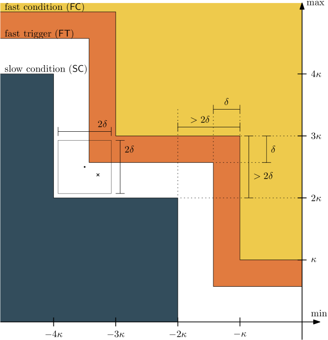
Visualization. In Fig. 1 we depict the conditions of OffsetGCS. Along the axis we mark the offsets, where the -axis marks the maximal and the -axis marks the minimal offset. Conditions FC, SC and FT can be marked as areas. The fast condition, defined by Eqs. FC-1 and FC-2, is marked in yellow. The slow condition, defined by Eqs. SC-1 and SC-2, is marked in blue. The fast trigger, defined by Eqs. FT-1 and FT-2, is a translation of FC by to the left and down. It is marked by the orange are (including the yellow area). We require that (see Theorem 3.5), thus, the gap between FC and SC is larger than .
Fix a node , we mark maximal and minimal offsets as a point . In the GCS algorithm goes to fast mode at any time where falls into the FC (yellow) region. Similarly, if falls into the SC (blue) region, goes to slow mode. In between both regions is free to choose any speed between fast and slow mode. The offset estimates of are given by point , which we mark as a cross. Due to Eq. 5 the cross may fall into the surrounding of . We mark this by a larger box surrounding .
A node that executes OffsetGCS chooses to go to fast or slow mode depending on whether falls into the FT (orange and yellow) region. From the visualization one can see that for any in the FC region, will be within the FT region, and can never cause OffsetGCS to go slow. Similarly any in the SC region can never cause OffsetGCS to go fast.
3.3 Analysis of the OffsetGCS Algorithm
In what follows, we prove that for a suitable choice of parameters (i.e., , , , , and ), OffsetGCS is a GCS algorithm as defined in Definition 3.2. Theorem 3.4 implies that OffsetGCS maintains tight skew bounds. For the proof of Theorem 3.4, we refer the reader to [21].
Theorem 3.4.
Suppose algorithm is a GCS algorithm according to Definition 3.2 with . Then, maintains global and local skew of
either 1) for all if or 2) for sufficiently large , where .
Uncertainty sources in OffsetGCS implementations. In our analysis, we distinguish between two sources of uncertainty: (i) The propagation delay uncertainty . This is the absolute timing variation added to the measurement error due to propagation delays, e.g., wire and gate delays on the path from the clock source to the measurement module. (ii) The measurement error resulting from unknown clock rates. Denote by the time between initiating a measurement and using it to control the logical clock speed. During this time, logical clocks advance at rates that are not precisely known. This adds to the measurement error because the actual difference might increase or decrease compared to the measured difference.
We denote an upper bound on the combined error by ; the relation of to and is elaborated in Section 4.4. Given , we seek to choose as small as possible to obtain a small local skew bound according to Theorem 3.4. In the following, we show constraints on parameters like such that an instance of OffsetGCS, we will refer to it as a particular implementation of OffsetGCS, is a GCS algorithm.
Theorem 3.5.
An implementation of OffsetGCS is a GCS algorithm if for all times it satisfies (i) (ii) (iii) (iv)
Proof.
To show the statement, we verify the conditions of Definition 3.2. By assumption condition (I1) is satisfied. Condition (I2) is a direct consequence of the algorithm specification. For Condition (I3), suppose first that satisfies the fast condition at time . There exists some and neighbor of such that . Therefore, by (5), , so that (FT-1) is satisfied. Further, from the definitions of the local skew and , . Combining the above inequalities yields . By assumption, fulfills . Thus, is set to true.
Similarly, since satisfies the fast condition, all of its neighbors satisfy . Therefore, , hence (FT-2) is satisfied for the same value of . From , it is . Thus, and is set to true. Consequently, runs in fast mode at time .
It remains to show that if satisfies SC at time , it does not satisfy FT at time and is in slow mode. Suppose, for contradiction, that satisfies SC and FT at time . Fix such that SC is satisfied and such that FT is satisfied. Then, by (5) and SC-2,
Thus, by FT-1, Since , the previous expression implies that . Similarly, by (5), SC-1, and FT-2 we obtain , such that, . However, this contradicts . Thus FT cannot be satisfied at time if SC is satisfied at time , as we assumed. ∎
4 Decomposition into Modules
To implement the OffsetGCS algorithm in hardware, we break down the distributed algorithm in this section into circuit modules. Here we are concerned with the clock generation network that comprises an arbitrary number of nodes connected by links. To focus on the clock generation circuitry, we do not discuss the circuitry for the data communication infrastructure that can be implemented using gradient clocking and communication links between clocked modules.
We distinguish between the implementation of a node and the implementation of a link. 222For an in-depth survey of related work and state-of-the-art link-level FIFO buffer controllers, we refer the reader to [22, 23]. Per node, we have a tunable oscillator that is responsible for maintaining the logical clock of a node, and a control module that sets the local clock speed if the fast trigger FT is fulfilled. Per link, we have two phase offset measurement modules, one for each node connected by the link, that measures the clock offset of a node to its neighbor (see Figure 8 for a high-level architecture comprising of the control module, the VCO as the tunable oscillator, and the measurement modules).
Metastability-Containing Implementation. The three modules form a control loop: Skews are measured and fed into the control module, which acts upon the tunable oscillator. Any measurement circuit that round-wise measures a continuous variable, in our case, the skew, and outputs a digital representation can be shown to become metastable [20]. In [24], a technique to compute with such metastable or unstable signals was presented. The term metastability-containing circuit was coined for a circuit that guarantees that the provably minimal amount of metastability carries over from the inputs to the outputs. In this work, we will build on this technique and design the circuitry to be metastability-containing: (i) The measurement circuit outputs the minimal number of metastable outputs, (ii) the controller only produces metastable outputs if its inputs are unstable, and (iii) the tunable oscillator frequency is bounded even in the presence of metastable/unstable signals.
4.1 Tunable Oscillator
The logical clock signal of node is derived from a tunable oscillator. Each node is associated with its own oscillator that can be tuned in its frequency. The tunable oscillator module has one input and one output port. The binary input controls the mode (slow/fast) of the oscillator. The binary output is the oscillator’s binary clock signal whose phase is the logical clock . The oscillator has a maximum response time , by which it is guaranteed to change frequency according to the mode signal. Formally, we require the following conditions to hold:
| (C1) |
If mode signal of node is constantly for time , the oscillator with output is in slow mode at time :
| (C2) |
If a mode signal is constantly for time , the respective oscillator is in fast mode at time :
| (C3) |
Otherwise, the respective oscillator is unlocked at time :
| (C4) |
The requirements on the oscillator are as follows: if the control signal is stable for time, the oscillator needs to guarantee the respective frequency. At any other time, it is not locked to a fixed mode and may run at any frequency between the slowest and fastest possible. In particular, the unlocked mode may be entered when the mode signal is metastable, unstable, or transitioned recently, i.e., an oscillator that satisfies (C4) can cope with meta-/unstable inputs in the sense that it produces stable outputs. We stress that a tunable oscillator satisfying (C4) is not pausible.
It is an essential requirement of the algorithm that the skew between two nodes cannot increase if the algorithm tries to reduce that skew. We maintain the requirement , ensuring that the phase offset between the two clocks cannot increase further when a clock in fast mode is chasing a clock in slow mode.
4.2 Phase Offset Measurement Module
To check whether the FT conditions are met, a node needs to measure the current phase offset to each neighbor . This is achieved by a time offset measurement module between and each neighbor . Node has no direct access to as propagation delays are prone to uncertainty. Hence, a node can only estimate the offset to , where the offset estimate is denoted by .
Inputs to the offset measurement are signals and . The outputs are denoted by for . They represent a unary encoding of of length . As mentioned before, the offset measurement module may produce metastable estimates. We next discuss the module’s specifications.
Thresholds. The algorithm does not require full access to the function , but only to whether has reached one of the thresholds defined by (FT-1) and (FT-2). FT defines infinitely many thresholds, i.e., the algorithm has to check for each whether (FT-1) or (FT-2) is satisfied.
However, practically the system can only measure finitely many thresholds. Since the algorithm guarantees a maximum local skew, there is a maximum until which the algorithm needs to check. Let be the largest number such that , where is the upper bound on the local skew. Then is defined as a binary word of length . The bits are denoted (from left to right) by . For each output bit denotes whether has reached the corresponding threshold. For example, a module with has outputs , , , and corresponding to thresholds , , , and . Each signal is a function of time. For better readability, we omit the function parameter when it is clear from context.
Decision Separator. Any realistic hardware implementation of the offset measurement will have to account for setup/hold times of the registers it uses. We dedicate the decision separator to account for (small) additional setup/hold times, and the effect of a potentially metastable output in case a setup/hold time is violated. A visualization of the decision seperator is given in Fig. 2.
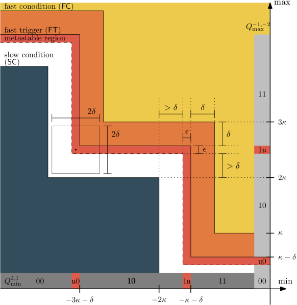
We require that signal is at time if the offset exceeds the th threshold and we require that signal is at time if the offset does not exceed the th threshold. When the offset is close to the threshold (within ), then we allow that is unconstrained, i.e., , where M denotes a metastable or unstable value, e.g., a transition, a glitch, or a value between logical 0 and 1. Formally, we define the module’s outputs to fulfill the following:
Definition 4.1 (decision separator).
Let be a (small) timespan with . At time , we require the following constraints for all . Signal is set to if the offset estimate is larger than .
| (M1) |
Signal is set to if the offset measurement is smaller than .
| (M2) |
Otherwise, is unconstrained, i.e., within .
Figure 3 (middle) shows the timing of signals , , and in relation to the clock of neighbor . When transitions to , the measurement module takes a snapshot of the outputs . In Figure 3 (right), we show two examples.
Figure 3 (left) depicts transitions of the signals . The figure shows increasing (along the -axis), resulting in more and more bits flip to . The decision separator is small enough that no two bits can flip at the same time. If we obtain and for all .
Figure 3 (middle) also depicts transitions of the signals , but along the -axis increases while is fixed. We mark time at which . A digital implementation is only able to measure the offset on a clock event, e.g., a rising clock transition. Hence, will be the time where rises. When , we have that , such that all bits and . As increases, decreases. Hence, in Figure 3, (middle) is a mirror image of (left).


Example 4.2.
Regarding Figure 3 (right), a measurement module with can have output if . The output may become if .
In general, closely synchronized clocks have output . If the clock of is ahead of ’s clock, the measurement contains more s than s. Similarly, if ’s clock is behind the clock of , the outputs contain more s than s. Further, at most one output bit is M at a time if the -regions in Figures 3 (left) and (middle) do not overlap:
Lemma 4.3.
At every time there is at most a single such that is unconstrained.
Proof.
Assume for , that is unconstrained. Then we have that
Hence, for all it holds that , such that, by Definition 4.1, and for all . For all we obtain , as . Thus, by Definition 4.1, . An analogous argument shows that there is only one unconstrained bit if is unconstrained. ∎
Latency. Besides setup/hold times, we have to account further for propagation delays. Let denote the maximum end-to-end latency of the measurement module, i.e., an upper bound on the elapsed time from when is set, to when the measurements are available at the output. More precisely, we require that if is set to for all in , then the corresponding output is as depicted in Figure 3 (right).
4.3 Control Module
Each node is equipped with a control module. Its input is the (unary encoded) time measurement, i.e., bits , for each of ’s neighbors. Output is the mode signal .
The control module is required to set the mode signal according to Algorithm OffsetGCS, i.e., to fast mode if FT is satisfied, otherwise the algorithm defaults to slow mode. Denote by the maximum end-to-end delay of the control module circuit, i.e., the delay between its inputs (the measurement offset outputs) and its output . We then require the following: If OffsetGCS continuously maps the algorithm’s switch to for time , then the output of the control module is at time :
| (L1) |
If OffsetGCS continuously maps the switch to for time , then the output of the control module is at time :
| (L2) |
Otherwise, the output is unconstrained, i.e., within .
Intuitively, FT triggers when there is an offset that crosses threshold and no other offset is below threshold for some . Hence, we select the maximum and minimum of the offsets to all neighbors .
Since the network also includes self-loops (cf. Section 2), each node, conceptually, measures the offset to itself. The offset to self is always . In practice, that means that the maximum only needs to consider neighbors that are ahead and the minimum only needs to consider neighbors that are behind. For , signals indicate whether node is ahead and similar bits indicate whether is behind. Thus, the -bit encodings of maximum () and minimum () are computed as
As FT is satisfied if and are both for any in . Signal is computed by
Metastability-containment. Any metastability-containing implementation of has the following properties: (i) If the slow condition is satisfied, then (ii) if the fast condition is satisfied, then (iii) if no condition is satisfied then may output M. For a formal definition of metastability-containment, we refer the reader to [24]. In Section 5, we present a metastability-containing implementation of the control module.
4.4 ClockedGCS Algorithm
Clocked Algorithm. We are now in the position to assemble the modules into the so-called Clocked Gradient Clock Synchronization (ClockedGCS) algorithm (see Algorithm 3). In the following we prove Theorem 4.6, showing that the ClockedGCS algorithm implements the OffsetGCS algorithm, and hence maintains tight skew bounds. For the measurement module, we defined a possibly metastable assignment if the signal changes within an window during which it is assigned. We denote the assignment with propagation delay and possibly metastable result by .
The ClockedGCS implements the OffsetGCS Algorithm. An essential difference of the ClockedGCS to the continuous time OffsetGCS algorithm is that measurements are performed only at discrete clock ticks. We will, however, show that the clocked algorithm implements the OffsetGCS algorithm, with a properly chosen measurement error that accounts for the fact that we measure clock skew only at discrete points in time rather than continuously.
For that purpose, we denote the maximum end-to-end latency of the computation by . This end-to-end latency combines the delays of the three modules, i.e., . Thus, is the time it takes from a rising clock edge until the oscillator guarantees a stable rate. For a simple implementation, naturally becomes a lower bound on the clock period. Designs with a clock period beyond are possible when buffering measurements and mode signals.
Example 4.4.
A timing diagram with the module outputs and the clock rate is given in Fig. 4. The offset measurement switches from (close to synchronous) to ( lagging behind ) and causes the oscillator to go to fast mode.

We are now in the position to relate the module delays to . We split into two parts, the propagation delay uncertainty and the maximum end-to-end latency. The propagation delay uncertainty accounts for variations in the time a signal takes to propagate from a node’s oscillator to the measurement module of its neighbors. Suppose clock signals arrive at the measurement module with a larger or smaller delay than expected (usually due to variation in the fabrication process or environmental influences), then the module may measure larger or smaller offsets. We denote the propagation delay uncertainty by .
The second source of error is the drift of the clocks when not measuring. The offset is measured once per clock cycle and it is used until the next measurement is made. During this time, the actual offset may change due to different modes and drift of oscillators. We denote the duration of a clock cycle (in slow mode with no drift) by . The maximum difference in rate between any two logical clocks is bounded by . Thus, the maximum change of the offset during a clock cycle is at most
This is the second contribution to the uncertainty of the measurement. Summing up both contributions, the measurement error becomes
Formally, we have the following:
Lemma 4.5.
Let , then ClockedGCS satisfies Inequality (5) at all times .
Proof.
The algorithm measures the offset at each clock tick. Hence, we show that between two clock ticks the uncertainty never grows beyond . Let and be two consecutive clock ticks at node . By the specification above, the measurement at time has precision , such that
During time interval the clock rates may be different for neighbors. The difference between logical clocks grows at most by , such that for ,
Hence, at every time the error is at most , such that Inequality (5) is satisfied. ∎
We are now in the position to prove the section’s main result: under certain conditions on the algorithm’s parameters, ClockedGCS implements OffsetGCS. If, in addition, the algorithm’s parameters fulfill the conditions in Theorem 3.5, it follows that the skew bounds from the GCS algorithm apply to ClockedGCS.
Theorem 4.6.
Proof.
By choosing as in Lemma 4.5, Equation 5 is satisfied. A bounded local skew at all times follows from (C1) and Theorem 3.5. This further implies the finiteness of parameter . For the correct choice of , lines – in ClockedGCS correspond to lines and of OffsetGCS according to (M1) and (M2). Given a metastability-containing implementation, line (respectively ) of ClockedGCS corresponds to line (respectively ) of OffsetGCS according to Boolean logic. Line of ClockedGCS corresponds to lines – of OffsetGCS, where switching to fast (respectively slow) mode is ensured by (L1) and (C2) (respectively (L2) and (C3)). In case of a metastable assignment, (C4) ensures a correct behavior of the oscillator.
5 Hardware Implementation
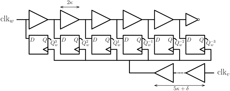
We next present a hardware implementation of the ClockedGCS algorithm, which we refer to as GCSoC. We then discuss its performance and how the system’s parameters affect the achieved skews. For the latter, we designed an ASIC in the FinFET-based NanGate ocl [19] technology. The design is laid out and routed with Cadence Encounter, which is also used for the extraction of parasitics and timing. Local clocks run at a frequency of approximately , controllable within a factor of . We use a larger factor to make the interplay of and better visible. We compile two systems of respectively. nodes connected in a line. To resemble a realistically sparse spacing of clock regions, we placed nodes at distances of . Hence, the PALS systems shown in the simulations are designed to cover floorplans of width and length respectively .
Offset Measurement. Figure 5 shows a linear TDC-based circuitry for the module which measures the time offsets between nodes and . Buffers are used as delay elements for incoming clock pulses. The offset is measured in steps of , hence, buffers in the upper delay line have a delay of . The delay line is tapped after each buffer for corresponding . A chain of flip-flops takes a snapshot of the delay line by sampling the taps. We require and , for all , when and according to (M1) and (M2). Thus, we delay by . The decision separator accounts for the critical setup/hold window of the flip-flop.
Example 5.1.
If both clocks are perfectly synchronized, i.e., , then the state of the flip-flops will be after a rising transition of . Now, assume that clock is ahead of clock , say by a small more than , i.e., . For the moment assuming that we do not make a measurement error, we get . From the delays in Fig. 5 one verifies that in this case, the flip-flops are clocked before clock has reached the second flip-flop with output , resulting in a snapshot of . Likewise, an offset of results in a snapshot of .
Control Module. Given node ’s time offsets to its neighbors in unary encoding, the control module computes the minimal and maximal threshold levels which have been reached. The circuit in Figure 6 implements the control module for neighbors , , and . As described in Section 4.3, we only need to compute the maximal value of bits and the minimal value of bits ; which can be easily computed by an or respectively and over all neighbors.
Given the maximal and minimal values, the circuit in Fig. 6(b) computes FT and sets to if it holds.


Metastability-Containing Control Module. As described in Section 4, the inputs to the control module may be metastable, i.e., unknown or even oscillating signals between ground and supply voltage. It remains for us to show that the control module, given in Figure 6, fulfills specifications (L1) and (L2). In particular, we need to ensure that the specifications are met for metastable inputs.
The circuit in Figure 6 follows from the definition of in Section 4.3, when replacing each conjunction (respectively disjunction) by an and (respectively or) gate. Due to the masking properties of and and or gates, the output can only become metastable when there is an such that one of or is M and the other is or M. This is only the case when Eq. L1 and Eq. L2 do not apply. It follows that the output of the control module can only become metastable when the mode signal is unconstrained and the conditions are met.
Tunable Oscillator. As a local clock source, we use a ring oscillator inspired by the starved inverter ring presented in [25]. We use a ring of inverters, where some inverters being current-starved-inverters, to set the frequency to either fast mode or slow mode. Nominal frequency is around , controllable by a factor via the signal. For our simulations, we choose , assuming a stable oscillator. While this requirement poses a challenge to an oscillator design, it can be relaxed in different ways: (i) By choosing larger parameters and such that their ratio remains fixed, i.e., , this forces us to choose a larger , and hence requires to measure larger time offsets. This is at the cost of a larger skew and circuit (this follows from combining Theorem 3.4, Theorem 3.5, and Lemma 4.5). (ii) By locking the local oscillators to a central quartz oscillator. The problem is different from building a balanced clock tree since the quartz’s skew can be neglected here. (iii) We conjecture that with a refined analysis of the algorithm: rather than absolute drift, the drift with respect to a neighboring oscillator is determinant. Neighboring oscillators show reduced drift due to common cause effects.
The tunable ring oscillator comes with the advantage that for any input voltage it runs at a speed between fast and slow mode, hence, (C4) is satisfied. In the following paragraph, we define an upper bound on such that constraints (C2) and (C3) are satisfied.
Timing Parameters. We next discuss how the modules’ timing parameters relate to the extracted physical timing of the above design.
The time required for switching between oscillator modes is about the delay of the ring oscillator, which in our case is about . An upper bound on the measurement latency () plus the controller latency () is given by a clock cycle () plus the delay () of the circuitry in Figure 6. In our case, delay extraction of the circuit yields . We thus have, .
The uncertainty, , in measuring if has reached a certain threshold is given by the uncertainties in latency of the upper delay chain plus the lower delay chain in Fig. 5. For the described naive implementation using an uncalibrated delay line, this would be problematic: Extracting delays from the design after layout, the constraints from Theorem 3.5 were met for delay uncertainties of , but not for the we targeted. We thus redesigned the Offset Measurement circuit as described in the following.
Improved Offset Measurement. Figure 7 shows an improved TDC-type offset measurement circuit that does not suffer from the problem above. Conceptually, the TDC of the node that measures offsets w.r.t. node is integrated into the local ring oscillator of the neighboring node . If has several neighbors, e.g., up to in a grid, they share the taps but have their own flip-flops within the node .
Figure 7 presents a design for with taps and a single neighbor . In our hardware implementation we set , as even for this is sufficient for networks of diameter up to around (see how to choose this set of thresholds in the specification of this module in Section 4). The gray buffers at the offset measurement taps decouple the load of the remaining circuitry. At the bottom of the ring oscillator, an odd number of starved inverters are used to set the slow or fast mode for node . The delay elements at the top are inverters instead of buffers to achieve a latency of . We inverted the clock output to account for the negated signal at the tap of clock at the top.
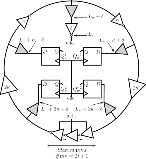
When integrating the measurement into the ring oscillator, the constraints (C2) – (C4) and (M1), (M2) are still met for a suitable choice of . Integration of the TDC into ’s local ring oscillator greatly reduces uncertainties at both ends: (i) the uncertainty at the remote clock port (of node ) is removed to a large extent since the delay elements which are used for the offset measurements are part of ’s oscillator, and (ii) the uncertainty at the local clock port is greatly reduced by removing the delay line of length . The remaining timing uncertainties are the latency from taps to the D-ports of the flip-flops and from clock to the -ports of the flip-flop. Timing extraction yielded in presence of gate delay variations.
Full Hardware Implementation.

We depict in Fig. 8 the schematic of a node with three neighbors. From Theorem 3.5, we obtain and which matched the previously chosen latencies of the delay elements. Applying Theorem 3.4, finally, yields the global and local skew bounds: and . For our design with diameter this makes a maximum global skew of and a maximum local skew of . With regard to diameter , we obtain a maximum global skew of and a maximum local skew of .
As described above, GCSoC satisfies constraints (C2) – (C4), (M1), (M2), (L1), and (L2). Parameters , , and are restricted by the technology. For our choices of , , and GCSoC satisfies the conditions of Theorem 3.5. Thus, from Theorem 4.6 it follows that our implementation maintains the skew bounds of the GCS algorithm.
Corollary 5.2.
Given (C1), GCSoC is an implementation of ClockedGCS. Hence, it maintains global skew and local skew .
Remark.
6 Simulations
We ran spice simulations of the post-layout extracted design with Cadence Spectre. Simulated systems had and nodes arranged in a line, as described in Section 5. We chose a line setup since it allows us to compare local (between neighbors) versus global (typically the line ends) skew best. Nodes are labeled to (respectively ). For the simulations, we set (instead of ), resulting in a slower decrease of skew, to observe better how the skew is removed. Operational corners of the spice simulations were supply voltage and temperature.
Simulation with a small initial skew yields a peak power of during stabilization and an average power of . The performance measure of our system is given by the quality of the local skew. We discuss in detail the local skew for different set-ups in the next section.
6.1 spice Simulations on a Node Topology
Scenarios. We designed three simulation scenarios with different initial skews that demonstrate different properties of the algorithm: ahead: node is initialized with an offset of ahead of all other nodes, behind: node is initialized with an offset of behind all other nodes, and gradient: nodes are initialized with small skews on each edge, that sum up to a large global skew. Simulation time for all scenarios is ( clock cycles).
ahead
behind
gradient
Figure 9(a) depict the local and global skews of all scenarios. Observe that all local skews decrease until they reach less than . The local skew then remains in a stable region. This is well below our worst-case bound of on the local skew. We observe that the global skew slightly increases at the beginning of scenario ahead and after roughly in scenario behind.
One Node Ahead. Figure 10 shows the clock signals of nodes to at three points in time for scenario ahead: (i) shortly after the initialization, (ii) around , and (iii) after . The skews on the three nodes’ edges are depicted in Fig. 9(b).

For the mode signals, in the first scenario, we observe the following: Since node is ahead of nodes and , node ’s mode signal is correctly set to (slow mode) while node and ’s mode signals are set to (fast mode). Node is unaware that node is ahead since it only monitors node . By default, its mode signal is set to slow mode. Node then advances its clock faster than node . When the gap between and is large enough, node switches to fast mode. This configuration remains until nodes and catch up to node , where they switch to slow mode not to overtake node . Again, node sees only node , which is still ahead, and switches to slow mode only after it catches up to .
One Node Behind. The skews on the edges , , and are depicted in Fig. 9(c). We plot the absolute value of the skew, e.g., at roughly node overtakes node . The simulation shows that the algorithm immediately reduces the local skew. After the system reaches a small local skew after , nodes drift relative to each other, e.g., node drifts ahead of node , and node overtakes node . The local skew remains in the stable (oscillatory) state after and does not increase significantly.
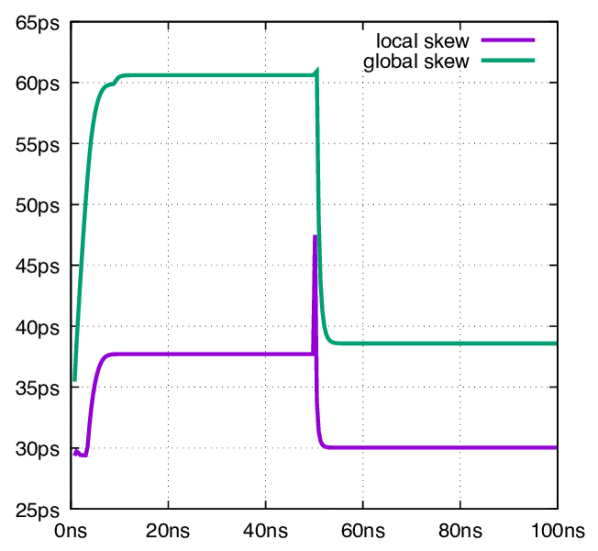
Gradient Skew. The scenario gradient demonstrates how the OffsetGCS algorithm works. It reduces the local skew in steps of (odd multiples of) , as seen in the plot in Fig. 9(d) that looks like a staircase. The algorithm reduces skew on one edge at a time until it reaches the next plateau.
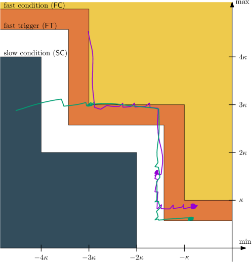
Figure 9(d) demonstrates how skew is removed. OffsetGCS starts by reducing skew on edge until it reaches the plateau of and . One by one it then reduces skew on edges , to until they reach the next plateau. Finally, it reduces the skews one by one (in reverse order) down to a stable range. Figure 11 shows the same trace in a plot similar to Fig. 1.
Remark.
For the sake of a clearly visible convergence of the skew over time, we chose initial skews that are beyond the bound in (C1). Thus, the weaker self-stabilizing bound from Theorem 3.4 applies. All simulations showed convergence to a small local skew despite the less conservative initialization – demonstrating the robustness of our algorithm also to larger initial skews. For our stronger bounds to hold, the reader may consider only a respective postfix of the simulation.
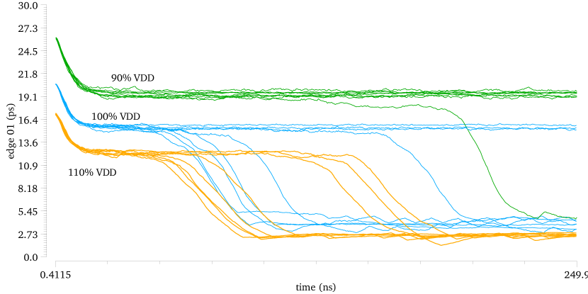
6.2 Process Variations
In order to show resilience of our implementation towards process variations, we introduce variations to the extracted netlist and run further spice simulations. We initialize node 1 with a small offset to nodes 0, 2, and 3. Variations affect the width and length of n-channel and p-channel transistors and the supply voltage, where all parameters are simulated at 90%, 100%, and 110% of their typical value. The resulting skew on edge (0,1) for each simulation is depicted in Fig. 12. The simulations show that our system performs well even under process variations. The local skew after stabilization is below the theoretical bound of .
6.3 Comparison to a Clock Tree
For comparison, we laid out a grid of flip-flops, evenly spread in distance in x and y direction across the chip. The data port of a flip-flop is driven by the or of the up to four adjacent flip-flops. Clock trees were synthesized and routed with Cadence Innovus, with the target to minimize skews. Parameters for delay variations on gates and nets were set to .
For a grid, Innovus reported an area of and power of for the clock tree. Reported numbers for the PALS system, which comprises nodes in a line, are area and power. Numbers for the PALS system do not include the starved inverter ring oscillators. We point out that the size of covers only of the floorplan. The PALS system uses gates from the standard cell library.
The resulting clock skews are presented in Fig. 13. We plotted skews guaranteed by our algorithm for the same grids with parameters extracted from the implementation described in Section 5. Observe the linear growth of the local clock skew measured in the simulation compared to the logarithmic growth of the analytical upper bound on the local skew in our implementation. The figure also shows the simulated skew for a clock tree with delay variations of . This comparison is relevant, as is governed by local delay variations, which can be expected to be smaller than those across a large chip.
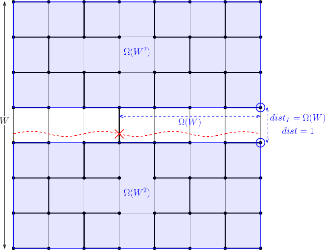
While a priori the observed linear local skew may be due to the tool, it has been shown that no tool can obtain a local skew less than proportional to [26]. This follows from the fact that there are always two neighboring nodes in the grid which are in distance proportional to from each other in the clock tree [26, 27]. Accordingly, uncertainties accumulate in the worst-case fashion to create a local skew which is proportional to . Our algorithm, on the other hand, manages to reduce the local skew exponentially to being proportional to .
To gain intuition on this result, note that there is always an edge that, if removed (see the edge which is marked by an X in Fig. 14), partitions the tree into two subtrees each spanning an area of and hence having a shared perimeter of length . Thus, there must be two adjacent nodes, one on each side of the perimeter, at distance in the tree.
6.4 Comparison to Distributed Clock Generation
We next compare our findings to distributed clock generation schemes. Natural are wait-for-all and wait-for-one, where a node produces its next clock tick once it receives a tick by one or all its neighbors. Both approaches are vulnerable to large local skews, however.
A clever combination of both schemes is used by the clock generation grid by Fairbanks and Moore [17]. In the grid, both approaches alternate for adjacent nodes. For comparison, we simulated a digital abstraction of the clock generation grid. Based on ideas of the lower bound proof for local skews [29], we construct a simulation scenario that demonstrates that large local skew are possible in the clock grid, however.
Clock Generation Grid. The clock generation grid is a self-timed analog circuit that provides local, synchronized clocks. It is based on the Dynamic asP fifo control by Molnar and Fairbanks [30]. While the optimized version of the clock generation grid is an analog implementation that involves rigorous transistor sizing and layout, we focus on a digital version [17] which is easier to adapt and manufacture in a standard design process. We distinguish two types of nodes: pull-up nodes and pull-down nodes (see Fig. 15). On every edge between two nodes, there is a set-reset latch. Pull-up nodes set the latch and pull-down nodes reset the latch. Pull-up nodes compute the logical nor of incoming edges (equivalent to a wait-for-all approach) and set the latch. Pull-down nodes compute the logical and of incoming edges (equivalent to a wait-for-one approach) and reset the latch. The clock of a node is derived by the output of the respective nor or and. The grid’s frequency is easily adjusted by adding a delay between the nodes and the latches.

Setup. We next conducted simulations that examine the behavior of different communication delays. In order to simulate slower communication paths, we add a small capacity () to the communication channel. For simplicity, we differentiate between two delays: fast and slow.
Formally, the algorithm combining wait-for-all and wait-for-one approaches can have a local skew that grows linearly with the network diameter. Through our simulations, we demonstrate that this is indeed possible in the clock generation grid and that OffsetGCS can cope with this situation. The setup of the simulated delays is depicted in Fig. 16: outgoing edges of nodes , , and are fast and edges outgoing from , , , and are slow.

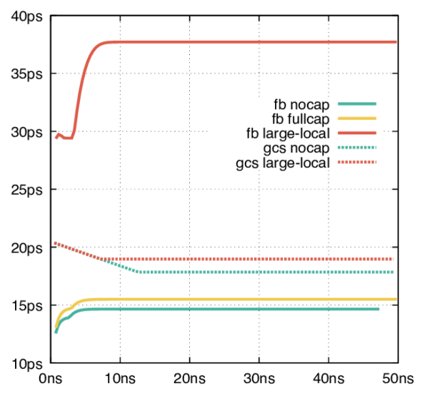
Results for Clock Generation Grid. The digital clock generation grid runs at a frequency of about . By simulations, we determined that an additional capacity of on an edge adds a delay of approximately . We next conducted simulations with three different delay settings: nocap: the grid without additional delays, fullcap: the grid with the capacity added to every edge, and large-local: the grid with the setting from Fig. 16.
Local skews of simulation scenarios nocap, fullcap, and large-local are shown in Fig. 17(a). We observe that the grid achieves a low skew if the delay is uniform on all edges. For scenario nocap (respectively. fullcap) we measure a local skew of (respectively. ) and global skew of (respectively. ). By contrast, the grid experiences poor synchronization for non-uniform delays (large-local) where we obtained a local skew of and a global skew of .
Lower Bound Simulation. In this simulation, we apply ideas from the formal argument for lower bounds on wait-for-all and wait-for-one approaches. The idea is to build up a large global skew and then change the edges’ delays step by step, pushing the global skew onto a single edge. The simulation in Fig. 17(b) shows one of these push-steps. In the first part of the simulation (until ) the system builds up a large local skew. At we switch delays of edges outgoing from nodes and as described in Fig. 16. As expected, the global skew is pushed onto the local skew right after (we measure ). Following the argument of the lower-bound proof, one can repeat the procedure to push the complete global skew (temporarily) onto a single edge.
Comparison to GCSoC. Our clock generation algorithm runs at a frequency of about . By simulations, we measured that the added capacity of adds a delay of approximately . We observed a local skew of and a global skew of in the absence of additional communication delay. This is slightly worse than the local skew of the grid (see Fig. 17(a)). However, by our theoretical findings, our algorithm does not suffer from a large skew in the setting where delays in the center are fast or switched from fast to slow: simulations of Fig. 16 showed a local skew of and a global skew of .
7 Conclusion
The presented ClockedGCS algorithm is a clock synchronization algorithm that provably maintains the skew bounds of the GCS algorithm by Lenzen et al. [18]. The algorithm can be deconstructed into parts that hardware modules can implement. Asymptotically, the algorithm maintains a local skew that is at most logarithmic in the chip’s width, whereas clock trees are shown to perform only linear in the width of the chip.
By simulation, we show that our GCSoC implementation of these modules in a FinFET achieves small skews between neighbors even under process variations. We discuss different simulation setups that show how the algorithm behaves.
In future work, we aim to improve the analysis of the GCS algorithm by showing its correctness for oscillators with less stringent requirements. Additionally, we plan to conduct simulations of a full design, incorporating PVT and PPA experiments, and eventually produce an ASIC chip for comparison to a cutting-edge GALS design.
Acknowledgments
The authors would like to thank the team of EnICS Labs for support and helpful discussions. In particular, we thank Benjamin Zambrano and Itamar Levi, Itay Merlin, Shawn Ruby, Adam Teman, Leonid Yavits. This project has received funding from the European Research Council (ERC) under the European Union’s Horizon 2020 research and innovation programme (grant agreement 716562). This research was supported by the Israel Science Foundation under Grant 867/19 and by the ANR project DREAMY (ANR-21-CE48-0003).
References
- [1] J. Bund, M. Függer, C. Lenzen, M. Medina, and W. Rosenbaum, “PALS: plesiochronous and locally synchronous systems,” in 26th IEEE International Symposium on Asynchronous Circuits and Systems, ASYNC 2020, Salt Lake City, UT, USA, May 17-20, 2020. IEEE, 2020, pp. 36–43. [Online]. Available: https://doi.org/10.1109/ASYNC49171.2020.00013
- [2] H. D. Foster, “Trends in functional verification: a 2014 industry study,” in Proceedings of the 52nd Annual Design Automation Conference, San Francisco, CA, USA, June 7-11, 2015. ACM, 2015, pp. 48:1–48:6. [Online]. Available: https://doi.org/10.1145/2744769.2744921
- [3] A. J. Martin, “Compiling communicating processes into delay-insensitive VLSI circuits,” Distributed Comput., vol. 1, no. 4, pp. 226–234, 1986. [Online]. Available: https://doi.org/10.1007/BF01660034
- [4] ——, “The limitations to delay-insensitivity in asynchronous circuits,” in Beauty is our business. Springer, 1990, pp. 302–311.
- [5] R. Manohar and Y. Moses, “The eventual c-element theorem for delay-insensitive asynchronous circuits,” in 23rd IEEE International Symposium on Asynchronous Circuits and Systems, ASYNC 2017, San Diego, CA, USA, May 21-24, 2017. IEEE Computer Society, 2017, pp. 102–109. [Online]. Available: https://doi.org/10.1109/ASYNC.2017.15
- [6] ——, “Asynchronous signalling processes,” in 25th IEEE International Symposium on Asynchronous Circuits and Systems, ASYNC 2019, Hirosaki, Japan, May 12-15, 2019. IEEE, 2019, pp. 68–75. [Online]. Available: https://doi.org/10.1109/ASYNC.2019.00018
- [7] D. M. Chapiro, “Globally-asynchronous locally-synchronous systems.” Stanford Univ CA Dept of Computer Science, Tech. Rep., 1984.
- [8] P. Teehan, M. R. Greenstreet, and G. G. Lemieux, “A survey and taxonomy of GALS design styles,” IEEE Des. Test Comput., vol. 24, no. 5, pp. 418–428, 2007. [Online]. Available: https://doi.org/10.1109/MDT.2007.151
- [9] R. R. Dobkin, R. Ginosar, and C. P. Sotiriou, “Data Synchronization Issues in GALS SoCs,” in 10th International Symposium on Advanced Research in Asynchronous Circuits and Systems (ASYNC 2004), 19-23 April 2004, Crete, Greece. IEEE Computer Society, 2004, pp. 170–180. [Online]. Available: https://doi.org/10.1109/ASYNC.2004.1299298
- [10] L. R. Dennison, W. J. Dally, and T. Xanthopoulos, “Low-latency plesiochronous data retiming,” in 16th Conference on Advanced Research in VLSI (ARVLSI ’95), March 27-29, 1995, Chapel Hill, North Carolina, USA. IEEE Computer Society, 1995, pp. 304–315. [Online]. Available: https://doi.org/10.1109/ARVLSI.1995.515628
- [11] A. Chakraborty and M. R. Greenstreet, “Efficient self-timed interfaces for crossing clock domains,” in 9th International Symposium on Advanced Research in Asynchronous Circuits and Systems (ASYNC 2003), 12-16 May 2003, Vancouver, BC, Canada. IEEE Computer Society, 2003, pp. 78–88. [Online]. Available: https://doi.org/10.1109/ASYNC.2003.1199168
- [12] K. Y. Yun and R. P. Donohue, “Pausible clocking: A first step toward heterogeneous systems,” in 1996 International Conference on Computer Design (ICCD ’96), VLSI in Computers and Processors, October 7-9, 1996, Austin, TX, USA, Proceedings. IEEE Computer Society, 1996, pp. 118–123. [Online]. Available: https://doi.org/10.1109/ICCD.1996.563543
- [13] X. Fan, M. Krstic, and E. Grass, “Analysis and optimization of pausible clocking based GALS design,” in 27th International Conference on Computer Design, ICCD 2009, Lake Tahoe, CA, USA, October 4-7, 2009. IEEE Computer Society, 2009, pp. 358–365. [Online]. Available: https://doi.org/10.1109/ICCD.2009.5413130
- [14] M. Függer and U. Schmid, “Reconciling fault-tolerant distributed computing and systems-on-chip,” Distributed Comput., vol. 24, no. 6, pp. 323–355, 2012. [Online]. Available: https://doi.org/10.1007/s00446-011-0151-7
- [15] D. Dolev, M. Függer, U. Schmid, and C. Lenzen, “Fault-tolerant algorithms for tick-generation in asynchronous logic: Robust pulse generation,” Journal of the ACM (JACM), vol. 61, no. 5, p. 30, 2014.
- [16] T. C. Fischer, A. K. Nivarti, R. Ramachandran, R. Bharti, D. Carson, A. Lawrendra, V. Mudgal, V. Santhosh, S. Shukla, and T.-C. Tsai, “9.1 D1: A 7nm ML training processor with wave clock distribution,” in 2023 IEEE International Solid-State Circuits Conference (ISSCC). IEEE, 2023, pp. 8–10.
- [17] S. Fairbanks and S. W. Moore, “Self-timed circuitry for global clocking,” in 11th International Symposium on Advanced Research in Asynchronous Circuits and Systems (ASYNC 2005), 14-16 March 2005, New York, NY, USA. IEEE Computer Society, 2005, pp. 86–96. [Online]. Available: https://doi.org/10.1109/ASYNC.2005.29
- [18] C. Lenzen, T. Locher, and R. Wattenhofer, “Tight bounds for clock synchronization,” J. ACM, vol. 57, no. 2, pp. 8:1–8:42, 2010. [Online]. Available: https://doi.org/10.1145/1667053.1667057
- [19] M. G. A. Martins, J. M. Matos, R. P. Ribas, A. I. Reis, G. Schlinker, L. Rech, and J. Michelsen, “Open cell library in 15nm freepdk technology,” in Proceedings of the 2015 Symposium on International Symposium on Physical Design, ISPD 2015, Monterey, CA, USA, March 29 - April 1, 2015, A. Davoodi and E. F. Y. Young, Eds. ACM, 2015, pp. 171–178. [Online]. Available: https://doi.org/10.1145/2717764.2717783
- [20] L. R. Marino, “General theory of metastable operation,” IEEE Trans. Computers, vol. 30, no. 2, pp. 107–115, 1981. [Online]. Available: https://doi.org/10.1109/TC.1981.6312173
- [21] J. Bund, M. Függer, C. Lenzen, M. Medina, and W. Rosenbaum, “PALS: plesiochronous and locally synchronous systems,” CoRR, vol. abs/2003.05542, 2020. [Online]. Available: https://arxiv.org/abs/2003.05542
- [22] D. Konstantinou, A. Psarras, C. Nicopoulos, and G. Dimitrakopoulos, “The mesochronous dual-clock fifo buffer,” IEEE Transactions on Very Large Scale Integration (VLSI) Systems, vol. 28, no. 1, pp. 302–306, 2019.
- [23] J. Bund, M. Függer, C. Lenzen, and M. Medina, “Synchronizer-free digital link controller,” IEEE Transactions on Circuits and Systems I: Regular Papers, vol. 67, no. 10, pp. 3562–3573, 2020.
- [24] S. Friedrichs, M. Függer, and C. Lenzen, “Metastability-containing circuits,” IEEE Trans. Computers, vol. 67, no. 8, pp. 1167–1183, 2018. [Online]. Available: https://doi.org/10.1109/TC.2018.2808185
- [25] D. Ghai, S. P. Mohanty, and E. Kougianos, “Design of parasitic and process-variation aware Nano-CMOS RF circuits: A VCO case study,” IEEE Trans. Very Large Scale Integr. Syst., vol. 17, no. 9, pp. 1339–1342, 2009. [Online]. Available: https://doi.org/10.1109/TVLSI.2008.2002046
- [26] A. L. Fisher and H. T. Kung, “Synchronizing large VLSI processor arrays,” IEEE Trans. Computers, vol. 34, no. 8, pp. 734–740, 1985. [Online]. Available: https://doi.org/10.1109/TC.1985.1676619
- [27] P. Boksberger, F. Kuhn, and R. Wattenhofer, “On the approximation of the minimum maximum stretch tree problem,” Technical report/ETH, Department of Computer Science, vol. 409, 2003.
- [28] M. James, “Linear solver in linear time.” [Online]. Available: https://www.i-programmer.info/news/181-algorithms/5573-linear-solver-in-linear-time.html
- [29] R. Fan and N. A. Lynch, “Gradient clock synchronization,” Distributed Comput., vol. 18, no. 4, pp. 255–266, 2006. [Online]. Available: https://doi.org/10.1007/s00446-005-0135-6
- [30] C. E. Molnar and S. M. Fairbanks, “Control structure for a high-speed asynchronous pipeline,” Aug. 10 1999, US Patent 5,937,177.
![[Uncaptioned image]](/html/2308.15098/assets/x25.jpg) |
Johannes Bund is a post-doc researcher at the Faculty of Engineering at Bar-Ilan University since 2022. He graduated with his M. Sc. studies in 2018 at the Saarland Informatics Campus and Max-Planck Institute for Informatics. In 2018 he joined Christoph Lenzen’s group at Max-Planck Institute for Informatics as a Ph. D. student. In 2021 he switched, together with Christoph Lenzen, to CISPA Helmholtz Center for Information Security, where he finished his Ph. D. studies. |
![[Uncaptioned image]](/html/2308.15098/assets/MF.jpg) |
Matthias Függer received his M. Sc. (2006), and his Ph. D. (2010) in computer engineering from TU Wien, Austria. He worked as an assistant professor at TU Wien and as a post-doctoral researcher at LIX, Ecole Polytechnique, and at MPI for Informatics. Currently, he is a CNRS researcher at LMF, ENS Paris-Saclay, where he leads the Distributed Computing group. |
![[Uncaptioned image]](/html/2308.15098/assets/MM.jpg) |
Moti Medina is a faculty member in the engineering faculty at Bar-Ilan University since 2021. Previously he was a faculty member at the School of Electrical & Computer Engineering at the Ben-Gurion University of the Negev since 2017. Previously, he was a post-doc researcher in MPI for Informatics and in the Algorithms and Complexity group at LIAFA (Paris 7). He graduated with his Ph. D., M. Sc., and B. Sc. studies at the School of Electrical Engineering at Tel-Aviv University, in 2014, 2009, and 2007 respectively. Moti is also a co-author of a text-book on logic design “Digital Logic Design: A Rigorous Approach”, Cambridge Univ. Press, 2012. |