Tunable tunnel coupling in a double quantum antidot with cotunneling via localized state
Abstract
Controlling tunnel coupling between quantum antidots (QADs) in the quantum Hall (QH) regime is problematic. We propose and demonstrate a scheme for tunable tunnel coupling between two QADs by utilizing a cotunneling process via a localized state as a third QAD. The effective tunnel coupling can be tuned by changing the localized level even with constant nearest-neighbor tunnel couplings. We systematically study the variation of transport characteristics in the effectively triple QAD system at the Landau level filling factor . The tunable tunnel coupling is clarified by analyzing the anti-crossing of Coulomb blockade peaks in the charge stability diagram, in agreement with numerical simulations based on the master equation. The scheme is attractive for studying coherence and interaction in QH systems.
I Introduction
Controlling quantum coherence and interaction between particles is a central subject in mesoscopic physics of conventional and topological states of matter. In the case of the integer and fractional quantum Hall (QH) regimes, the interplay between the Aharonov-Bohm effect and the Coulomb blockade (CB) effect has been discussed for small filled regions (quantum dots, QDs) Sivan2016 ; Roosli2020 ; Roosli2021 and small empty regions (quantum antidots, QADs) HwangPRB1991 ; FordPRB1994 ; KataokaPRL1999 ; SimPhysRep2007 ; MillsPRB2019 ; MillsPRL2020 . Understanding the two effects is essential to unveil the anyon statistics of fractional charges HalperinPRB2011 ; BerndPRL2020 ; NakamuraNatPhys2019 ; NakamuraNatPhys2020 . Double QDs and QADs should provide another platform for better control of coherency and interaction. Particularly, double QADs allow us to study coherent tunneling of quasiparticles AverinPhysicaE2007 . However, in contrast to the successful development of quantum information devices with QDs WielRevModPhys2003 ; HayashiPRL2003 ; PettaScience2005 , controlling tunnel and electrostatic couplings in double QADs remains challenging even in the integer quantum Hall regime. While a few papers report on the tunnel and electrostatic coupling of double QADs, finite tunnel couplings are confirmed only at some particular conditions without tuning capability GouldPRL1996 ; MaasiltaPRL2000 . Tunable coupling strength is highly desirable for manipulating quasiparticles. The issue might be related to the formation of tunnel barriers in a QH insulator with a narrow energy gap determined by the cyclotron and Zeeman energies Ezawa2013 . The barrier height cannot exceed the energy gap, and localized states randomly distributed in the QH insulator are unexpectedly charged or discharged. Smooth control of tunnel coupling may not be available with standard techniques.
Here, we propose a triple QAD configuration to control the tunnel coupling between the outer two QADs by using the second-order tunneling process through the central QAD. The basic characteristics are investigated by using a localized state acting as the central QAD located between well-controlled QADs with gates. The charge stability diagram shows a dramatic change from the parallelogram pattern showing negligible coupling between the two QADs to the rounded honeycomb pattern manifesting the presence of tunnel coupling by controlling the energy level of the localized state. The transition is consistent with a model calculation involving the hybridization of the electronic states in the triple QAD. The scheme might be useful in studying coherent tunneling of quasiparticles in a controllable way.
II Triple QAD system
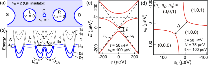
We consider a triple QAD system at Landau-level filling factor in the bulk, as shown in Fig. 1(a). The left (L), central (C), and right (R) QADs are formed with local filling factors, , , and , respectively, between the source (S) and drain (D) regions, where is assumed for a localized state as QAD C in this paper. The following scheme should work even for other filling factors. The energy diagram of the system is schematically shown in Fig. 1(b) for spin-up and -down branches of the lowest and second-lowest Landau levels. Transport is dominated by tunneling through bound states, , , and , in the spin-down lowest Landau level (0). The tunnel coupling, and , and the electrostatic coupling, and , should be determined by the potential profile of the QH insulator. Notice that the bulk is insulating only near the QH filling factor ( in our case). Deviation from the integer value induces occupation of integer charges on localized states randomly distributed in the sample, which alters the potential profile. Therefore, standard techniques, such as surface gates that change the electron density underneath and adjusting magnetic field that changes the flux density, may not provide smooth control of tunnel coupling. Here, we use as a control knob to induce tunnel and electrostatic coupling between QADs L and R by utilizing second-order tunneling.
The hybridization of QADs L, C, and R can be described by the effective one-electron Hamiltonian
| (1) |
for the first electron from the reference electron numbers in the system. Here, we consider only the nearest-neighbor tunneling and by neglecting distant tunneling between L and R. Only a single energy level in each QAD is considered for simplicity. Figure 1(c) shows the eigenenergies of the system as a function of the energy bias for and at and (the solid lines). As compared to the uncoupled case with (the dashed lines), finite energy splitting is seen in the hybridized states (the solid lines) around the crossing of and . The bottom trace shows the ground-state energy of the one-electron system. The splitting at is tunable with even when is fixed. The second-order tunneling can be seen in the approximated form of for .
We study the higher-order tunneling by investigating the charging diagram of the triple QADs. The system accommodates (, , ) numbers of excess electrons in the respective QADs by varying and . In the absence of distant electrostatic coupling between L and R, the two-electron Hamiltonian reads
| (2) |
for the charge bases , , and . The ground-state energy of the two-electron system can be obtained by diagonalizing . The system takes the charge state with minimum energy, as shown in the stability diagram of Fig. 1(d) in the plane. The boundaries among three regions with different total electron number are shown by the red lines. Here, we investigate the minimum spacing between the charge states and in this paper. For and , is given by
| (3) |
which includes . The remainder can be understood as emergent electrostatic coupling induced by the second-order tunneling ( for ). Therefore, observation of finite induced at small suggests tunable coupling of and . Note that symmetric parameters ( and ) are assumed for simplicity, and tunable coupling is expected even with asymmetric parameters.
The model is equivalent to that for triple QDs. While similar three-level systems can be seen in previous studies on QDs and atoms TakakuraAPL2014 ; WaughPRL1995 ; GroveRasmussenNanoLett2008 , their realization in QADs would provide a significant step for coherent control of quasiparticles.
III Experiment
III.1 Sample and measurement setup
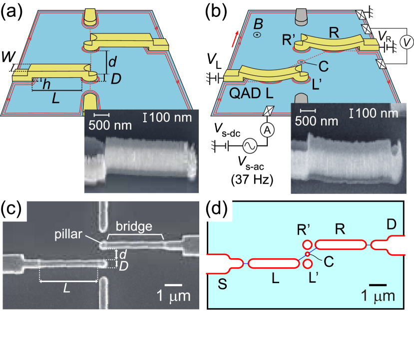
Our sample was fabricated in a standard AlGaAs/GaAs heterostructure with two-dimensional electron gas located at 100 nm below the surface. With an electron density of , a QH state at can be prepared by applying perpendicular magnetic field . Two airbridge gates with Ti (thickness of ) and Au () layers were fabricated by using electron-beam lithography with a triple layer resist EguchiAPEX2019 ; HataJJAP2020 . Each gate has a small pillar of diameter and is connected to the lead electrode through the bridge of length , width , and bridge height , as shown in Fig. 2(a). The two pillars are separated by distance . This device was originally designed to form two QADs around the pillars [the red circles in Fig. 2(a)]. Such airbridge gates worked nicely in our previous paper EguchiAPEX2019 ; HataJJAP2020 . However, for the particular device used in this work, it turned out that the airbridges have been deformed, as shown in Fig. 2(b) with an SEM picture taken after the measurement. The central part of the bridge is touching the surface of the heterostructure. We noticed later that the deformation was introduced during the post photo-lithography process with PMGI, which was not used for the previous devices. Note that the deformation of the bridge is reproducible with the same process, whereas the detailed mechanism of the deformation is not known.
As a result of the deformation, a relatively large QAD with the area of should be formed under the deformed bridge. This area is comparable to those of typical QADs seen in the literature KouPRL2012 . We find that such QADs, referred to as QADs L and R, under the deformed bridges work nicely in this work. However, we did not find any characteristics associated with the intended QADs L’ and R’ under the pillars [see Section III-C].
We take advantage of localized states present in our device. While they are randomly distributed in the sample, we focus on a specific localized state, which acts as QAD C, located between QADs L and R. Following measurements suggests that QAD C with the area of , equivalent to a circle with a diameter of , is located in the middle of QAD L and R, as illustrated in Fig. 2(b) [see Section III-B]. Figure 2(c) shows the top view SEM image of the present device taken after the measurements, where pillars, (deformed) airbridges, and lead electrodes are seen. Schematic locations of QADs are illustrated in Fig. 2(d), while QADs L’ and R’ might be merged into L and R, respectively.
The transport through the QADs is investigated by applying AC voltage at and DC voltage (= 0 unless otherwise noted) to the source and measuring the AC voltage drop between the voltage probes with a lock-in amplifier [Fig. 2(b)]. The differential conductance is estimated from the relation . All measurements were performed in a dilution refrigerator with a base temperature of about .
III.2 Localized state as QAD C
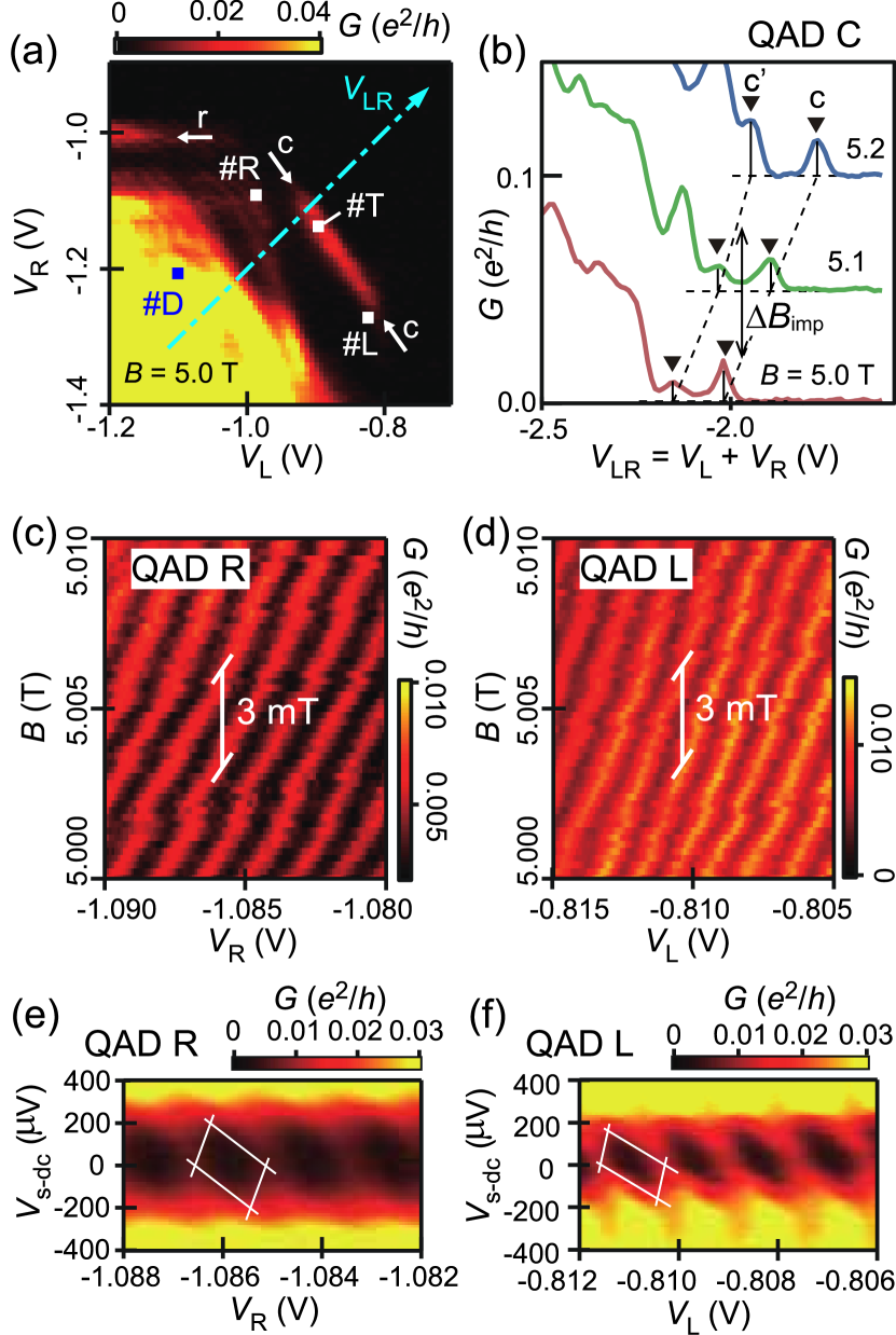
Figure 3(a) shows a color plot of conductance over the wide ranges of and at . Whereas the Coulomb oscillations of QAD L and R are not visible with this coarse scan, several current peaks associated with localized states are resolved. For example, the horizontal line at V (marked by the arrow labeled r) should be associated with a localized state near the right gate with but far from the left gate with . We focus on a specific localized state that exhibits the current peak marked by the arrows labeled c. As this peak is elongated in the lower-right direction with a slope of in the figure, the state is almost equally coupled to the two gates, and thus should be located at around the center of the two gates (slightly closer to the left gate). We shall use this localized state as QAD C in the following.
Figure 3(b) shows the conductance traces taken by simultaneously changing and along the dot–dashed line labeled in Fig. 3(a) for several values. In Fig. 3(b), the two peaks labeled c and c’ evolve in a similar manner with , as shown by the dashed lines, implying that they are two consecutive CB peaks for the same impurity. The corresponding magnetic-field period of about suggests that the area enclosed by the bound state is by assuming local filling factor . If the bound state is circular, its diameter of can fit in between the two gates with the distance of 500 nm, as illustrated in Fig. 2(d).
In Section II-E, we focus on peak c of Fig. 3(b), where rich characteristics associated with QADs L, C, and R show up in the fine sweep of and .
III.3 Single QAD L and R
The QADs L and R were investigated separately by focusing on the conditions #L and #R, respectively, in the plane of Fig. 3(a). The transport is effectively determined by each QAD under the asymmetric gate voltages, where other QADs are strongly coupled to the leads. CB oscillations of QAD R can be seen in fine sweeps of and , as shown in Fig. 3(c). Its oscillation period in is 3 mT, which corresponds to the area enclosed by the bound states, 0.7 (m)2. Here, the factor is used for the two occupied spin-resolved Landau levels with , where bound states associated with the two Landau levels strongly interacted electrostatically HwangPRB1991 ; FordPRB1994 ; KataokaPRL1999 ; SimPhysRep2007 . This is comparable to the area of the deformed bridge [] but far from the area of the pillar [)] in consistency with QAD R being formed under the deformed gate.
The Coulomb diamond characteristics of QAD R are obtained by applying and , as shown in Fig. 3(e). The CB region with is seen in the voltage range 200 , as illustrated by a white parallelogram as a guide. This measures the addition energy 200 , which includes the on-site Coulomb charging energy and level spacing of the bound states. This value is comparable to typical values of reported QADs with similar sizes KouPRL2012 . The energy of each bound state can be shifted by with small change in , where the lever arm factor is roughly estimated from the size of the parallelogram.
Similarly, QAD L investigated at around condition #L shows CB oscillations in Fig. 3(d). The oscillation period 3 mT also suggests that the QAD is formed under the deformed bridge. The two QADs show similar oscillation periods in as well as their gate voltages ( and ). The Coulomb diamond characteristics for QAD L in Fig. 3(f) show smaller blockade regions with somewhat smaller addition energy 180 and . Similar QADs with small differences are well reproduced by the deformed bridges.
III.4 Uncoupled double QAD
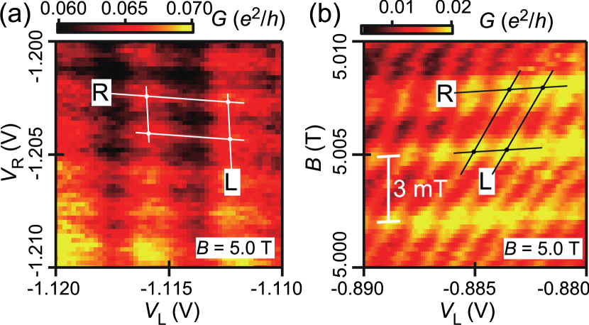
Transport through QADs L and R with a negligible role of QAD C can be seen when large negative voltages, and , are applied. Figure 4(a) shows such Coulomb oscillations in the fine sweep of and at around condition #D in Fig. 3(a). The oscillations for QAD L (the vertical lines) and R (the horizontal lines) are resolved but not influenced by each other with no measurable splitting at their crossings, as shown by the white parallelogram in Fig. 4(a). This is the signature of negligible tunnel and electrostatic couplings, as studied with conventional QDs WielRevModPhys2003 .
Another example of uncoupled QADs is shown in the plane of Fig. 4(b), where the parallelogram pattern (the black lines) for CB oscillations of QAD L and R is resolved. Whereas this and range is the condition where triple QAD formation is expected [#T in Fig. 3(a)], a negligible role of QAD C is seen probably due to small tunneling (, ) in this range. The magnetic field periods, 3 mT and 3 mT, are similar to those obtained for single QADs. Therefore, QADs L and R are stably formed in the wide range of and .
The above data show that distant QADs L and R are uncoupled with negligible tunneling () and electrostatic () couplings. However, the two QADs can be coupled by introducing QAD C, as shown in the next subsection.
III.5 Triple QAD
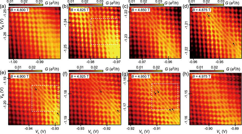
Coupling of QADs L, C, and R can be found in Fig. 5, where was measured with a fine sweep of and at various magnetic fields. The sweep ranges of and are adjusted for each to keep the focus on the resonance with QAD C [the equivalent condition is marked by #T in Fig. 3(a)]. Fine oscillations are superimposed on the broad peak of QAD C. Rich characteristics ranging from parallelogram to honeycomb patterns are seen. In addition, sharp diagonal lines (some marked by the arrows) show up in the limited range of 4.875 T 4.950 T. Some representative characteristics are analyzed in the following.
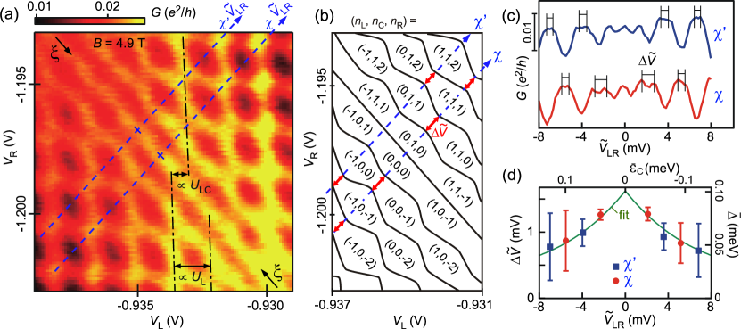
First, we focus on the white dashed region of Fig. 5(e) at 4.900 T, which is enlarged in Fig. 6(a). Strikingly, one of the CB peaks follows the single straight diagonal line between the two arrows labeled . This line is located around the center of the CB peak of QAD C, and the line width is much sharper than the peak width of QAD C. The meaning of the diagonal line is clarified by analyzing the Coulomb oscillations of QADs L and R. The CB peaks of QAD L [the dot-dashed lines in Fig. 6(a)] are abruptly shifted across the diagonal line. This shift suggests that the charge state of QAD C is changed from (the lower-left side) to (the upper-right side), which influences the potential of QAD L. Therefore, we define on the diagonal line. The shift measures the electrostatic coupling between QAD L and C. Similar shift is seen for CB peaks of QAD R (not marked), from which is estimated. It should be noted that the straight diagonal line is associated with a special resonance of hybridized states under symmetric conditions of the triple QAD, as elaborated in Section IV.
The current profile in the vicinity of the diagonal line shows a clear rounded honeycomb pattern, which manifests finite coupling between QAD L and R. The honeycomb pattern gradually changes to the parallelogram pattern toward the upper-right and lower-left corners. The corresponding charge stability diagram is sketched in Fig. 6(b), where each region is labeled with excess electron numbers from a reference. We investigate the minimum spacing between the rounded charge boundaries, which corresponds to in Eq. (3). The overall conductance profile is mirror symmetric about the diagonal line and periodic along the diagonal line (the upper-left direction). This feature suggests that the spacing is dominantly changed only by , i.e. the distance from the diagonal line. Other parameters, specifically and , are unchanged within the sweep range of and . Otherwise, the conductance pattern should change in a non-symmetric way. These characteristics support the demonstration of tunable coupling with cotunneling.
Cross-sectional current profiles passing through several anticrossing conditions are shown in Fig. 6(c). Here, two cross sections and pick up different anticrossings as illustrated by the dashed lines in Figs. 6(a) and (b). The axis denotes the relative gate voltage in measured from the central diagonal line (). The splitting is shown by the bars in Fig. 6(c). The precise values and their errors are determined from the overall pattern in Fig. 6(a). For example, the peak (spot) slightly elongated to the upper-right direction suggests finite splitting, even if the two split peaks are unresolved in the cross-sectional plot. The estimated is plotted as a function of in Fig. 6(d), in which the symmetric variation of is seen.
can be converted into the splitting energy, , by using the lever arm factor [See Appendix A], as shown in the right scale. To see the consistency with the proposed scheme, we assume equal tunnel coupling (), which will be justified in Section IV-A, and linear dependence of on with unknown factor . Here, symbols with a bar ( and ) denote the quantities obtained for different charge states, while the original and are defined for a given charge state. We apply Eq. (3) by replacing and with and for the fitting to the data. By using , the measured is well reproduced by the fitting [the solid green line in Fig. 6(d)] with adjusted parameters, and . Here, tuning of is induced by the purely capacitive effect with but partially compensated by the excess charge of the QADs ( and ). They are related by , where is defined for the region at [see Fig. 6(b)]. We obtained from the relations. This does not contradict the realistic lever-arm factors in our sample [See Appendix A], and supports our scheme. Therefore, the result indicates that the total coupling energy , as well as the tunnel coupling , are successfully controlled with the energy of the localized state in the range of ( in the present case).
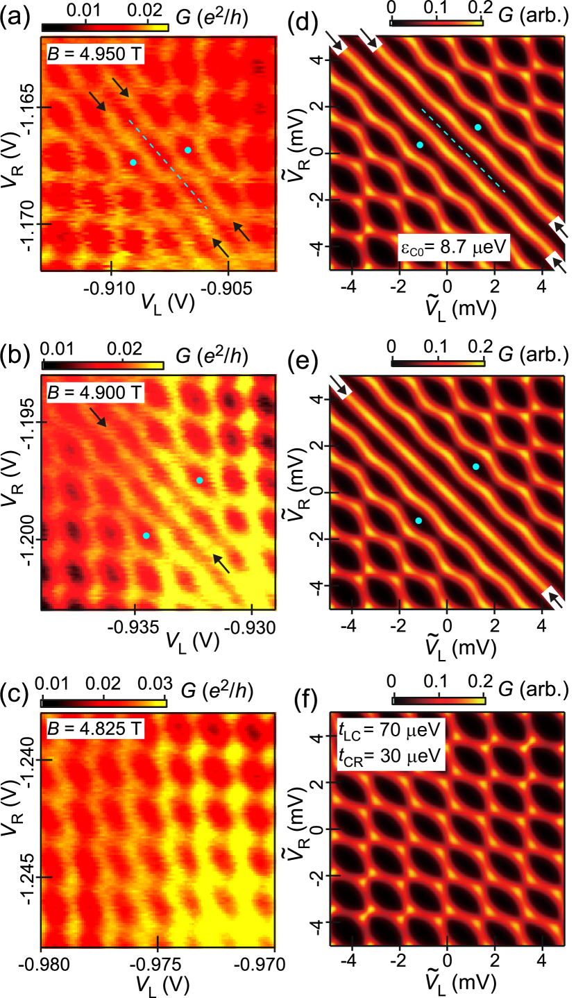
The tunable tunnel coupling can be confirmed in the wide range of , as shown in Fig. 5. In all cases, one can see honeycomb patterns near the center of the CB peak of QAD C and parallelogram patterns near the upper-right and lower-left corners. However, the precise patterns including the diagonal lines near the CB peak of QAD C change significantly with . The white dashed regions in Figs. 5(b), (e), and (g) are magnified in Figs. 7(b), (c), and (a), respectively. Two diagonal lines (indicated by the arrows) are resolved at in Fig. 7(a), whereas only a single line is seen at in Fig. 7(b) [the same data as Fig. 6(a)]. No clear diagonal line is resolved at in Fig. 7(c) [see also and in Figs. 5(a) and (h), respectively], while the honeycomb pattern with finite splitting is seen. Full understanding requires detailed analysis on the symmetry of the QAD parameters, as shown in the next section.
IV Symmetry of triple QAD
IV.1 System Hamiltonian
First of all, we should note the differences in electronic states between QADs and standard QDs. For QDs at zero or low magnetic fields, the energy levels are strongly influenced by many-body effects with direct and exchange interactions as well as single-particle orbitals and Zeeman splittings. As a result, CB oscillations are generally aperiodic and thus charge stability diagrams of multiple QDs are complicated with many jumps in the CB conditions TakakuraAPL2014 ; WaughPRL1995 ; GaudreauPRL2006 ; SchroerPRB2007 ; GroveRasmussenNanoLett2008 ; TakakuraAPL2010 ; BuslNatNano2013 ; BraakmanNatNano2013 ; NoiriPRB2017 ; WangNanoLetters2017 In contrast, the energy quantization of QADs in the integer QH system is dominated by the Aharonov-Bohm effect, which determines the area of the bound state under uniform . Therefore, the energy spacing is almost constant for a smooth QAD potential for each spin-resolved Landau level. When multiple Landau levels are involved for each QAD, occupation of the inner Landau level is well screened by the outer one. Therefore, CB oscillations are periodic with a constant addition energy for different charge states KataokaPRB2000 . The deviation from the periodic pattern is studied with the hybridization of the system, as shown below.
In this paper, a symmetric QAD with and is assumed for proposing the tunable second-order coupling scheme. While the symmetry is not required just for tuning the tunnel coupling, we should investigate the role of the symmetry in the hybridization. Interestingly, we found that the diagonal straight line observed in Fig. 6(a) is the signature of the symmetry.
Generally, CB peaks appear when the ground-state energy of the -electron system coincides with that of the -electron system, where the electrochemical potential of the system equals the chemical potentials (defined to be zero) of the leads. The appearance of the diagonal straight line suggests that this equality () is satisfied on the diagonal line over several charge states. In the presence of significant nearest-neighbor tunneling (), the most probable situation is that the - and -electron systems share the identical eigenenergies including the ground-state one with the same form of Hamiltonians and .
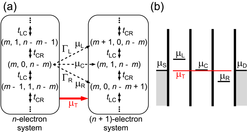
To see this happens, the excess charges (, , ) that belong to the - and -electron systems are listed in Fig. 8(a) with an integer in such a way that electrons are moved from the left to the right by tunneling processes with and under the constraint . The total energy of state in the absence of tunneling can be written as
Therefore, the matrix form of the Hamiltonian with charge bases has diagonal elements of and nearest-neighbor off-diagonal elements and . and in Eqs. (1) and (2) are examples of and in the reduced Hilbert space (only for three charge states). The conditions for identical Hamiltonians () are , (), (), , and . The straight diagonal line is expected to appear if all conditions are met.
The last two conditions can be written with convenient but misleading electrochemical potentials , , and for adding an electron to QADs L, C, and R, respectively, from charge state [the dashed arrows in Fig. 8(a)], where the hybridization is not considered at all. Notice under the required conditions, as shown in the energy diagram of Fig. 8(b). Conventional sequential-tunneling transport is not allowed for this condition (), and thus does not explain the appearance of the diagonal line. In the presence of significant , the charge states of - and -electron systems are strongly hybridized with the identical matrix form of Hamiltonians, and thus the correct electrochemical potential of the triple QAD is on the diagonal line. Therefore, the hybridization plays an essential role in the appearance of the diagonal line.
The appearance of the diagonal line implies that the system satisfies all conditions. As our sample shows and , and must be satisfied within the experimental allowance. Considering the variations of the patterns at different ’s in Fig. 5, the data in Fig. 6(a) could be the special case close to the symmetric conditions.
IV.2 Numerical simulation
The current profiles under the symmetric and non-symmetric conditions are calculated by using the standard master equation FujisawaPhysicaE2011 . The two gate voltages, and , control the electrostatic potentials of the three QADs, , , and , with the lever arm factors, , , and , and offset energies and [see Appendix A for their definitions]. The Hamiltonian is diagonalized to obtain the eigenstates. The current through the triple QAD is calculated for small bias voltage between the source and the drain at electron temperature (). Tunneling rates to the source and the drain are fixed at 1 GHz. The calculation scheme for the wide range of charge states is described in Appendix B.
Figure 7(e) shows the calculated under the symmetric condition with , , and , where identical Hamiltonian is expected at . The central diagonal line (marked by the arrows) is reproduced at . The honeycomb pattern is clearly resolved near the line, and the splitting is gradually decreasing toward the upper-right and lower-left corners. All features are symmetric about the diagonal line (highlighted by the dot pair). They are qualitatively the same as the experimental features including the mirror symmetry in Fig. 7(b), which suggests that the symmetric conditions are satisfied in the experiment.
When a small energy offset of 8.7 eV is introduced to the conditions for Fig. 7(e), the pattern is no longer mirror symmetric about the diagonal line, as shown in Fig. 7(d). The pattern shows the glide reflection symmetry (highlighted by the dot pair) about the dashed line between the double diagonal line (marked by the arrows). Such glide reflection symmetry is seen in our experimental data of Fig. 7(a).
Identical tunneling with is the essential condition. Our simulation (not shown) suggests that we would not recognize the deviation from the straight diagonal line if the asymmetry is not large (). When large ( and ) is assumed in the simulation, the diagonal line disappears as shown in Fig. 7(f). While the honeycomb pattern is seen in the entire region of the figure, the splitting shows gentle variation. Similar pattern is seen in our data of Fig. 7(c), whereas the parameters for Fig. 7(f) were not adjusted to the experimental data.
Identical Coulomb interactions with and are important for the periodicity along the diagonal line. Some diagonal lines are visible only for a few oscillation periods, which may be related to small asymmetry in the Coulomb interactions.
Whereas we observed smooth tuning of honeycomb patterns with gate voltages, we do not see systematic variation with the magnetic field. Slight change in magnetic field can induce drastic change in the stability diagram, which might be related to uncontrollable charging of localized states.
V Summary
We have proposed and demonstrated the triple QAD scheme for tunable coupling between two separate QADs by using cotunneling through the central QAD. The charge stability diagram of the system changes from the parallelogram pattern for the uncoupled case to the round honeycomb pattern for the coupled case by tuning the energy level of the central QAD. In a special case, the charge diagram shows diagonal straight lines as a signature of symmetric parameters of the triple QAD. Systematic variation of transport characteristics are studied by numerical calculation based on the master equation and by experiment with unintentional QADs and a localized state. The system can be made more tunable, if the localized state is replaced by an intentional QAD with an independent gate. Our research has paved the way for further studies on multiple QADs in the integer and fractional QH states, such as a QAD array for anyon operations AverinPhysicaE2007 .
Acknowledgement
This work was supported by JSPS KAKENHI Grant No. JP19H05603 and JP19K14630, and partially conducted at Nanofab in the Tokyo Institute of Technology supported by “Advanced Research Infrastructure for Materials and Nanotechnology (ARIM)” in Japan and at Materials Analysis Division, Open Facility Center in Tokyo Institute of Technology.
Appendix A Lever arm factors
The electrostatic potentials , , and can be changed by the gate voltages and with linear relations,
| (5) | |||||
with lever arm factors (’s) and offsets ( and so on). We estimated from the data in Fig. 3(e) and from Fig. 3(f). The CB oscillation periods of QAD L and R in Fig. 6(a) at #T are similar and close to the period of QAD R at #R. Therefore, the lever arm factor was used to obtain in Fig. 6(d). The small ratios are estimated from the slope of the CB oscillations (the dot-dashed lines for ) in Fig. 6(a), but and are neglected in the numerical calculations for simplicity.
Unfortunately, we have no direct estimates on and . For example, describing the effect of the left gate on the QAD C potential should arise from the direct capacitive coupling and indirect coupling through QAD L. Whereas the former contribution is unknown, the latter can be estimated from . As should be smaller than , as well as should be in the range of . If available, these values provide for the determination in Fig. 6(d). This parameter range does not contradict obtained from the fitting to the data in Fig. 6(d). Therefore, we used in the numerical simulations.
Appendix B Calculation of triple-QAD current
We calculated the current through the triple QAD based on the master equation FujisawaPhysicaE2011 . The electrochemical potential for the first excess electron only in QAD can be controlled with excess gate voltages and , in the form of Eq. (5). Here, plays an important role in the stability diagram, and we set and for simplicity. The Hamiltonian shown in Sec. IV-A is diagonalized to obtain -th eigenenergy of -electron system. Transport through the triple QAD can be calculated by considering tunnel transitions to the leads. We assumed energy-independent tunneling rates between the source and QAD L and between QAD R and the drain. A master equation for occupation probabilities of the eigenstates is constructed under a small bias voltage 30 V and thermal energy 10 V in the leads. For each and , a few eigenstates with energies in the range of contribute to the transport, where is the total ground-state energy for all possible and . The eigenstates within this energy range are considered in solving the master equation. The current was calculated from the steady-state occupation probabilities.
References
- (1) Sivan, I. et al. Observation of interaction-induced modulations of a quantum Hall liquid’s area. Nature Communications 7, 1–9 (2016).
- (2) Röösli, M. P. et al. Observation of quantum hall interferometer phase jumps due to a change in the number of bulk quasiparticles. Phys. Rev. B 101, 125302 (2020).
- (3) Röösli, M. P. et al. Fractional coulomb blockade for quasi-particle tunneling between edge channels. Science Advances 7, eabf5547 (2021).
- (4) Hwang, S. W., Simmons, J. A., Tsui, D. C. & Shayegan, M. Quantum interference in two independently tunable parallel point contacts. Phys. Rev. B 44, 13497–13503 (1991).
- (5) Ford, C. J. B. et al. Charging and double-frequency aharonov-bohm effects in an open system. Phys. Rev. B 49, 17456–17459 (1994).
- (6) Kataoka, M. et al. Detection of coulomb charging around an antidot in the quantum hall regime. Phys. Rev. Lett. 83, 160–163 (1999).
- (7) Sim, H.-S., Kataoka, M. & Ford, C. Electron interactions in an antidot in the integer quantum hall regime. Physics Reports 456, 127–165 (2008).
- (8) Mills, S. M. et al. Dirac fermion quantum hall antidot in graphene. Phys. Rev. B 100, 245130 (2019).
- (9) Mills, S. M., Averin, D. V. & Du, X. Localizing fractional quasiparticles on graphene quantum hall antidots. Phys. Rev. Lett. 125, 227701 (2020).
- (10) Halperin, B. I., Stern, A., Neder, I. & Rosenow, B. Theory of the fabry-pérot quantum hall interferometer. Phys. Rev. B 83, 155440 (2011).
- (11) Rosenow, B. & Stern, A. Flux superperiods and periodicity transitions in quantum hall interferometers. Phys. Rev. Lett. 124, 106805 (2020).
- (12) Nakamura, J. et al. Aharonov-Bohm interference of fractional quantum Hall edge modes. Nature Physics (2019).
- (13) Nakamura, J., Liang, S., Gardner, G. C. & Manfra, M. J. Direct observation of anyonic braiding statistics. Nature Physics 16, 931–936 (2020).
- (14) Averin, D. V. & Nesteroff, J. A. Correlated transport of FQHE quasiparticles in a double-antidot system. Physica E: Low-Dimensional Systems and Nanostructures 40, 58–66 (2007).
- (15) van der Wiel, W. G. et al. Electron transport through double quantum dots. Rev. Mod. Phys. 75, 1–22 (2002).
- (16) Hayashi, T., Fujisawa, T., Cheong, H. D., Jeong, Y. H. & Hirayama, Y. Coherent manipulation of electronic states in a double quantum dot. Phys. Rev. Lett. 91, 226804 (2003).
- (17) Petta, J. R. et al. Coherent manipulation of coupled electron spins in semiconductor quantum dots. Science 309, 2180–2184 (2005).
- (18) Gould, C., Sachrajda, A. S., Dharma-wardana, M. W. C., Feng, Y. & Coleridge, P. T. “spectator” modes and antidot molecules. Phys. Rev. Lett. 77, 5272–5275 (1996).
- (19) Maasilta, I. J. & Goldman, V. J. Tunneling through a coherent “quantum antidot molecule”. Phys. Rev. Lett. 84, 1776–1779 (2000).
- (20) Ezawa, Z. F. Quantum Hall Effects: Recent Theoretical and Experimental Developments (World Scientific Publishing Company, 2013).
- (21) Takakura, T. et al. Single to quadruple quantum dots with tunable tunnel couplings. Applied Physics Letters 104, 113109 (2014).
- (22) Waugh, F. R. et al. Single-electron charging in double and triple quantum dots with tunable coupling. Phys. Rev. Lett. 75, 705–708 (1995).
- (23) Grove-Rasmussen, K., Jørgensen, H. I., Hayashi, T., Lindelof, P. E. & Fujisawa, T. A triple quantum dot in a single-wall carbon nanotube. Nano Letters 8, 1055–1060 (2008).
- (24) Eguchi, R., Kamata, E., Lin, C., Aramaki, H. & Fujisawa, T. Quantum anti-dot formed with an airbridge gate in the quantum hall regime. Applied Physics Express 12, 065002 (2019).
- (25) Hata, T., Uchino, T., Akiho, T., Muraki, K. & Fujisawa, T. Sensitive current measurement on a quantum antidot with a corbino-type electrode. Japanese Journal of Applied Physics 59, SGGI03 (2020).
- (26) Kou, A., Marcus, C. M., Pfeiffer, L. N. & West, K. W. Coulomb oscillations in antidots in the integer and fractional quantum hall regimes. Phys. Rev. Lett. 108, 256803 (2012).
- (27) Gaudreau, L. et al. Stability diagram of a few-electron triple dot. Phys. Rev. Lett. 97, 036807 (2006).
- (28) Schröer, D. et al. Electrostatically defined serial triple quantum dot charged with few electrons. Phys. Rev. B 76, 075306 (2007).
- (29) Takakura, T. et al. Triple quantum dot device designed for three spin qubits. Applied Physics Letters 97, 212104 (2010).
- (30) Busl, M. et al. Bipolar spin blockade and coherent state superpositions in a triple quantum dot. Nature Nanotechnology 8, 261–265 (2013).
- (31) Braakman, F. R., Barthelemy, P., Reichl, C., Wegscheider, W. & Vandersypen, L. M. Long-distance coherent coupling in a quantum dot array. Nature Nanotechnology 8, 432–437 (2013).
- (32) Noiri, A. et al. Cotunneling spin blockade observed in a three-terminal triple quantum dot. Phys. Rev. B 96, 155414 (2017).
- (33) Wang, J.-Y. et al. Coherent transport in a linear triple quantum dot made from a pure-phase inas nanowire. Nano Letters 17, 4158–4164 (2017).
- (34) Kataoka, M. et al. Coulomb blockade of tunneling through compressible rings formed around an antidot: An explanation for aharonov-bohm oscillations. Phys. Rev. B 62, R4817–R4820 (2000).
- (35) Fujisawa, T., Shinkai, G., Hayashi, T. & Ota, T. Multiple two-qubit operations for a coupled semiconductor charge qubit. Physica E: Low-dimensional Systems and Nanostructures 43, 730–734 (2011).