Multi-level Operation of FeFETs Memristors:
the Crucial Role of Three Dimensional Effects
Abstract
This paper investigates and compares through a comprehensive TCAD analysis 2D and 3D simulations for ferroelectric based FETs. We provide clear evidence that the multiple read conductance values experimentally observed in FeFETs stem from source to drain percolation current paths, which are governed by the polarization patterns in the ferroelectric domains. Such a physical picture makes 3D simulations indispensable to capture even the qualitative features of the device behaviour, not to mention the quantitative aspects.
© 2023 IEEE. Personal use of this material is permitted. Permission from IEEE must be obtained for all other uses, in any current or future media, including reprinting/republishing this material for advertising or promotional purposes, creating new collective works, for resale or redistribution to servers or lists, or reuse of any copyrighted component of this work in other works.
https://ieeexplore.ieee.org/document/9947169
1 Introduction
Ferroelectric based FETs (FeFETs) are very promising memories and memristors for neuromorphic computing [2, 1]. Unlike other device concepts, such as resistive RAMs (ReRAM) or Phase Change Memories (PCM) [3], that require a current flow for the switching operation, the physical substrate offered by FeFETs exploits a displacement current to set the ferroelectric polarization, thus holding the promise of low-power consumption memristors [4].
Ferroelectric oxides for CMOS compabile devices are based either on hafnium oxides with Si doping (HSO) or on hafnium zirconium oxides (HZO), both exhibiting remnant polarization values ranging from 15 to 30 C/cm2 and coercive fields in the range of 1-2 MV/cm [5, 6, 7, 8].
It is well known that ferroelectric materials tend to minimize their free energy by creating domains [10, 9], whose size is usually associated to the size of the polycrystalline grains [11]. Indeed, for the film thicknesses of practical interest for nanoscaled electronic devices, namely in the range of 5-10 nm, ferroelectric oxides are polycristalline with a grain size in the nanometer range [11, 12].
In this paper, a physical based TCAD simulation approach is used to account for the multi-domain nature of the ferroelectric material and thus explore a multi-level operation of FeFETs memristors.
2 Modelling of the FeFET
Simulations are carried out by using the TCAD tool Sentaurus-Device package [13], that couples the drift-diffusion equations with a kinetic model for the ferroelectric dynamics based on the phenomenological Landau-Ginzburg-Devonshire (LGD) equation [13].
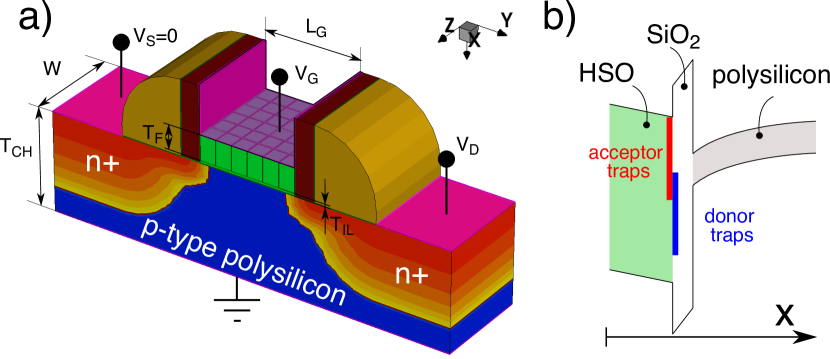
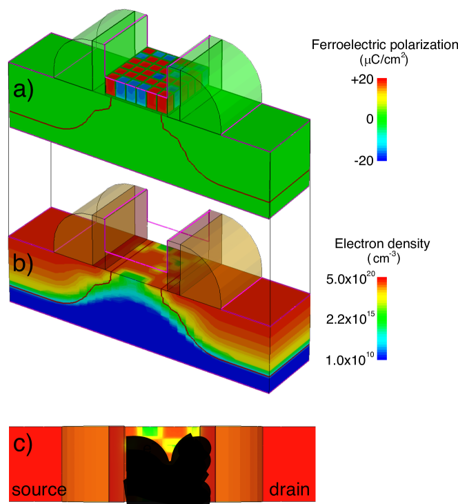
A sketch of the simulated device is shown in Fig.1, where the polycristalline nature of the ferroelectric HfO2 is described by defining square ferroelectric domains having a 6 nm size in the - plane, namely in the range of experimentally reported values [11, 12]. An essentially uniform polarization inside each grain is enforced by using an artificially large value of the domain wall coupling parameter [13]. Ferroelectric domains are separated by a thin non-ferroelectric spacer having the same dielectric constant as HSO (i.e. =30 [14]). The electrostatic coupling between the domains is inherently accounted for in simulations. However the model does not assign any energy penalty to the formation of domains with an anti-parallel polarization or, equivalently, to the formation of 180° domain walls. This is consistent with recent ab-initio calculations of the domain wall energy in HfO2 based ferroelectrics [15].
The calibration of the Landau’s anysotropic constants has been previously carried out by comparison against experimental data for an HSO capacitor [16], leading to = m/F, = m5/(FC2), = m9/(FC4), corresponding to a remnant polarization PR20 Ccm2 and a coercive field EC1.1 MVcm. Our simulations include a domain to domain statistical dispersion of the ferroelectric properties by using a normal distribution for the coercive electric field featuring a mean value EC1.1 MVcm and a standard deviation =0.3EC,0. The resistivity for the ferroelectric switching employed in simulations is =110 m [17], resulting in a time constant =/2100 ns.
In this work we consider a channel length of 40 nm, corresponding to six ferroelectric domains in the source to drain direction. Furthermore, we denote as 2D simulations those including a single domain in the device width direction (i.e. 61 FeFET), and as 3D simulations those featuring more domains in the transverse direction (e.g. 63 and 66 FeFETs). Between the ferroelectric oxide and the polysilicon channel, which is compatible with a BEOL integration, the simulated FeFET has a 1 nm thick SiO2 interlayer (IL), which is typically observed in conventional growth processes for hafnia-based ferroelectrics on silicon [18, 5]. This layer plays an important role in the modelling of the device in several respects. Indeed, experimental results based on Hall and split-CV measurements suggest that most of the charge compensating for the ferroelectric polarization is located in the IL at the ferroelectric-dielectric interface [19], as it’s been also confirmed in more recent experiments and simulations [8]. Moreover, in the absence of traps, the voltage drop across the IL reduces the drop on the ferroeletric and can lead to the so called minor-loop operation, where domains with trajectories located along nonsaturated hysteresis loops tend to back-switch after the write programming phase. Indeed, we have previously shown that, by neglecting altogether the charge trapping, simulations exhibit irreconcilable discrepancies with the experimental results [16]. Based on these premises, in the simulations of this work we employed an interfacial trap density at the FE-IL interface as reported in Fig. 1b. Interfacial traps in this work can exchange carriers with the polysilicon channel through a non-local trapping model that includes both elastic and phonon-mediated tunneling processses across the SiO2 IL [13]. Tunneling emission and capture rates are described by the trap volume, the Huang-Rhys factor, the phonon energy and the tunneling masses [13], which can be regarded as fitting parameters and for the SiO2 IL are taken from Ref. [20].
Simulations are performed by using a constant carrier mobility of 10 cm2/Vs in the polysilicon channel [21]. The in this work is 50 mV, therefore the longitudinal electric fields are such that velocity saturation effects are negligible.
In these simulations, the bottom of the polysilicon channel is connected to ground to effectively provide majority carriers (holes) that allow for a positive to negative polarization switching within tens or hundred of nanoseconds. This simulation setup can still represent a BEOL compatible FeFET with the channel lying on a thick oxide layer and that is electrically contacted from the top side.
3 Simulation results
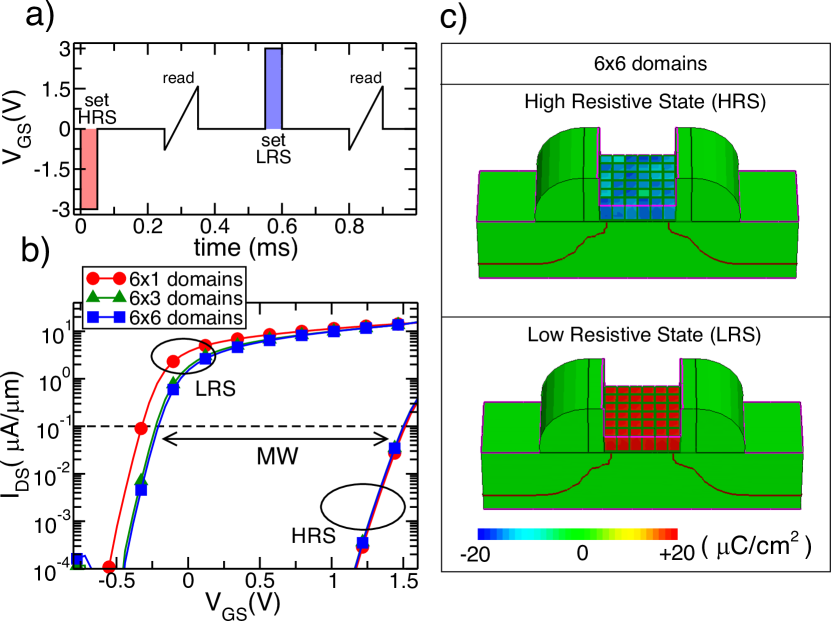
To investigate the maximum shift of the threshold voltage (), or equivalently the memory window (MW) of simulated FeFETs, we first used a positive and negative gate voltage with sufficient amplitude and duration to drive the device in the low resistance (LRS) and high resistance state (HRS), where all the domains have respectively positive or negative polarization111The polarization is defined positive when it points to the transistor channel, namely along the direction in Fig.1.. Figure 2a shows the applied gate voltage scheme, consisting of a write pulse followed by a ramp for the readout (with a read voltage small enough to leave the polarization pattern unperturbed). The versus characteristics are shown in Fig. 2b for a 6x1, a 6x3 and a 6x6 domains FeFET. In the three devices the MW is essentially the same and equal to approximately 1.7 V. Hence, the uniform polarization state enforced by the write pulse makes the device behaviour insensitive to the number of domains in the width direction. Such a simulated MW is in good agreement with the experimental values for the HSO based FeFETs reported in Refs. [22, 11].
In order to explore with simulations the possibility of setting multiple values, we applied a series of increasing number of constant amplitude pulses at the gate terminal followed by a read sweep, as illustrated by the waveforms in Fig. 3. The idea behind this pulse scheme is to exploit the accumulative switching behaviour, where multiple pulses separated by a time delay, tdelay, can induce a progressive polarization switching involving very few and possibly even a single domain [1, 6].
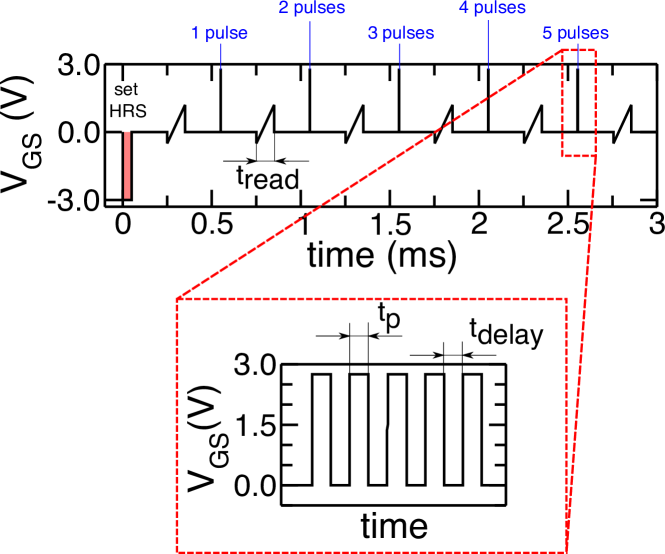
Figure 4 shows the polarization trajectories of each domain (dashed, coloured lines) for the 61 FeFET. The negative to positive switching of polarization in one or a few domains occurs almost at each group of pulses, whereas the read operation does not perturb the stored polarization.
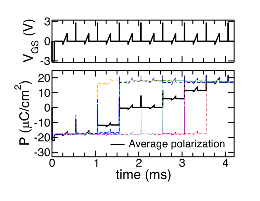
Figure 5 shows the versus curves obtained during the ramp used for the readout operation (see Fig.3). The FeFET with a single domain along the width direction (i.e. the 61 FeFET shown in Fig. 5a) exhibits a digital behaviour. This is because any domain with negative polarization precludes the formation of a source to drain conduction path. Therefore the FeFET is basically in the LRS when all domains have a positive polarization, and it is in the HRS for all other polarization patterns. On the other hand, FeFETs having 3 and 6 domains along the device width exhibit several intermediate values or, equivalently, intermediate current levels in the readout mode. In order to illustrate the physics behind this multi level behaviour, Fig. 6a shows the polarization pattern for the 66 domains FeFET after 15 potentiation pulses. From the electron density map distribution in Fig. 6b-c it can be observed the formation of high conductance paths from source to drain. The number of these conductance paths enlarges by increasing the number of potentiation pulses, which results in the multi-level operation observed in Fig. 5b-c.
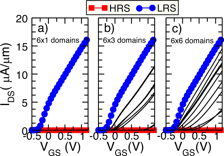
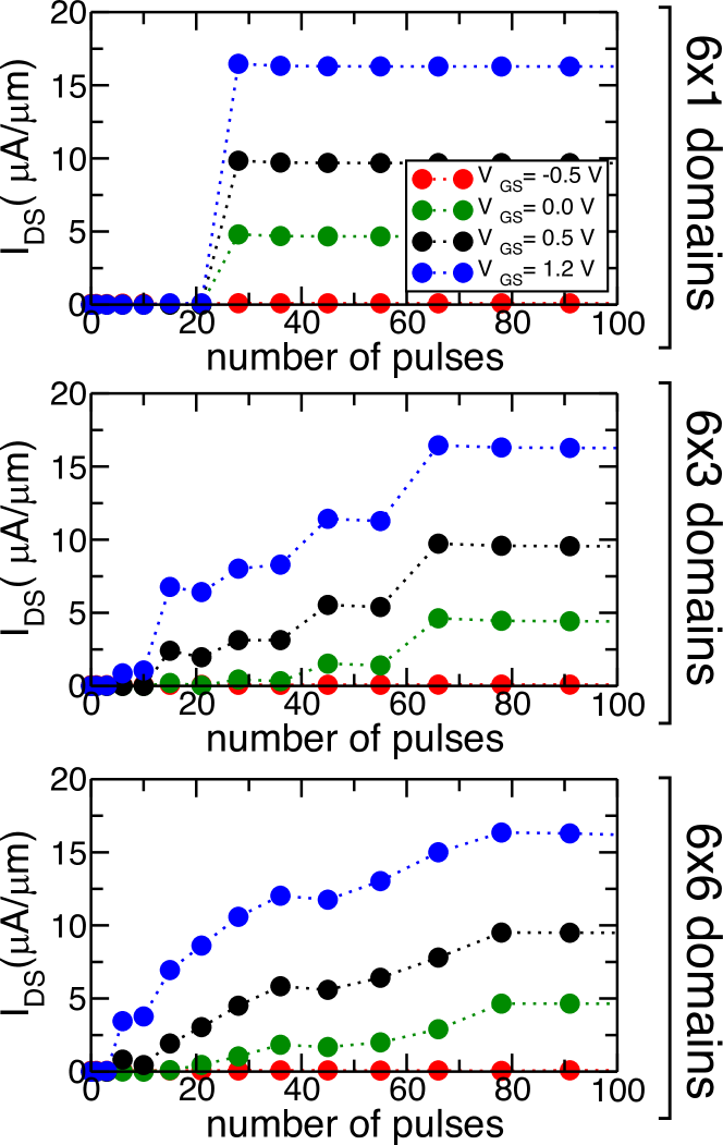
The read current corresponding to different read values is illustrated in Fig. 7 versus the number of potentiation pulses and for the different simulated structures. Consistently with the results shown in Fig. 5, only a single LRS is observed for the 61 FeFET for any read , which is reached after 28 potentiation pulses that set all the ferroelectric domains to a positive polarization. The 63 FeFET exhibits instead a multi-level behaviour, where discrete read values are observed by increasing the number of pulses (and for a fixed read ), corresponding to the activation of new percolation current paths or the reinforcement of existing ones. Hence the read current in the 63 FeFET shows some discrete values which are modulated by the potentiation pulses. Finally, Fig. 7 shows that the 66 FeFET offers an almost continuous set of read values, in virtue of the much larger number of possible source to drain percolation current paths. Consistently with the results in Fig. 5, the three FeFETs have essentially the same read per unit width in the LRS.
4 Discussion and conclusions
This work has presented a comprehensive TCAD study of the multi-level operation in FeFETs memristors, focusing in particular on the difference between 2D and 3D simulations. We found that, if an accumulative switching behavior can be induced in the HSO film, then the modulation of the percolation current paths in the device offers a powerful pathway for a multi-level memristor operation.
Despite the encouraging results in Fig. 7, it should be noticed that the displayed behaviour depends critically on a number of simulation parameters, including the density of traps and their emission and capture rates, as well as the features of the waveforms including the delay times between the groups of potentiation pulses. In our simulations, for instance, the accumulative switching behavior is linked to the trapping dynamics, and it is understood that the properties of traps cannot be regarded as a design knob. Nevertheless, trap densities can be partly engineered in ALD deposited Al2O3 films by tuning the deposition parameters, such as temperature, oxidant precursor type and dosing time [23].
Although the material and device engineering for FeFETs memristors is still a challenging path, our simulations predict good potentials for this class of ferroelectric devices.
Acknowledgments This work was supported by the European Union through the BeFerroSynaptic project (GA:871737).
References
- [1] E. Covi, H. Mulaosmanovic, B. Max, S. Slesazeck and T. Mikolajick, ”Ferroelectric-based synapses and neurons for neuromorphic computing”, Neuromorphic Computing and Engineering, vol. 2, no. 1, 2022.
- [2] S. Slesazeck and T. Mikolajick, ”Nanoscale resistive switching memory devices: a review”, Nanotechnology, vol. 30, no. 35, 2019.
- [3] F. Zahoor, T. Z. Azni Zulkifli and F. A. Khanday, ”Resistive Random Access Memory (RRAM): an Overview of Materials, Switching Mechanism, Performance, Multilevel Cell (mlc) Storage, Modeling, and Applications”, Nanoscale Res. Lett., vol. 15, no. 90, 2020.
- [4] S. Majumdar ”Back-End CMOS Compatible and Flexible Ferroelectric Memories for Neuromorphic Computing and Adaptive Sensing”, Adv. Intell. Syst., pp. 2100175, 2021.
- [5] M. Trentzsch, S. Flachowsky, R. Richter, J. Paul, B. Reimer, D. Utess et al., ”A 28nm HKMG super low power embedded NVM technology based on ferroelectric FETs”, Proceed. of IEDM, pp. 11.5.1-11.5.4, 2016.
- [6] M. Jerry, P.-Y. Chen, J. Zhang, P. Sharma, K. Ni, S. Yu and S. Datta, ”Ferroelectric FET analog synapse for acceleration of deep neural network training”, Proceed. of IEDM, pp. 6.2.1-6.2.4, 2017.
- [7] B. S. Kim, S. D. Hyun, T. Moon, K. D. Kim, Y. H. Lee, H. W. Park et al., ”A Comparative Study on the Ferroelectric Performances in Atomic Layer Deposited Hf0.5Zr0.5O2 Thin Films Using Tetrakis(ethylmethylamino) and Tetrakis(dimethylamino) Precursors”, Nanoscale Res. Lett., vol. 15, no. 72, 2020.
- [8] S. Zhao, F. Tian, H. Xu, J. Xiang, T. Li, J. Chai, ”Experimental Extraction and Simulation of Charge Trapping During Endurance of FeFET With TiN/HfZrO/SiO2/Si (MFIS) Gate Structure”, IEEE Transactions on Electron Devices, vol. 69, no. 3, 2022.
- [9] H.W. Park, M. Oh, C.S. Hwang, ”Negative Capacitance from the Inhomogenous Stray Field in a Ferroelectric–Dielectric Structure”, Adv. Funct. Mater., pp. 2200389, 2022.
- [10] H.W. Park, J. Roh,Y.B. Lee, C.S. Hwang, ”Modeling of Negative Capacitance in Ferroelectric Thin Films”, Adv. Mater., vol. 31, pp. 1805266, 2019.
- [11] H. Mulaosmanovic, J. Ocker, S. Müller, U. Schroeder, J. Müller, P. Polakowski et al.,”Switching Kinetics in Nanoscale Hafnium Oxide Based Ferroelectric Field-Effect Transistors”, ACS Applied Materials & Interfaces, vol. 9, no. 4, 2017.
- [12] D.H. Lee, Lee Y., K. Yang, J. Y. Park, S. H. Kim, P. R. S. Reddy et al., ”Domains and domain dynamics in fluorite-structured ferroelectrics”, Applied Physics Reviews, vol. 8, no. 2, pp. 021312, 2021.
- [13] Synopsys Inc., Sentaurus Device User Guide, Q-2019.12.
- [14] J. Muller, P. Polakowski, S. Mueller and T. Mikolajick, ”Ferroelectric Hafnium Oxide Based Materials and Devices: Assessment of Current Status and Future Prospects”, ECS J. Solid State Sci. Technol., vol. 4, no. 30, 2015.
- [15] H.J. Lee, M. Lee, K. Lee, J. Jo, H. Yang, Y. Kim et al., ”Scale-free ferroelectricity induced by flat phonon bands in HfO2”, Science, vol. 369 , no. 6509, 2020.
- [16] D. Lizzit and D. Esseni, ”Operation and Design of Ferroelectric FETs for a BEOL Compatible Device Implementation”, Proceed. of ESSDERC, pp. 215-218, 2021.
- [17] M. Kobayashi, N. Ueyama, K. Jang and T. Hiramoto, ”Experimental study on polarization-limited operation speed of negative capacitance FET with ferroelectric HfO2”, Proceed. of IEDM, pp. 12.3.1-12.3.4, 2016.
- [18] H. Mulaosmanovic, S. Dünkel, D. Kleimaier, A. el Kacimi, S. Beyer, E.T. Breyer et al., ”Effect of the Si Doping Content in HfO2 Film on the Key Performance Metrics of Ferroelectric FETs”, IEEE Transactions on Electron Devices, vol. 68, no. 9, 2021
- [19] K. Toprasertpong, M. Takenaka and S. Takagi, ”Direct Observation of Interface Charge Behaviors in FeFET by Quasi-Static Split C-V and Hall Techniques: Revealing FeFET Operation”, Proceed. of IEDM, pp. 23.7.1-23.7.4, 2019.
- [20] L. Vandelli, A. Padovani, L. Larcher, R.G. Southwick, W. B. Knowlton and G.Bersuker, ”A Physical Model of the Temperature Dependence of the Current Through SiO2/HfO2 stacks”, IEEE Transactions on Electron Devices, vol. 58, no. 9, 2011.
- [21] N. Lifshitz, and S . Luryi, ”Enhanced Polysilicon Channel Mobility in Thin Film Transistors”, IEEE Trans. on Electron Devices, vol. 15, n. 8, 1994.
- [22] Dünkel, S. Trentzsch, M. Richter, R. Moll, P. Fuchs, C. Gehring, O. Majer, M. , ”A FeFET based super-low-power ultra-fast embedded NVM technology for 22nm FDSOI and beyond”, Proceed. of IEDM, pp. 19.7.1-19.7.4, 2017.
- [23] M. M. Rahman, K.-Y. Shin, and T.-W. Kim, “Characterization of electrical traps formed in Al2O3 under various ALD conditions,” Materials, vol. 13, no. 24, 2020.