Tuning the Curie temperature of a 2D magnet/topological insulator heterostructure to above room temperature by epitaxial growth
Abstract
Heterostructures of two-dimensional (2D) van der Waals (vdW) magnets and topological insulators (TI) are of substantial interest as candidate materials for efficient spin-torque switching, quantum anomalous Hall effect, and chiral spin textures. However, since many of the vdW magnets have Curie temperatures below room temperature, we want to understand how materials can be modified to stabilize their magnetic ordering to higher temperatures. In this work, we utilize molecular beam epitaxy to systematically tune the Curie temperature () in thin film Fe3GeTe2/Bi2Te3 from bulk-like values (220 K) to above room temperature by increasing the growth temperature from 300 C to 375 C. For samples grown at 375 C, cross-sectional scanning transmission electron microscopy (STEM) reveals the spontaneous formation of different FemGenTe2 compositions (e.g. Fe5Ge2Te2 and Fe7Ge6Te2) as well as intercalation in the vdW gaps, which are possible origins of the enhanced Curie temperature. This observation paves the way for developing various FemGenTe2/TI heterostructures with novel properties.
I Introduction
Van der Waals (vdW) materials have been explored intensely due to many exotic phenomena arising in two-dimensional (2D) sheets and heterostructures that can be tuned by electrostatic gating, strain, and stacking orientation [1, 2, 3, 4, 5]. Recently, there has been tremendous interest in magnetic atomically-thin crystals (2D magnets) and their integration with topological insulators (TI) [6, 7, 8, 9, 10]. These are attractive candidate materials for novel topological states and highly efficient spin-orbit torque (SOT) magnetic switching [11], and an important challenge is to create epitaxial 2D magnet/TI heterostructures with sharp interfaces and enhanced Curie temperatures ().
For novel topological states, the long-sought quantum anomalous Hall effect (QAHE) was realized in related vdW materials. In 2013, the QAHE was first observed in a magnetically-doped topological insulator, specifically Cr-doped (Bi,Sb)2Te3, at low temperatures ( mK) [12] and later in the intrinsic magnetic topological insulator MnBi2Te4 at higher temperatures (5 – 10 K) [13]. The 2D magnet/TI heterostructures are among the family of magnetic topological insulators that may generate QAHE at further elevated temperatures.[10] For efficient SOT switching, 2D magnet/TI heterostructures are attractive due to the large spin-torque efficiency of TIs and the small magnetic volume of 2D magnets. But to utilize these for energy-efficient magnetic memory and logic, it will be crucial to synthesize epitaxial heterostructures for scalability while maintaining high-quality interfaces to preserve the topological surface states and having above room temperature.
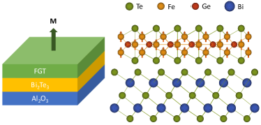
Achieving these properties simultaneously has been challenging. Our initial efforts to integrate room temperature 2D magnet MnSe2 [14] with TI Bi2Se3 produced interdiffusion of Mn into the Bi2Se3 [15] ultimately leading to the formation of MnBi2Se4, a magnetic topological insulator with layered antiferromagnetic order at low temperatures ( 10 K) [16]. Alternatively, a promising material is Fe3GeTe2 (atomic structure shown in Fig. 1a), which has a relatively high of K for bulk crystals and a strong perpendicular magnetic anisotropy (PMA). In addition to Fe3GeTe2, there have been a few reports of ferromagnets with higher among the FemGenTe2 (FGT) family. Bulk Fe5Ge2Te2 was synthesized and characterized to have large PMA up to K [17], while bulk Fe5GeTe2 has a of K [18]. Bulk Fe4GeTe2 was reported to show a of K [19]. Recently, 4 nm Fe4GeTe2 films grown on sapphire by MBE were reported to show a of K, with tunable magnetic anisotropy by slightly varying the Fe concentration [20]. Also, epitaxial growth of Fe5GeTe2 with weak PMA and a of K was achieved by MBE [21]. Furthermore, above room temperature has been observed for Fe3GeTe2 in a variety of contexts including electrostatic gating using ionic liquids [22], patterning-induced enhancement of [23], and through ion intercalation in which case a large variation in the density of states (DOS) at the Fermi level due to extreme electron doping induced by the ionic gate leads to modulation in the ferromagnetism [24]. Deposition of Fe3GeTe2 onto Bi2Te3 has also been reported to help elevate of Fe3GeTe2 [8]. However, the origins of the enhanced remain unclear.
To address the important issue of enhancement, it is essential to systematically investigate the relationship between the magnetic properties and atomic-scale structure of FGT and FGT/TI heterostructures. To this end, molecular beam epitaxy (MBE) and scanning transmission electron microscopy (STEM) are ideal complementary tools that respectively provide atomically-precise layer-by-layer deposition and cross-sectional imaging with atomic resolution. Furthermore, several groups have successfully applied MBE to synthesize Fe3GeTe2 films [25, 26, 8, 27].
In this Letter, we utilize MBE and STEM to demonstrate the systematic tuning of in Fe3GeTe2/Bi2Te3 from bulk-like values (220 K) to above room temperature by varying the growth conditions. Specifically, we investigate the growth of Fe3GeTe2 films onto Bi2Te3 with growth temperatures from 300 C to 375 C. Using reflection high-energy electron diffraction (RHEED) during growth, we observe streaky patterns that indicate high-quality epitaxial growth with well-defined in-plane orientation for all growth temperatures. Through variable-temperature magneto-optic measurements, we find that samples grown at 300 C exhibit a of K, similar to bulk Fe3GeTe2. Increasing the growth temperature systematically enhances , and the exceeds 320 K for samples grown at 375 C. Origins of the enhancement are identified through surprising observations by cross-sectional STEM. While growth at 325 C produces uniform Fe3GeTe2 on Bi2Te3, STEM images of samples grown at 375 C reveal the spontaneous formation of different FemGenTe2 compositions including those with thicker vdW layers (e.g. Fe5Ge2Te2 and Fe7Ge6Te2) and evidence of intercalation in the van der Waals gap. This signifies the onset of a new growth window that supports the formation of multiple members of the FGT family, and importantly, the interface with Bi2Te3 remains very sharp. These observations constitute a major advance enabling the future integration of a broader family of FGT materials (FemGenTe2) with topological insulators, while keeping the high quality of both the 2D magnet and TI layers.
II Epitaxial growth and structural characterization
 \SetHorizontalCoffin\labelcoffin
(a)\SetVerticalPole\imagecoffinleft-2pt+\CoffinWidth\labelcoffin/2\SetVerticalPole\imagecoffinright\Width-3pt-\CoffinWidth\labelcoffin/2\SetHorizontalPole\imagecoffinup\Height+5pt-\CoffinHeight\labelcoffin/2\SetHorizontalPole\imagecoffindown3pt+\CoffinHeight\labelcoffin/2\JoinCoffins\imagecoffin[left,up]\labelcoffin[vc,hc]\TypesetCoffin\imagecoffin
 \SetHorizontalCoffin\labelcoffin
(b)\SetVerticalPole\imagecoffinleft-2pt+\CoffinWidth\labelcoffin/2\SetVerticalPole\imagecoffinright\Width-3pt-\CoffinWidth\labelcoffin/2\SetHorizontalPole\imagecoffinup\Height+5pt-\CoffinHeight\labelcoffin/2\SetHorizontalPole\imagecoffindown3pt+\CoffinHeight\labelcoffin/2\JoinCoffins\imagecoffin[right,down]\labelcoffin[vc,hc]\TypesetCoffin\imagecoffin
 \SetHorizontalCoffin\labelcoffin
(c)\SetVerticalPole\imagecoffinleft-2pt+\CoffinWidth\labelcoffin/2\SetVerticalPole\imagecoffinright\Width-3pt-\CoffinWidth\labelcoffin/2\SetHorizontalPole\imagecoffinup\Height+5pt-\CoffinHeight\labelcoffin/2\SetHorizontalPole\imagecoffindown3pt+\CoffinHeight\labelcoffin/2\JoinCoffins\imagecoffin[right,down]\labelcoffin[vc,hc]\TypesetCoffin\imagecoffin
 \SetHorizontalCoffin\labelcoffin
(d)\SetVerticalPole\imagecoffinleft-2pt+\CoffinWidth\labelcoffin/2\SetVerticalPole\imagecoffinright\Width-3pt-\CoffinWidth\labelcoffin/2\SetHorizontalPole\imagecoffinup\Height+5pt-\CoffinHeight\labelcoffin/2\SetHorizontalPole\imagecoffindown3pt+\CoffinHeight\labelcoffin/2\JoinCoffins\imagecoffin[right,down]\labelcoffin[vc,hc]\TypesetCoffin\imagecoffin
 \SetHorizontalCoffin\labelcoffin
(e)\SetVerticalPole\imagecoffinleft-2pt+\CoffinWidth\labelcoffin/2\SetVerticalPole\imagecoffinright\Width-3pt-\CoffinWidth\labelcoffin/2\SetHorizontalPole\imagecoffinup\Height+5pt-\CoffinHeight\labelcoffin/2\SetHorizontalPole\imagecoffindown3pt+\CoffinHeight\labelcoffin/2\JoinCoffins\imagecoffin[right,down]\labelcoffin[vc,hc]\TypesetCoffin\imagecoffin
For all FGT films grown, we targeted the Fe3GeTe2 composition but found that the resulting material could be more complex. The FGT/Bi2Te3 films are deposited in a Veeco 930 MBE system with a base pressure of Torr. The Al2O3(0001) substrates (MTI Corporation) are prepared by sonication in acetone, methanol and isopropyl alcohol for 5 min each before being annealed in air for 3 hours at 1000 °C. Then substrates are mounted on Omicron flag style paddles, held in a Veeco UNI-Block with paddle adapter, and loaded into the MBE chamber. After degassing at 800 °C for an hour, the Al2O3 substrates are cooled down to 255 °C for starting the growth of FGT/Bi2Te3 heterostructure films. For synthesis, we first grow the Bi2Te3 layer on Al2O3(0001) substrate by co-depositing Bi (99.95%, Alfa Aesar) and Te (99.9999%, United Mineral Corp.) with an atomic flux ratio of 1:15. The high-quality Bi2Te3 films are synthesized by a two-step growth method [28] with a lower temperature (255 °C) in the first step and a relatively higher temperature (295 °C) in the second step both with a growth rate of 0.03 Å /s. Then the FGT films on top of Bi2Te3 are grown by co-depositing Fe (99.99%, Alfa Aesar), Ge (99.9999%, Alfa Aesar), and Te with an atomic flux ratio of 3:1:20, as measured by a beam flux monitor (BFM) and calibrated by x-ray reflectivity (XRR) of elemental films. The growth rate for FGT films is 0.09 Å /s. We note that during all temperature ramping procedures, the film was always exposed to an overpressure of Te flux. At the end of the growth, samples are moved from the growth chamber to the buffer chamber to be cooled down relatively quickly from growth temperature to prevent possible structural change or Te deficiency of the film surface. The growth temperatures are read by a thermocouple behind the paddle and UNI-Block and in the center of the heater, so the actual temperature of the substrate could be lower than the thermocouple reading. After growth, all the samples in this study are transferred via an ultrahigh-vacuum suitcase to another chamber where they are capped with 10 nm of CaF2 to protect against oxidation.
We investigate the structural properties of the FGT/Bi2Te3 heterostructures using a wide range of characterization techniques. In situ reflection high energy electron diffraction (RHEED) is employed to investigate the crystal structure and flatness of the surface during growth. After growth, we utilize x-ray diffraction (XRD) to probe the bulk crystal structure (see Supplementary Material [29], Section 1) and cross-sectional scanning transmission electron microscopy (STEM) to probe the atomic scale structure. The chemical composition is determined by electron energy loss spectroscopy (EELS) as follows. The material structure is first obtained by high-angle annular dark-field (HAADF) and bright field (BF) imaging, and EELS is then performed at each position so that the line cut of EELS is registered to the atomic structure. The EELS line cut along the growth direction () is obtained by integrating over the horizontal plane at specific -positions within the specimen.
 \SetHorizontalCoffin\labelcoffin
(a)\SetVerticalPole\imagecoffinleft-2pt+\CoffinWidth\labelcoffin/2\SetVerticalPole\imagecoffinright\Width-3pt-\CoffinWidth\labelcoffin/2\SetHorizontalPole\imagecoffinup\Height+5pt-\CoffinHeight\labelcoffin/2\SetHorizontalPole\imagecoffindown3pt+\CoffinHeight\labelcoffin/2\JoinCoffins\imagecoffin[left,up]\labelcoffin[vc,hc]\TypesetCoffin\imagecoffin
 \SetHorizontalCoffin\labelcoffin
(b)\SetVerticalPole\imagecoffinleft-2pt+\CoffinWidth\labelcoffin/2\SetVerticalPole\imagecoffinright\Width-3pt-\CoffinWidth\labelcoffin/2\SetHorizontalPole\imagecoffinup\Height+5pt-\CoffinHeight\labelcoffin/2\SetHorizontalPole\imagecoffindown3pt+\CoffinHeight\labelcoffin/2\JoinCoffins\imagecoffin[left,up]\labelcoffin[vc,hc]\TypesetCoffin\imagecoffin
 \SetHorizontalCoffin\labelcoffin
(c)\SetVerticalPole\imagecoffinleft-2pt+\CoffinWidth\labelcoffin/2\SetVerticalPole\imagecoffinright\Width-3pt-\CoffinWidth\labelcoffin/2\SetHorizontalPole\imagecoffinup\Height+5pt-\CoffinHeight\labelcoffin/2\SetHorizontalPole\imagecoffindown3pt+\CoffinHeight\labelcoffin/2\JoinCoffins\imagecoffin[left,up]\labelcoffin[vc,hc]\TypesetCoffin\imagecoffin
 \SetHorizontalCoffin\labelcoffin
(d)\SetVerticalPole\imagecoffinleft-2pt+\CoffinWidth\labelcoffin/2\SetVerticalPole\imagecoffinright\Width-3pt-\CoffinWidth\labelcoffin/2\SetHorizontalPole\imagecoffinup\Height+5pt-\CoffinHeight\labelcoffin/2\SetHorizontalPole\imagecoffindown3pt+\CoffinHeight\labelcoffin/2\JoinCoffins\imagecoffin[left,up]\labelcoffin[vc,hc]\TypesetCoffin\imagecoffin
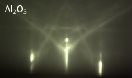
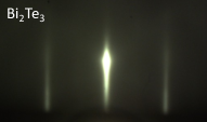
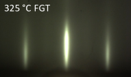
We characterize the epitaxial growth using RHEED, which exhibits streaky patterns throughout the entire growth of the FGT/Bi2Te3/Al2O3(0001) heterostructure. Beginning with the Al2O3 substrate (Figure 1b), the growth of 8 nm Bi2Te3 produces streaky patterns indicative of two-dimensional epitaxial growth (Figure 1c). Following the deposition of 4 nm of FGT ( vdW layers) onto the Bi2Te3 layer, we observe streaky patterns as shown in Figures 1d and 1e for FGT growth temperatures of 325 C and 375 C, respectively. These patterns are characteristic of high-quality two-dimensional layer-by-layer growth with atomically-flat terraces of finite size. The in-plane lattice constant of our FGT films extracted from RHEED patterns is Å, which is very close to the reported values Å for FGT in the literature [30, 31, 26]. In terms of crystallographic properties, the uniformly spaced streaks indicate that the FGT lattice remains aligned with the Bi2Te3 underlayer. In addition, the streaky patterns are maintained throughout the growth, which suggests a high crystalline quality of the interface. RHEED patterns for 300 C and 350 C growths are shown in the Supplementary Material [29] Section 2.
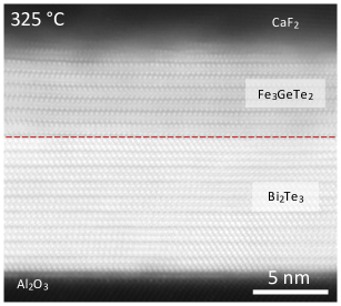
To investigate the crystal structure of the samples, we utilize HAADF-STEM for atomic-scale imaging of the cross-section. Figure 2a shows an image for a 6.4 nm ( vdW layers) FGT film grown at 325C on Bi2Te3, acquired along the FGT [110] direction. vdW gaps are distinguished clearly for both the FGT and Bi2Te3, indicating high-quality vdW layers. In addition, the interface between FGT and Bi2Te3 indicated by the dashed red line is very sharp and free of any secondary phases.
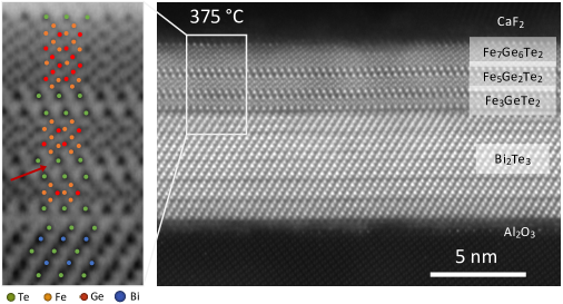
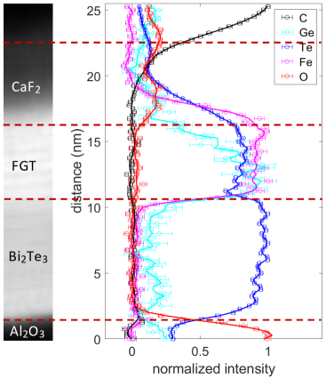
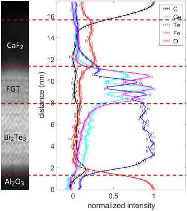
The right image of Fig. 2b shows a HAADF image for an FGT/Bi2Te3 film intended to have 4 nm of Fe3GeTe2 using a growth temperature of 375C. vdW layers are again easily distinguished throughout the entire film, however, the FGT vdW layers appear to be not only Fe3GeTe2 layers but also compositions of thicker FGT layers, as opposed to the uniform thicknesses in the 325°C sample. We identify at least three different compositions of FGT layers in the HAADF images. The left image of Fig. 2b is a magnified bright field (BF) image with the Fe, Ge, Bi, and Te atoms marked out by dots of different colors. Because the brightness of atoms in the BF (HAADF) image is sensitive to atomic number and heavier atoms appear to be darker (brighter), we can distinguish Fe, Ge, and Te from the contrast and make a reasonable estimation about the FGT composition. Based on such analysis of the BF and HAADF images, besides Fe3GeTe2, we can see the existence of thicker cousins like Fe5Ge2Te2 and Fe7Ge6Te2 are also stabilized simultaneously in our film at the temperature of 375°C. We also notice that there are intercalants in the vdW gaps (one is indicated by the red arrow), and we estimate they are Fe atoms based on the lower concentration of Fe in the thicker FGT layers. The dependence of the Fe and Ge concentrations with depth (along the growth direction) is shown in the normalized EELS line profiles (Fig. 2d), which illustrates the variation of the chemical composition within the FGT layers.
The atomic structures of Bi2Te3, Fe3GeTe2 and Fe5Ge2Te2 observed in our sample match very well with what has been reported in the literature. The out-of-plane lattice constants for Bi2Te3, Fe3GeTe2, and Fe5Ge2Te2 are 30.450 Å [32], 16.333 Å [30] and 10.778 Å [17] where the unit cell contains 3, 2, and 1 vdW layers respectively, leading to the thickness of the vdW layers to be 10.150 Å, 8.167 Å and 10.778 Å. In our samples, the Bi2Te3 and Fe3GeTe2 vdW layers have thicknesses of 10.492 Å and 8.290 Å, which agree with the literature values of 10.150 Å and 8.167 Å, respectively [32, 30]. The vdW monolayer of Fe5Ge2Te2 indicates a thickness of 11.183 Å, which is close to the literature value 10.778 Å [17]. On the other hand, the top Fe7Ge6Te2 vdW layer exhibits a thickness of 16.685 Å, and to our knowledge, such films have not been observed previously in experiments.
III Magnetic properties
The magneto-optical technique of reflective magnetic circular dichroism (MCD) enables us to measure out-of-plane magnetic hysteresis loops of the FGT/Bi2Te3 heterostructures. A continuous wave 532 nm laser is focused onto the sample with a angle of incidence and the reflected beam intensity () is measured using a photodiode detector (Thorlabs PDA36A2). The polarization of the incident beam is modulated between right-circular polarized (RCP) and left-circular polarized (LCP) at a frequency of 50 kHz using a photoelastic modulator (PEM) (Hinds Instruments) and the MCD ratio is measured using a lock-in amplifier (Signal Recovery 7270). We apply a magnetic field along the surface normal to measure out-of-plane magnetic hysteresis loops and hold the sample under vacuum in an optical cryostat to vary the temperature. The typical magnetic field ramp rate for the hysteresis loop is 1000 Oe/s and the presented loop is an average over several (typically 5-20) scans. The fast field ramp rate is enabled by using a data acquisition card (National Instruments PCIe-6323) to control the electromagnet current supply (Kepco BOP) via analog output voltage and to read the lock-in amplifier via analog input voltage. A typical acquisition rate is 20 ms per data point with a lock-in time constant of 5 ms, which provides lock-in averaging over 250 cycles (50 kHz 5 ms). The fast acquisition helps avoid drift of the MCD signal.
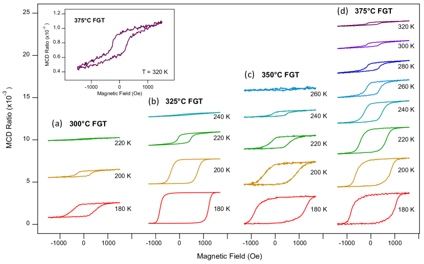
Figure 3 shows representative hysteresis loops measured on 4 nm FGT samples grown on Bi2Te3 at C (a), C (b), C (c), and C (d). All four samples have some common characteristics. They exhibit perpendicular magnetic anisotropy with square hysteresis loops of nearly 100% remanence at low temperatures. The coercivity increases as the measurement temperature is lowered, and we are unable to capture full hysteresis loops at temperatures below those shown in Figure 3 due to the limited range of magnetic field of the measurement system ( Oe).
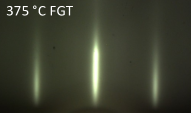
One of the most interesting aspects of the data is the variation of with growth temperature. In all samples, the magnitude of the MCD decreases as the measurement temperature is increased. The trend of enhancement with increasing growth temperature is visible from the hysteresis loops. For the 300 C sample, the remanence appears to be smaller and disappears at K, which is consistent with the bulk of FGT. However, at the same 220 K temperature, the 325 C grown sample shows a very clear opening in the hysteresis loop, which persists up to K. In the meantime, we notice that the shape of the hysteresis loops for the 325 C sample is more square compared to the others. Similarly, continues to increase with higher growth temperatures 350 C and 375 C. Interestingly, the remanence is still observed to be present at 320 K for the C sample, which is zoomed in and shown in the inset of Figure 3.
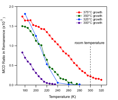
In Figure 4, we provide a better illustration of the temperature dependence of the magnetization by plotting the magnetic remanence as a function of temperature for all the hysteresis loops in the temperature scan. Here, the MCD ratio in remanence is defined as . In this plot, the systematic variation of with the growth temperature is clear. For the 300 C sample, the is K which is consistent with the bulk of FGT. Increasing the growth temperature to 325 C and 350 C leads to increased of K and K, respectively. Finally, for the 375 C sample, the ferromagnetism persists beyond room temperature to above 320 K, the maximum temperature of our measurement system.
IV Discussion
Based on the HAADF STEM images of the 325°C and 375°C FGT/Bi2Te3 samples, we learn that the higher temperature growths of FGT on Bi2Te3 lead to the formation of thicker vdW FGT layers with varying stoichiometry of Fe. Specifically, there is coexistence of Fe3GeTe2, Fe5Ge2Te2 and Fe7Ge6Te2 in our 375°C grown FGT. The most well-known composition of FemGemTe2 is Fe3GeTe2, which has been reported to have a bulk TC of 220-230 K. This value is consistent with our 300°C and 325°C samples with mostly uniform vdW Fe3GeTe2 layers showing up in the STEM images. For the Fe5Ge2Te2 layer, however, it is reported to have a TC of 250 K and possess a large PMA [17]. A similar structure Fe5GeTe2 was also reported in literature, and it was synthesized to establish magnetic order up to 310 K for bulk materials and 280 K for thin exfoliated flakes [18]. As for the thickest vdW FGT layer Fe7Ge6Te2 that we observed in the 375°C sample, the magnetic properties of it are still unknown. It is possible that with the increased number of Fe atoms in one vdW layer, TC of this component could be even higher. In the literature, monolayer Fe7GeTe2 was calculated to have a TC of 570 K [33]. But there has been no report of measurements on Fe7Ge6Te2 so far. Intercalants are also observed in the vdW gaps. Recent studies show that Fe intercalants in the vdW gaps of Fe3GeTe2 are responsible for the enhancement of from 160 K to 230 K in bulk crystals [34]. Thus, the elevated Curie temperature may be due to a combination of different thicker layers of FemGenTe2 in the film, the interlayer coupling/proximity effect between them, and intercalants in the vdW layers.
Looking back at our temperature-dependent growths, it is rather surprising that the temperature 375°C could help stabilize three different layers of FGT at the same time, with each of them containing a different stoichiometry of Fe respectively. At relatively lower temperatures, the stoichiometry of Fe3GeTe2 seems to be the most energetically favored state. From what we have seen in the STEM images, when we use a higher growth temperature, the Fe and Ge atoms are more likely to bond together to form thicker Fe-Ge layers before the Te atoms come into play and separate them. Thus, at higher growth temperatures, the greater mobility of the atoms enables epitaxial stabilization of different material phases of the FGT family.
Our findings reveal the possibility of integrating different compositions of FGT on topological insulators, with still a very sharp interface in between. At this particular temperature (of 375°C), all the parameters delicately balance with each other and lead to coexistence of different phases of FGT. This offers a playground for interesting growths of 2D magnet FGT/TI heterostructures with a lot of tunability. If we consider breaking the balance by tuning growth conditions, it might become possible to stabilize targeted FemGenTe2 compositions for tailored magnetic properties of the heterostructures. As we have studied in our previous work of kinetically controlled FGT growth on Ge substrates [27], the growth rate can also be a useful knob to tune, stabilize and optimize certain components of our vdW material during growth. There are also many other important parameters such as the Fe:Ge atomic ratio that could be changed accurately to help tune composition of our material. Fine tuning of the temperature could also play an important role. With these knobs, we can anticipate that tailoring the properties of the 2D magnet/TI heterostructures will become easier and more versatile.
V Conclusion
In summary, we demonstrate tuning of the Curie temperature to above room temperature in MBE-grown FGT/Bi2Te3 heterostructures by varying growth conditions. Specifically, variable-temperature magneto-optic measurements reveal that higher growth temperatures lead to higher Curie temperatures, with sample growth at 375°C exhibiting ferromagnetism that persists to over 320 K. Cross-sectional STEM imaging of samples grown at 325C and 375C identifies differences in the atomic-scale structure. Compared to FGT films grown at lower temperatures (325°C), in which we have uniform Fe3GeTe2 layers integrated with Bi2Te3, thicker vdW layers in the FGT family and intercalation (likely Fe atoms) are also observed for growth at 375°C. We find that highly-ordered Fe5Ge2Te2 and Fe7Ge6Te2 coexist with Fe3GeTe2, while still keeping the interface with Bi2Te3 sharp and clean. The thicker FGT layers and intercalation that form in the higher-temperature growths both likely contribute to the enhanced Curie temperature because a number of members in FGT family with more Fe atoms in the single vdW layer have been reported and/or predicted to have higher Curie temperatures than Fe3GeTe2 (TC 220 K), and Fe intercalants could enhance the interlayer coupling. These are very interesting systems for spintronics devices and for studying phenomena related to the topological surface states, especially since ferromagnetism is realized above room temperature, high-quality interfaces are preserved, and epitaxial growth enables scalability.
Acknowledgements
The research at Ohio State was supported by the AFOSR/MURI project 2DMagic (FA9550-19-1-0390) and the US Department of Energy (DE-SC0016379). K.R. was supported by DAGSI (RX22-OSU-22-1). I.L. was supported by the Center for Emergent Materials, an NSF MRSEC (DMR-2011876). The research at Cornell was supported by the AFOSR/MURI project 2DMagic (FA9550-19-1-0390) and the US National Science Foundation (DMR-2104268). T.M.J.C. was supported by the Singapore Agency for Science, Technology, and Research, and Y.K.L. acknowledges the Cornell Presidential Postdoctoral Fellowship. The work utilized the shared facilities of the Cornell Center for Materials Research (supported by the NSF via grant DMR-1719875) and the Cornell NanoScale Facility, a member of the National Nanotechnology Coordinated Infrastructure (supported by the NSF via grant NNCI-2025233).
References
- Liu et al. [2016] Y. Liu, N. O. Weiss, X. Duan, H.-C. Cheng, Y. Huang, and X. Duan, Van der Waals heterostructures and devices, Nature Reviews Materials 1, 1 (2016).
- Novoselov et al. [2016] K. S. Novoselov, A. Mishchenko, A. Carvalho, and A. H. Castro Neto, 2D materials and van der Waals heterostructures, Science 353, aac9439 (2016).
- Wang et al. [2022] Q. H. Wang, A. Bedoya-Pinto, M. Blei, A. H. Dismukes, A. Hamo, S. Jenkins, M. Koperski, Y. Liu, Q.-C. Sun, E. J. Telford, H. H. Kim, M. Augustin, U. Vool, J.-X. Yin, L. H. Li, A. Falin, C. R. Dean, F. Casanova, R. F. L. Evans, M. Chshiev, A. Mishchenko, C. Petrovic, R. He, L. Zhao, A. W. Tsen, B. D. Gerardot, M. Brotons-Gisbert, Z. Guguchia, X. Roy, S. Tongay, Z. Wang, M. Z. Hasan, J. Wrachtrup, A. Yacoby, A. Fert, S. Parkin, K. S. Novoselov, P. Dai, L. Balicas, and E. J. G. Santos, The Magnetic Genome of Two-Dimensional van der Waals Materials, ACS Nano 16, 6960 (2022).
- Gibertini et al. [2019] M. Gibertini, M. Koperski, A. F. Morpurgo, and K. S. Novoselov, Magnetic 2D materials and heterostructures, Nature Nanotechnology 14, 408 (2019).
- Li et al. [2022] Y. Li, B. Yang, S. Xu, B. Huang, and W. Duan, Emergent Phenomena in Magnetic Two-Dimensional Materials and van der Waals Heterostructures, ACS Applied Electronic Materials 4, 3278 (2022).
- Hou et al. [2019] Y. Hou, J. Kim, and R. Wu, Magnetizing topological surface states of Bi2Se3 with a CrI3 monolayer, Science Advances 5, eaaw1874 (2019).
- Mogi et al. [2019] M. Mogi, T. Nakajima, V. Ukleev, A. Tsukazaki, R. Yoshimi, M. Kawamura, K. S. Takahashi, T. Hanashima, K. Kakurai, T.-h. Arima, M. Kawasaki, and Y. Tokura, Large Anomalous Hall Effect in Topological Insulators with Proximitized Ferromagnetic Insulators, Physical Review Letters 123, 016804 (2019).
- Wang et al. [2020] H. Wang, Y. Liu, P. Wu, W. Hou, Y. Jiang, X. Li, C. Pandey, D. Chen, Q. Yang, H. Wang, D. Wei, N. Lei, W. Kang, L. Wen, T. Nie, W. Zhao, and K. L. Wang, Above Room-Temperature Ferromagnetism in Wafer-Scale Two-Dimensional van der Waals Fe3GeTe2 Tailored by a Topological Insulator, ACS Nano 14, 10045 (2020).
- Mogi et al. [2021] M. Mogi, K. Yasuda, R. Fujimura, R. Yoshimi, N. Ogawa, A. Tsukazaki, M. Kawamura, K. S. Takahashi, M. Kawasaki, and Y. Tokura, Current-induced switching of proximity-induced ferromagnetic surface states in a topological insulator, Nature Communications 12, 1404 (2021).
- Liu and Hesjedal [2021] J. Liu and T. Hesjedal, Magnetic Topological Insulator Heterostructures: A Review, Advanced Materials , 2102427 (2021).
- Mellnik et al. [2014] A. R. Mellnik, J. S. Lee, A. Richardella, J. L. Grab, P. J. Mintun, M. H. Fischer, A. Vaezi, A. Manchon, E.-A. Kim, N. Samarth, and D. C. Ralph, Spin-transfer torque generated by a topological insulator, Nature 511, 449 (2014).
- Chang et al. [2013] C.-Z. Chang, J. Zhang, X. Feng, J. Shen, Z. Zhang, M. Guo, K. Li, Y. Ou, P. Wei, L.-L. Wang, Z.-Q. Ji, Y. Feng, S. Ji, X. Chen, J. Jia, X. Dai, Z. Fang, S.-C. Zhang, K. He, Y. Wang, L. Lu, X.-C. Ma, and Q.-K. Xue, Experimental Observation of the Quantum Anomalous Hall Effect in a Magnetic Topological Insulator, Science 340, 167 (2013).
- Deng et al. [2020] Y. Deng, Y. Yu, M. Z. Shi, Z. Guo, Z. Xu, J. Wang, X. H. Chen, and Y. Zhang, Quantum anomalous Hall effect in intrinsic magnetic topological insulator MnBi2Te4, Science 367, 895 (2020).
- O’Hara et al. [2018] D. J. O’Hara, T. Zhu, A. H. Trout, A. S. Ahmed, Y. K. Luo, C. H. Lee, M. R. Brenner, S. Rajan, J. A. Gupta, D. W. McComb, and R. K. Kawakami, Room Temperature Intrinsic Ferromagnetism in Epitaxial Manganese Selenide Films in the Monolayer Limit, Nano Letters 18, 3125 (2018).
- Noesges et al. [2020] B. A. Noesges, T. Zhu, J. J. Repicky, S. Yu, F. Yang, J. A. Gupta, R. K. Kawakami, and L. J. Brillson, Chemical migration and dipole formation at van der Waals interfaces between magnetic transition metal chalcogenides and topological insulators, Physical Review Materials 4, 054001 (2020).
- Zhu et al. [2021] T. Zhu, A. J. Bishop, T. Zhou, M. Zhu, D. J. O’Hara, A. A. Baker, S. Cheng, R. C. Walko, J. J. Repicky, T. Liu, J. A. Gupta, C. M. Jozwiak, E. Rotenberg, J. Hwang, I. Žutić, and R. K. Kawakami, Synthesis, Magnetic Properties, and Electronic Structure of Magnetic Topological Insulator MnBi2Se4, Nano Letters 21, 5083 (2021).
- Jothi et al. [2020] P. R. Jothi, J. P. Scheifers, Y. Zhang, M. Alghamdi, D. Stekovic, M. E. Itkis, J. Shi, and B. P. T. Fokwa, Fe5-xGe2Te2—a New Exfoliable Itinerant Ferromagnet with High Curie Temperature and Large Perpendicular Magnetic Anisotropy, Physica Status Solidi (RRL) – Rapid Research Letters 14, 1900666 (2020).
- May et al. [2019] A. F. May, D. Ovchinnikov, Q. Zheng, R. Hermann, S. Calder, B. Huang, Z. Fei, Y. Liu, X. Xu, and M. A. McGuire, Ferromagnetism Near Room Temperature in the Cleavable van der Waals Crystal Fe5GeTe2, ACS Nano 13, 4436 (2019).
- Seo et al. [2020] J. Seo, D. Y. Kim, E. S. An, K. Kim, G.-Y. Kim, S.-Y. Hwang, D. W. Kim, B. G. Jang, H. Kim, G. Eom, S. Y. Seo, R. Stania, M. Muntwiler, J. Lee, K. Watanabe, T. Taniguchi, Y. J. Jo, J. Lee, B. I. Min, M. H. Jo, H. W. Yeom, S.-Y. Choi, J. H. Shim, and J. S. Kim, Nearly room temperature ferromagnetism in a magnetic metal-rich van der Waals metal, Science Advances 6, eaay8912 (2020).
- Wang et al. [2023] H. Wang, H. Lu, Z. Guo, A. Li, P. Wu, J. Li, W. Xie, Z. Sun, P. Li, H. Damas, A. M. Friedel, S. Migot, J. Ghanbaja, L. Moreau, Y. Fagot-Revurat, S. Petit-Watelot, T. Hauet, J. Robertson, S. Mangin, W. Zhao, and T. Nie, Interfacial engineering of ferromagnetism in wafer-scale van der Waals Fe4GeTe2 far above room temperature, Nature Communications 14, 2483 (2023).
- Ribeiro et al. [2022] M. Ribeiro, G. Gentile, A. Marty, D. Dosenovic, H. Okuno, C. Vergnaud, J.-F. Jacquot, D. Jalabert, D. Longo, P. Ohresser, A. Hallal, M. Chshiev, O. Boulle, F. Bonell, and M. Jamet, Large-scale epitaxy of two-dimensional van der Waals room-temperature ferromagnet Fe5GeTe2, npj 2D Materials and Applications 6, 1 (2022).
- Deng et al. [2018] Y. Deng, Y. Yu, Y. Song, J. Zhang, N. Z. Wang, Z. Sun, Y. Yi, Y. Z. Wu, S. Wu, J. Zhu, J. Wang, X. H. Chen, and Y. Zhang, Gate-tunable room-temperature ferromagnetism in two-dimensional Fe3GeTe2, Nature 563, 94 (2018).
- Li et al. [2018] Q. Li, M. Yang, C. Gong, R. V. Chopdekar, A. T. N’Diaye, J. Turner, G. Chen, A. Scholl, P. Shafer, E. Arenholz, A. K. Schmid, S. Wang, K. Liu, N. Gao, A. S. Admasu, S.-W. Cheong, C. Hwang, J. Li, F. Wang, X. Zhang, and Z. Qiu, Patterning-Induced Ferromagnetism of Fe3GeTe2 van der Waals Materials beyond Room Temperature, Nano Letters 18, 5974 (2018).
- Li et al. [2021] Y. Li, H. Yan, B. Xu, L. Zhen, and C.-Y. Xu, Electrochemical Intercalation in Atomically Thin van der Waals Materials for Structural Phase Transition and Device Applications, Advanced Materials 33, 2000581 (2021).
- Liu et al. [2017] S. Liu, X. Yuan, Y. Zou, Y. Sheng, C. Huang, E. Zhang, J. Ling, Y. Liu, W. Wang, C. Zhang, J. Zou, K. Wang, and F. Xiu, Wafer-scale two-dimensional ferromagnetic Fe3GeTe2 thin films grown by molecular beam epitaxy, npj 2D Materials and Applications 1, 1 (2017).
- Roemer et al. [2020] R. Roemer, C. Liu, and K. Zou, Robust ferromagnetism in wafer-scale monolayer and multilayer Fe3GeTe2, npj 2D Materials and Applications 4, 1 (2020).
- Zhou et al. [2022] W. Zhou, A. J. Bishop, M. Zhu, I. Lyalin, R. Walko, J. A. Gupta, J. Hwang, and R. K. Kawakami, Kinetically Controlled Epitaxial Growth of Fe3GeTe2 van der Waals Ferromagnetic Films, ACS Applied Electronic Materials 4, 3190 (2022).
- Harrison et al. [2013] S. E. Harrison, S. Li, Y. Huo, B. Zhou, Y. L. Chen, and J. S. Harris, Two-step growth of high quality Bi2Te3 thin films on Al2O3 (0001) by molecular beam epitaxy, Applied Physics Letters 102, 171906 (2013).
- [29] See Supplementary Material for X-ray diffraction data and additional RHEED patterns.
- Deiseroth et al. [2006] H.-J. Deiseroth, K. Aleksandrov, C. Reiner, L. Kienle, and R. K. Kremer, Fe3GeTe2 and Ni3GeTe2 – Two New Layered Transition-Metal Compounds: Crystal Structures, HRTEM Investigations, and Magnetic and Electrical Properties, European Journal of Inorganic Chemistry 2006, 1561 (2006).
- Yi et al. [2016] J. Yi, H. Zhuang, Q. Zou, Z. Wu, G. Cao, S. Tang, S. A. Calder, P. R. C. Kent, D. Mandrus, and Z. Gai, Competing antiferromagnetism in a quasi-2D itinerant ferromagnet: Fe3GeTe2, 2D Materials 4, 011005 (2016).
- Hosokawa et al. [2019] Y. Hosokawa, K. Tomita, and M. Takashiri, Growth of single-crystalline Bi2Te3 hexagonal nanoplates with and without single nanopores during temperature-controlled solvothermal synthesis, Scientific Reports 9, 10790 (2019).
- Liu et al. [2022] Q. Liu, J. Xing, Z. Jiang, Y. Guo, X. Jiang, Y. Qi, and J. Zhao, Layer-dependent magnetic phase diagram in FenGeTe2 () ultrathin films, Communications Physics 5, 1 (2022).
- Wu et al. [2023] Y. Wu, Y. Hu, C. Wang, X. Zhou, X. Hou, W. Xia, Y. Zhang, J. Wang, Y. Ding, J. He, P. Dong, S. Bao, J. Wen, Y. Guo, K. Watanabe, T. Taniguchi, W. Ji, Z. Wang, and J. Li, Fe‐Intercalation Dominated Ferromagnetism of van der Waals Fe3GeTe2, Advanced Materials , 2302568, doi: 10.1002/adma.202302568 (2023).