SSM
Valley-free silicon fins by shear strain
Abstract
Electron spins confined in silicon quantum dots are promising candidates for large-scale quantum computers. However, the degeneracy of the conduction band of bulk silicon introduces additional levels dangerously close to the window of computational energies, where the quantum information can leak. The energy of the valley states - typically - depends on hardly controllable atomistic disorder and still constitutes a fundamental limit to the scalability of these architectures. In this work, we introduce designs of CMOS-compatible silicon fin field-effect transistors that enhance the energy gap to non-computational states by more than one order of magnitude. Our devices comprise realistic silicon-germanium nanostructures with a large shear strain, where troublesome valley degrees of freedom are completely removed. The energy of non-computational states is therefore not affected by unavoidable atomistic disorder and can further be tuned in-situ by applied electric fields. Our design ideas are directly applicable to a variety of setups and will offer a blueprint towards silicon-based large-scale quantum processors.
Introduction.
Spins in silicon and germanium quantum dots (QDs) are the workhorse of modern semiconductor-based quantum technology [1, 2, 3, 4, 5, 6, 7, 8, 9, 10, 11, 12]. The most advanced platforms to date utilize planar heterostructures comprising planar Si and SiGe alloys, where the quantum information is carried by single electrons confined in the Si layer [10, 11, 12, 9, 13]. In these systems, long spin coherence is enabled by the weak spin-orbit interaction of the conduction band and by isotopically purifying Si [14]. Electron spin resonance was harnessed to selectively control individual qubits [15, 16, 17] whereas tunable exchange interactions mediate fast, high-fidelity two-qubit gates [18, 19, 20, 21, 22, 23, 8]. The versatility of these architectures permitted remote coupling of distant qubits via microwave cavities [24, 25, 26] and spin shuttling [27, 28, 29, 30], as well as entanglement of three spin states [31]. Readout and two-qubit gate fidelities exceeding the error correction threshold [32, 33, 13, 34] and the recent demonstration of six-qubit quantum processors [9] constitute promising steps toward large-scale quantum processors.
However, further progress in electron spin qubits in silicon is currently hindered by the valley degeneracy of the silicon conduction band. In planar Si/SiGe heterostructures tensile in-plane strain partially lifts the six-fold degeneracy of bulk silicon, pushing four valleys to higher energy; the groundstate remains two-fold degenerate [35, 36, 37]. The residual valleys introduce troublesome additional levels in the vicinity of the computational energies where the quantum information is processed. These states open the system to decoherence and relaxation channels and constitute a critical source of leakage [38, 39, 40, 41, 42, 43, 44, 45]. The valley degeneracy can be lifted by strong electric fields, but the induced energy gap is relatively small and dangerously close to the typical qubit energies . Because it strongly depends on atomistic details of the Si/SiGe interface, to control this gap reliably and reproducibly is an open challenge [46, 47, 48, 49, 50, 51, 52]. Moreover, in hot qubits, valley states can be thermally excited, hindering the scalability of quantum processors [53]. Larger valley splittings are reached by periodically altering the concentration of Ge in the well [54, 55]. In MOS structures, splittings are reached by tightly confined electrons at the interfaces between Si and SiO2, but these values largely depend on interface disorder [56, 53, 57, 58].
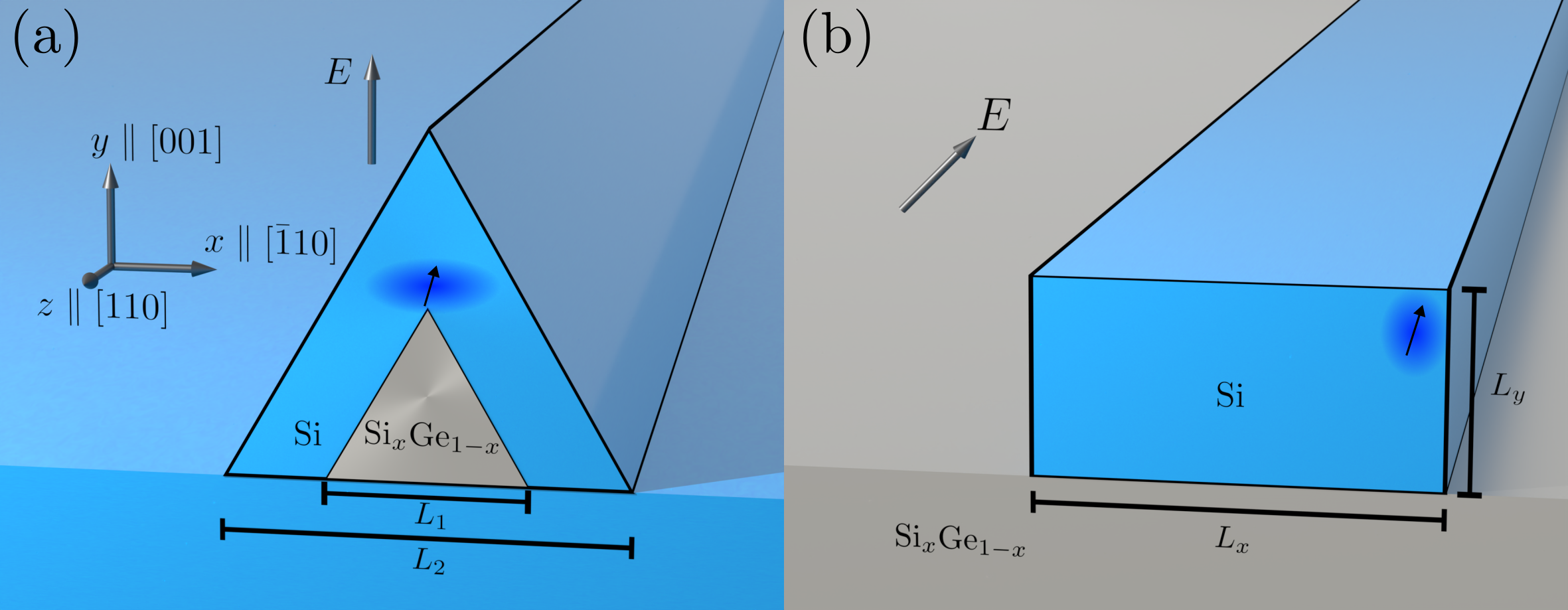
In this work, we propose alternative Si/SiGe nanostructures that completely lift the valley degeneracy and thus provide ideal platforms for future spin-based quantum processors. In our designs the electrons are confined in quasi one-dimensional (1D) Si fins compatible with CMOS technology [59], see Fig. 1, where, in contrast to planar heterostructures, the SiGe induces a large shear strain. By detailed simulations based on continuum elasticity theory and microscopic theory, we show that our engineered strain profile enables a non-degenerate groundstate split from the excited states by energies , two to three orders of magnitude larger than in current devices. Importantly, this energy gap remains large for realistic values of applied electric fields and is independent of atomistic disorder at the interfaces, rendering our design robust in a wide variety of different fins.
Theoretical model.
The conduction band of bulk Si has six degenerate minima in the first Brillouin zone (BZ), which are located at distance from the points. Here is the lattice constant of Si [60]. Its low-energy electronic states are described by the microscopic two-band Hamiltonian [61, 62]:
| (1) |
where is the longitudinal direction, and are the two transversal directions, which are aligned with the main crystallographic axes , , and . The canonical momentum operators are ().
This Hamiltonian is based on a small-momentum expansion of the band structure around the points and the Pauli matrices , with , refer to the two crossing at the point. Because there are three inequivalent points, the six valleys are described by three independent copies of Eq. (1). The spin degree of freedom is not included in . The transversal and longitudinal masses of Si are and , respectively, with being the free electron mass; is the band-coupling mass [61, 63].
The lattice constant of Ge [60] is larger than . Thus, the Si is strained in Si/SiGe heterostructures. The uniaxial strain and the shear strain modify the electron energy depending on the deformation potentials [64, 65] and [61, 66], respectively. In the nanostructures sketched in Fig. 1, we simulate the strain tensor elements by finite-element methods (FEM) based on continuum elasticity theory [67, 68, 69, 70]. More details on the simulation of strain in our setups is provided in the Supplemental Material (SM) [71]. We assume that the lattice constant of an alloy of SixGe1-x changes linearly from to , and thus we use the relation
| (2) |
interpolating linearly from the minimal strain at to the maximal strain at [72, 73].
Eq. (1) includes the homogeneous electric field resulting in the electrostatic potential , with being the electron charge and , and the confinement potential accounting for the cross section of the fin. We model the sharp interface between Si and a SixGe1-x alloy by using the step-like potential function
| (3) |
where indicates the region in the cross section occupied by Si (SixGe1-x ). In analogy to Eq. (2), we also assume that decreases linearly from the maximal value of (the band gap difference between Si and Ge) as - the concentration of Si in the alloy - increases.
Because Si has an anisotropic dispersion relation, we emphasize that electrons lying in the three different pairs of valley states generally experience different confinement potentials. To account for this effect, we fix the direction to be aligned to the fin and the direction to be perpendicular to the substrate, see Fig. 1. We also restrict ourselves to the analysis of Si , with fins that are aligned to the crystallographic axis, i.e. and . This is the standard orientation of current devices [1, 2, 74, 4].
Shear-strain-induced lifting of the valley degeneracy.
The Hamiltonian in Eq. (1) allows us to accurately analyze the physics of the conduction-band electrons in the fins shown in Fig. 1. We discretize in real space for different cross sections with lattice spacings and and we analyze the dispersion relation of the lowest energy states. Importantly, we include the inhomogeneous strain tensor simulated by FEM with COMSOL Multiphysics ® [75], see SM for more details [71].
The effect of strain in our fins is illustrated in Fig. 2(a), where we show the projection of the three-dimensional (3D) bulk valleys in Si onto the 1D BZ along , see Fig. 1. Along , the four bulk Si valleys belonging to the -plane (purple ellipses) are projected close to the points and the two valleys along the axis (turquoise circles) onto the point (). When (dashed gray lines) all valleys are close in energy up to a small contribution caused by the anisotropic confinement. In analogy to planar heterostructures [62, 76, 64, 70] at finite values (blue solid lines) uniaxial strain splits away the states with minimum close to the points by several tens of meV.
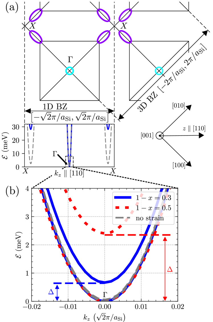
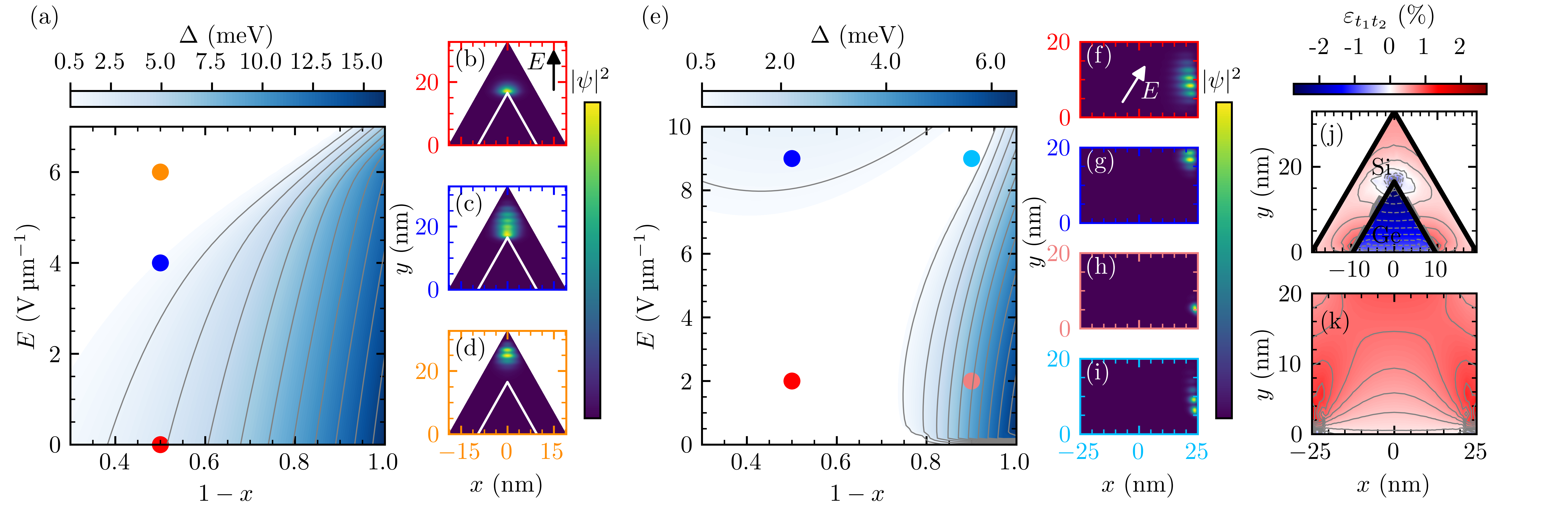
However, the inherent shear strain in our fin devices results in the lifting of the remaining two valleys. A zoom into the dispersion relation in the vicinity of the point, highlighting the shear-strain-induced valley splitting is shown in Fig. 2(b). We focus here on the triangular fin sketched in Fig. 1(a), however, the results discussed are valid also for rectangular fins. Without Ge and the lowest two energy states (dashed gray line) are quasi-degenerate [77, 56], see Eq. (1). The SixGe1-x induces a finite in the Si shell which lifts the valley degeneracy. More details on the simulated strain profile in our fins are provided in Fig. 3 and SM [71]. Considering a moderate Ge concentration of , we estimate the valley splitting for pointing along , significantly larger than what is obtained in planar heterostructures [38, 39, 40, 41, 42, 43, 44, 45]. By increasing the Ge amount to the shear strain increases [see Eq. (2)] and consequently a larger value of is reached. The split states from the same subband at are strongly hybridized.
Because the electron is localized at the top of the Si fin, the substrate does not affect the values of . We emphasize that in striking contrast to valley splittings arising in planar heterostructures, our arises from shear strain and therefore is reproducible and robust against atomistic disorder at the Si/SiGe interfaces [36, 78]. We confirm this robustness with additional simulations shown in the SM [71].
Electric-field-dependence of valley splitting.
In planar Si/SiGe structures, the valley splitting strongly depends on the applied electric field . We show that in our fins, can also be tuned in-situ by , however at large enough concentrations of Ge in the SixGe1-x alloy, remains large and in the meV range.
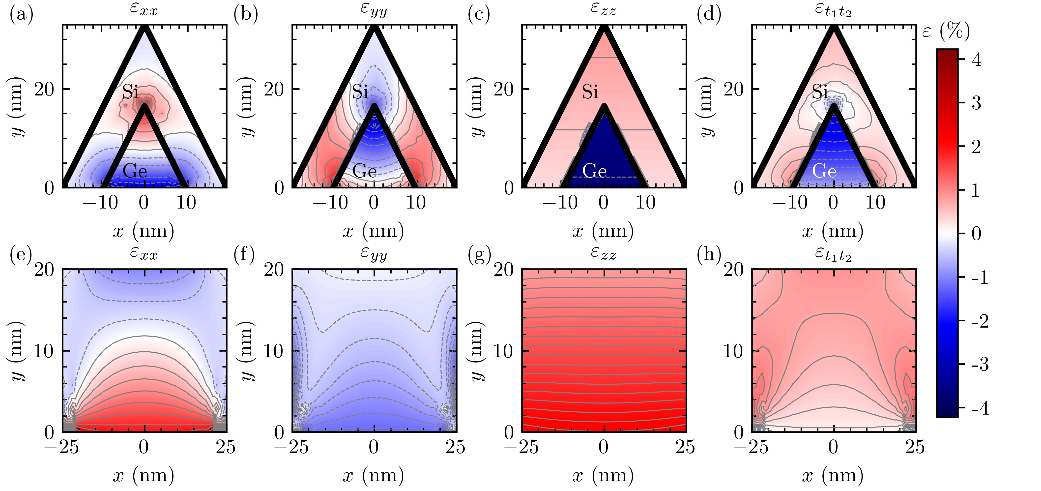
The dependence of on and is analyzed in Fig. 3(a,e). In the triangular fin sketched in Fig. 1(a), a positive electric field to confine an electron tends to decrease . This trend can be understood by observing that shifts the electron wavefunction towards the upper tip of the Si shell [see Fig. 3(b-d)], where shear strain first decreases and then slightly increases with opposite sign, see Fig. 3(j). A detailed explanation of the FEM simulation is provided in the SM [71]. As the concentration of Ge increases, strain also increases, resulting in for a wide range of . Because depends on shear strain, our results are robust against variations in the shape of the cross section. This robustness is verified in the SM [71], where we simulate a rounded fin in a half-circular cross section, and we find similar values of .
Large values of also emerge for a wide range of parameters in the rectangular Si fins on a SiGe substrate sketched in Fig. 1(b). Similar Si nanostructures of comparable size are current state-of-the-art for spin qubits [74, 4, 79, 80] and can be adapted to our proposal by replacing the oxide substrate by SiGe. In this device, we observe in Fig. 3(e-i) a non-trivial interplay of and , which we relate to the position and spacial spread of the wavefunction in the cross section. In this case, we study the effect of an electric field pushing the electron wavefunction towards the upper-right corner of the fin; due to symmetry, the results are equivalent if the electric field pushes the electron towards the upper-left corner. In particular, is maximal at the left and right bottom sides of the fin, see Fig. 3(k), and, thus, is large when the electron is localized close to these areas. We should emphasize, however, that when it is too close to the interface the electron risks to leak into the substrate. In addition, the QD is also easier to control electrostatically when it is localized at an upper corner.
For low concentrations of Ge () electrons are localized at the upper corner of the cross section by a strong field , and thus increases with increasing . For weak the wavefunction is spread over the right side and is small. At larger values of , the inhomogeneous uniaxial strain localizes the electrons close to the edges already at weak , thus resulting in large values of . In this case, is only weakly dependent on , and it decreases with increasing because the electrons are pushed away from the substrate where strain is maximal.
The large valley splitting due to shear strain has important consequences for spin qubits realized in gate-defined QDs in Si fins. The spin qubit lifetime in planar Si/SiGe heterostructures is strongly limited at spin-valley relaxation hot spots where the qubit Zeeman and valley splittings become comparable [49, 50, 41, 56, 81]. These hot spots are naturally avoided in our devices because of the large difference between the typically small qubit Zeeman splitting of and the valley splitting of we predict.
Conclusion.
In this work we show that shear strain substantially enhances the valley splitting in Si/SiGe heterostructures. In realistic Si fins we predict valley splittings , orders of magnitude larger than in current devices. We show that the amplitude of the gap can be engineered by varying the composition of the SixGe1-x alloy and is controllable in-situ by electric fields. Importantly, due to the large valley splitting spin-valley relaxation hot spots are avoided naturally in our proposed Si fins. Our designs are also robust against variations of the fin shape and, in contrast to planar systems, are not affected by atomistic disorder. By removing a critical issue of current electron spin qubits in Si, our devices will push these architectures towards new coherence standards and pave the way towards large-scale semiconductor-based quantum processors.
Acknowledgements.
We thank Dominik Zumbühl for giving access to the license for COMSOL Multiphysics ® and Andreas V. Kuhlmann for useful comments. This work is supported by the Swiss National Science Foundation (SNSF) and NCCR SPIN (Grant No. 51NF40-180604).References
- Geyer et al. [2022] S. Geyer, B. Hetényi, S. Bosco, L. C. Camenzind, R. S. Eggli, A. Fuhrer, D. Loss, R. J. Warburton, D. M. Zumbühl, and A. V. Kuhlmann, (2022), arXiv:2212.02308 [cond-mat.mes-hall] .
- Camenzind et al. [2022] L. C. Camenzind, S. Geyer, A. Fuhrer, R. J. Warburton, D. M. Zumbühl, and A. V. Kuhlmann, Nat. Electron. 5, 178 (2022).
- Hendrickx et al. [2021] N. W. Hendrickx, W. I. L. Lawrie, M. Russ, F. van Riggelen, S. L. de Snoo, R. N. Schouten, A. Sammak, G. Scappucci, and M. Veldhorst, Nature 591, 580 (2021).
- Piot et al. [2022] N. Piot, B. Brun, V. Schmitt, S. Zihlmann, V. P. Michal, A. Apra, J. C. Abadillo-Uriel, X. Jehl, B. Bertrand, H. Niebojewski, L. Hutin, M. Vinet, M. Urdampilleta, T. Meunier, Y.-M. Niquet, R. Maurand, and S. D. Franceschi, Nat. Nanotechnol. 17, 1072 (2022).
- Jirovec et al. [2021] D. Jirovec, A. Hofmann, A. Ballabio, P. M. Mutter, G. Tavani, M. Botifoll, A. Crippa, J. Kukucka, O. Sagi, F. Martins, J. Saez-Mollejo, I. Prieto, M. Borovkov, J. Arbiol, D. Chrastina, G. Isella, and G. Katsaros, Nat. Mater. 20, 1106 (2021).
- Jirovec et al. [2022] D. Jirovec, P. M. Mutter, A. Hofmann, A. Crippa, M. Rychetsky, D. L. Craig, J. Kukucka, F. Martins, A. Ballabio, N. Ares, D. Chrastina, G. Isella, G. Burkard, and G. Katsaros, Phys. Rev. Lett. 128, 126803 (2022).
- Mądzik et al. [2022] M. T. Mądzik, S. Asaad, A. Youssry, B. Joecker, K. M. Rudinger, E. Nielsen, K. C. Young, T. J. Proctor, A. D. Baczewski, A. Laucht, V. Schmitt, F. E. Hudson, K. M. Itoh, A. M. Jakob, B. C. Johnson, D. N. Jamieson, A. S. Dzurak, C. Ferrie, R. Blume-Kohout, and A. Morello, Nature 601, 348 (2022).
- Petit et al. [2022] L. Petit, M. Russ, G. H. G. J. Eenink, W. I. L. Lawrie, J. S. Clarke, L. M. K. Vandersypen, and M. Veldhorst, Commun. Mater. 3, 82 (2022).
- Philips et al. [2022] S. G. J. Philips, M. T. Mądzik, S. V. Amitonov, S. L. de Snoo, M. Russ, N. Kalhor, C. Volk, W. I. L. Lawrie, D. Brousse, L. Tryputen, B. P. Wuetz, A. Sammak, M. Veldhorst, G. Scappucci, and L. M. K. Vandersypen, Nature 609, 919 (2022).
- Unseld et al. [2023] F. K. Unseld, M. Meyer, M. T. Mądzik, F. Borsoi, S. L. de Snoo, S. V. Amitonov, A. Sammak, G. Scappucci, M. Veldhorst, and L. M. K. Vandersypen, (2023), arXiv:2305.19681 [cond-mat.mes-hall] .
- Denisov et al. [2022] A. O. Denisov, S. W. Oh, G. Fuchs, A. R. Mills, P. Chen, C. R. Anderson, M. F. Gyure, A. W. Barnard, and J. R. Petta, Nano Lett. 22, 4807 (2022).
- Takeda et al. [2020] K. Takeda, A. Noiri, J. Yoneda, T. Nakajima, and S. Tarucha, Phys. Rev. Lett. 124, 117701 (2020).
- Xue et al. [2022] X. Xue, M. Russ, N. Samkharadze, B. Undseth, A. Sammak, G. Scappucci, and L. M. K. Vandersypen, Nature 601, 343 (2022).
- Itoh and Watanabe [2014] K. M. Itoh and H. Watanabe, MRS Communications 4, 143 (2014).
- Veldhorst et al. [2014] M. Veldhorst, J. C. C. Hwang, C. H. Yang, A. W. Leenstra, B. de Ronde, J. P. Dehollain, J. T. Muhonen, F. E. Hudson, K. M. Itoh, A. Morello, and A. S. Dzurak, Nat. Nanotechnol. 9, 981 (2014).
- Takeda et al. [2016] K. Takeda, J. Kamioka, T. Otsuka, J. Yoneda, T. Nakajima, M. R. Delbecq, S. Amaha, G. Allison, T. Kodera, S. Oda, and S. Tarucha, Sci. Adv. 2, e1600694 (2016).
- Yoneda et al. [2018] J. Yoneda, K. Takeda, T. Otsuka, T. Nakajima, M. R. Delbecq, G. Allison, T. Honda, T. Kodera, S. Oda, Y. Hoshi, N. Usami, K. M. Itoh, and S. Tarucha, Nat. Nanotechnol. 13, 102 (2018).
- Veldhorst et al. [2015] M. Veldhorst, C. H. Yang, J. C. C. Hwang, W. Huang, J. P. Dehollain, J. T. Muhonen, S. Simmons, A. Laucht, F. E. Hudson, K. M. Itoh, A. Morello, and A. S. Dzurak, Nature 526, 410 (2015).
- Zajac et al. [2016] D. Zajac, T. Hazard, X. Mi, E. Nielsen, and J. Petta, Phys. Rev. Appl. 6, 054013 (2016).
- Watson et al. [2018] T. F. Watson, S. G. J. Philips, E. Kawakami, D. R. Ward, P. Scarlino, M. Veldhorst, D. E. Savage, M. G. Lagally, M. Friesen, S. N. Coppersmith, M. A. Eriksson, and L. M. K. Vandersypen, Nature 555, 633 (2018).
- Huang et al. [2019] W. Huang, C. H. Yang, K. W. Chan, T. Tanttu, B. Hensen, R. C. C. Leon, M. A. Fogarty, J. C. C. Hwang, F. E. Hudson, K. M. Itoh, A. Morello, A. Laucht, and A. S. Dzurak, Nature 569, 532 (2019).
- Xue et al. [2019] X. Xue, T. Watson, J. Helsen, D. Ward, D. Savage, M. Lagally, S. Coppersmith, M. Eriksson, S. Wehner, and L. Vandersypen, Phys. Rev. X 9, 021011 (2019).
- Sigillito et al. [2019] A. Sigillito, J. Loy, D. Zajac, M. Gullans, L. Edge, and J. Petta, Phys. Rev. Appl. 11, 061006 (2019).
- Mi et al. [2018a] X. Mi, M. Benito, S. Putz, D. M. Zajac, J. M. Taylor, G. Burkard, and J. R. Petta, Nature 555, 599 (2018a).
- Samkharadze et al. [2018] N. Samkharadze, G. Zheng, N. Kalhor, D. Brousse, A. Sammak, U. C. Mendes, A. Blais, G. Scappucci, and L. M. K. Vandersypen, Science 359, 1123 (2018).
- Bonsen et al. [2023] T. Bonsen, P. Harvey-Collard, M. Russ, J. Dijkema, A. Sammak, G. Scappucci, and L. M. K. Vandersypen, Phys. Rev. Lett. 130, 137001 (2023).
- Li et al. [2018] R. Li, L. Petit, D. P. Franke, J. P. Dehollain, J. Helsen, M. Steudtner, N. K. Thomas, Z. R. Yoscovits, K. J. Singh, S. Wehner, L. M. K. Vandersypen, J. S. Clarke, and M. Veldhorst, Sci. Adv. 4, eaar3960 (2018).
- Mills et al. [2019] A. R. Mills, D. M. Zajac, M. J. Gullans, F. J. Schupp, T. M. Hazard, and J. R. Petta, Nat. Commun. 10, 1063 (2019).
- Noiri et al. [2022a] A. Noiri, K. Takeda, T. Nakajima, T. Kobayashi, A. Sammak, G. Scappucci, and S. Tarucha, Nat. Commun. 13, 5740 (2022a).
- Seidler et al. [2022] I. Seidler, T. Struck, R. Xue, N. Focke, S. Trellenkamp, H. Bluhm, and L. R. Schreiber, npj Quantum Inf. 8, 100 (2022).
- Takeda et al. [2021] K. Takeda, A. Noiri, T. Nakajima, J. Yoneda, T. Kobayashi, and S. Tarucha, Nat. Nanotechnol. 16, 965 (2021).
- Mills et al. [2022] A. Mills, C. Guinn, M. Feldman, A. Sigillito, M. Gullans, M. Rakher, J. Kerckhoff, C. Jackson, and J. Petta, Phys. Rev. Appl. 18, 064028 (2022).
- Noiri et al. [2022b] A. Noiri, K. Takeda, T. Nakajima, T. Kobayashi, A. Sammak, G. Scappucci, and S. Tarucha, Nature 601, 338 (2022b).
- Tanttu et al. [2023] T. Tanttu, W. H. Lim, J. Y. Huang, N. D. Stuyck, W. Gilbert, R. Y. Su, M. Feng, J. D. Cifuentes, A. E. Seedhouse, S. K. Seritan, C. I. Ostrove, K. M. Rudinger, R. C. C. Leon, W. Huang, C. C. Escott, K. M. Itoh, N. V. Abrosimov, H.-J. Pohl, M. L. W. Thewalt, F. E. Hudson, R. Blume-Kohout, S. D. Bartlett, A. Morello, A. Laucht, C. H. Yang, A. Saraiva, and A. S. Dzurak, (2023), arXiv:2303.04090 [quant-ph] .
- Ando et al. [1982] T. Ando, A. B. Fowler, and F. Stern, Rev. Mod. Phys. 54, 437 (1982).
- Zwanenburg et al. [2013] F. A. Zwanenburg, A. S. Dzurak, A. Morello, M. Y. Simmons, L. C. L. Hollenberg, G. Klimeck, S. Rogge, S. N. Coppersmith, and M. A. Eriksson, Rev. Mod. Phys. 85, 961 (2013).
- Ruskov et al. [2018] R. Ruskov, M. Veldhorst, A. S. Dzurak, and C. Tahan, Phys. Rev. B 98, 245424 (2018).
- Borselli et al. [2011] M. G. Borselli, R. S. Ross, A. A. Kiselev, E. T. Croke, K. S. Holabird, P. W. Deelman, L. D. Warren, I. Alvarado-Rodriguez, I. Milosavljevic, F. C. Ku, W. S. Wong, A. E. Schmitz, M. Sokolich, M. F. Gyure, and A. T. Hunter, Appl. Phys. Lett. 98, 123118 (2011).
- Shi et al. [2011] Z. Shi, C. B. Simmons, J. R. Prance, J. K. Gamble, M. Friesen, D. E. Savage, M. G. Lagally, S. N. Coppersmith, and M. A. Eriksson, Appl. Phys. Lett. 99, 233108 (2011).
- Zajac et al. [2015] D. M. Zajac, T. M. Hazard, X. Mi, K. Wang, and J. R. Petta, Appl. Phys. Lett. 106, 223507 (2015).
- Hollmann et al. [2020] A. Hollmann, T. Struck, V. Langrock, A. Schmidbauer, F. Schauer, T. Leonhardt, K. Sawano, H. Riemann, N. V. Abrosimov, D. Bougeard, and L. R. Schreiber, Phys. Rev. Appl. 13, 034068 (2020).
- Chen et al. [2021] E. H. Chen, K. Raach, A. Pan, A. A. Kiselev, E. Acuna, J. Z. Blumoff, T. Brecht, M. D. Choi, W. Ha, D. R. Hulbert, M. P. Jura, T. E. Keating, R. Noah, B. Sun, B. J. Thomas, M. G. Borselli, C. Jackson, M. T. Rakher, and R. S. Ross, Phys. Rev. Appl. 15, 044033 (2021).
- Scarlino et al. [2017] P. Scarlino, E. Kawakami, T. Jullien, D. R. Ward, D. E. Savage, M. G. Lagally, M. Friesen, S. N. Coppersmith, M. A. Eriksson, and L. M. K. Vandersypen, Phys. Rev. B 95, 165429 (2017).
- Mi et al. [2018b] X. Mi, S. Kohler, and J. R. Petta, Phys. Rev. B 98, 161404 (2018b).
- Mi et al. [2017] X. Mi, C. G. Péterfalvi, G. Burkard, and J. Petta, Phys. Rev. Lett. 119, 176803 (2017).
- Friesen et al. [2007] M. Friesen, S. Chutia, C. Tahan, and S. N. Coppersmith, Phys. Rev. B 75, 115318 (2007).
- Chutia et al. [2008] S. Chutia, S. N. Coppersmith, and M. Friesen, Phys. Rev. B 77, 193311 (2008).
- Saraiva et al. [2009] A. L. Saraiva, M. J. Calderón, X. Hu, S. D. Sarma, and B. Koiller, Phys. Rev. B 80, 081305 (2009).
- Hosseinkhani and Burkard [2020] A. Hosseinkhani and G. Burkard, Phys. Rev. Res. 2, 043180 (2020).
- Hosseinkhani and Burkard [2021] A. Hosseinkhani and G. Burkard, Phys. Rev. B 104, 085309 (2021).
- Lima and Burkard [2023] J. R. F. Lima and G. Burkard, Mater. Quantum. Technol. 3, 025004 (2023).
- Wuetz et al. [2022] B. P. Wuetz, M. P. Losert, S. Koelling, L. E. A. Stehouwer, A.-M. J. Zwerver, S. G. J. Philips, M. T. Mądzik, X. Xue, G. Zheng, M. Lodari, S. V. Amitonov, N. Samkharadze, A. Sammak, L. M. K. Vandersypen, R. Rahman, S. N. Coppersmith, O. Moutanabbir, M. Friesen, and G. Scappucci, Nat. Commun. 13, 7730 (2022).
- Yang et al. [2020] C. H. Yang, R. C. C. Leon, J. C. C. Hwang, A. Saraiva, T. Tanttu, W. Huang, J. C. Lemyre, K. W. Chan, K. Y. Tan, F. E. Hudson, K. M. Itoh, A. Morello, M. Pioro-Ladrière, A. Laucht, and A. S. Dzurak, Nature 580, 350 (2020).
- McJunkin et al. [2022] T. McJunkin, B. Harpt, Y. Feng, M. P. Losert, R. Rahman, J. P. Dodson, M. A. Wolfe, D. E. Savage, M. G. Lagally, S. N. Coppersmith, M. Friesen, R. Joynt, and M. A. Eriksson, Nat. Commun. 13, 7777 (2022).
- Woods et al. [2023] B. D. Woods, M. A. Eriksson, R. Joynt, and M. Friesen, Phys. Rev. B 107, 035418 (2023).
- Yang et al. [2013] C. H. Yang, A. Rossi, R. Ruskov, N. S. Lai, F. A. Mohiyaddin, S. Lee, C. Tahan, G. Klimeck, A. Morello, and A. S. Dzurak, Nat. Commun. 4, 2069 (2013).
- Saraiva et al. [2021] A. Saraiva, W. H. Lim, C. H. Yang, C. C. Escott, A. Laucht, and A. S. Dzurak, Adv. Funct. Mater. 32, 2105488 (2021).
- Cifuentes et al. [2023] J. D. Cifuentes, T. Tanttu, W. Gilbert, J. Y. Huang, E. Vahapoglu, R. C. C. Leon, S. Serrano, D. Otter, D. Dunmore, P. Y. Mai, F. Schlattner, M. Feng, K. Itoh, N. Abrosimov, H.-J. Pohl, M. Thewalt, A. Laucht, C. H. Yang, C. C. Escott, W. H. Lim, F. E. Hudson, R. Rahman, A. Saraiva, and A. S. Dzurak, (2023), arXiv:2303.14864 [quant-ph] .
- Choudhary et al. [2023] S. Choudhary, M. Yogesh, D. Schwarz, H. S. Funk, S. Ghosh, S. K. Sharma, J. Schulze, and K. E. Gonsalves, J. Vac. Sci. Technol. B 41, 052203 (2023).
- Reeber and Wang [1996] R. R. Reeber and K. Wang, Mater. Chem. Phys. 46, 259 (1996).
- Hensel et al. [1965] J. C. Hensel, H. Hasegawa, and M. Nakayama, Phys. Rev. 138, A225 (1965).
- Stanojevic et al. [2010] Z. Stanojevic, O. Baumgartner, V. Sverdlov, and H. Kosina, in 2010 14th International Workshop on Computational Electronics (IEEE, 2010).
- Sverdlov et al. [2008] V. Sverdlov, G. Karlowatz, S. Dhar, H. Kosina, and S. Selberherr, Solid-State Electron. 52, 1563 (2008).
- Fischetti and Laux [1996] M. V. Fischetti and S. E. Laux, J. Appl. Phys. 80, 2234 (1996).
- de Walle and Martin [1986] C. G. V. de Walle and R. M. Martin, Phys. Rev. B 34, 5621 (1986).
- Laude et al. [1971] L. D. Laude, F. H. Pollak, and M. Cardona, Phys. Rev. B 3, 2623 (1971).
- Bosco and Loss [2022] S. Bosco and D. Loss, Phys. Rev. Appl. 18, 044038 (2022).
- Kloeffel et al. [2014] C. Kloeffel, M. Trif, and D. Loss, Phys. Rev. B 90, 115419 (2014).
- Kosevich et al. [1986] A. M. Kosevich, E. M. Lifshitz, . Landau, L. D., and L. P. Pitaevskii, Theory of Elasticity, Vol. 7 (Butterworth-Heinemann, 1986).
- Niquet et al. [2012] Y.-M. Niquet, C. Delerue, and C. Krzeminski, Nano Lett. 12, 3545 (2012).
- [71] “See Supplemental Material for a discussion of the model for strain used for FEM calculations and results for the uniaxial strain components, atomic size steps at the interface between the Ge fin and the Si shell, and a semicylindrical device where a sizalbe valley splitting is found in a broad parameter regime of electric field strengths and Ge concentrations as well,” .
- Bosco et al. [2021] S. Bosco, M. Benito, C. Adelsberger, and D. Loss, Phys. Rev. B 104, 115425 (2021).
- Terrazos et al. [2021] L. A. Terrazos, E. Marcellina, Z. Wang, S. N. Coppersmith, M. Friesen, A. R. Hamilton, X. Hu, B. Koiller, A. L. Saraiva, D. Culcer, and R. B. Capaz, Phys. Rev. B 103, 125201 (2021).
- Maurand et al. [2016] R. Maurand, X. Jehl, D. Kotekar-Patil, A. Corna, H. Bohuslavskyi, R. Laviéville, L. Hutin, S. Barraud, M. Vinet, M. Sanquer, and S. D. Franceschi, Nat. Commun. 7, 13575 (2016).
- [75] “COMSOL Multiphysics® v. 6.1. www.comsol.com. COMSOL AB, Stockholm, Sweden.” .
- Hong et al. [2008] K.-H. Hong, J. Kim, S.-H. Lee, and J. K. Shin, Nano Lett. 8, 1335 (2008).
- Huang and Hu [2014] P. Huang and X. Hu, Phys. Rev. B 90, 235315 (2014).
- Boykin et al. [2004] T. B. Boykin, G. Klimeck, M. A. Eriksson, M. Friesen, S. N. Coppersmith, P. von Allmen, F. Oyafuso, and S. Lee, Appl. Phys. Lett. 84, 115 (2004).
- Yu et al. [2023] C. X. Yu, S. Zihlmann, J. C. Abadillo-Uriel, V. P. Michal, N. Rambal, H. Niebojewski, T. Bedecarrats, M. Vinet, É. Dumur, M. Filippone, B. Bertrand, S. D. Franceschi, Y.-M. Niquet, and R. Maurand, Nat. Nanotechnol. 18, 741 (2023).
- Gonzalez-Zalba et al. [2021] M. F. Gonzalez-Zalba, S. de Franceschi, E. Charbon, T. Meunier, M. Vinet, and A. S. Dzurak, Nat. Electron. 4, 872 (2021).
- Borjans et al. [2019] F. Borjans, D. Zajac, T. Hazard, and J. Petta, Phys. Rev. Appl. 11, 044063 (2019).
Supplemental Material to
Valley-free silicon fins by shear strain
Christoph Adelsberger, Stefano Bosco, Jelena Klinovaja and Daniel Loss
Department of Physics, University of Basel, Klingelbergstrasse 82, 4056 Basel, Switzerland
Supplemental Material of
Valley-free silicon fins by shear strain
Christoph Adelsberger Stefano Bosco Jelena Klinovaja Daniel Loss
Abstract
In the Supplemental Material, we provide more details on the simulation of the strain tensor in our devices via the finite element method and continuum elasticity theory. We show results on the strain tensor components that cause the localization of the electron wavefunction in certain areas of the device cross section. Furthermore, we analyze the effect of atomistic disorder at the interface between the Si and the SiGe alloy and demonstrate that in contrast to planar heterostructures, disorder has no effect on our fins. Additionally, we present simulations of fins with other cross sections, different from the one showed in the main text. In these systems, we find a valley splitting similar to the one for the setups discussed in the main text, thus corroborating our claim that fine-tuning of the cross section shape is not required to reach large values of the valley splitting.
S1 Pseudomorphic strain
We consider strained Si/SiGe devices. Because of the mismatch of lattice constant between the materials, a force develops at their interfaces, resulting in a displacement field for the atoms. Consequently, in equilibrium the lattice constants of the two materials match at the interface; this is referred to as the pseudomorphic condition.
In linear elasticity theory \citeSKosevich1986sm the change of lengths in a deformed body is given by the strain tensor
| (S1) |
The strain tensor elements are related to the stress tensor elements by the material-dependent elastic stiffness tensor :
| (S2) |
implying Einstein summation. In the presence of a force that deforms the body, the stress tensor satisfies the equilibrium condition
| (S3) |
Therefore, we calculate in the presence of a given force by solving the partial differential equation
| (S4) |
Our system comprising two materials with different lattice constants and two different elastic stiffness tensors can be simulated by linear elasticity theory by introducing the equivalent body force \citeSMengistu2016sm
| (S5) |
where the strain from the lattice constant mismatch is given by
| (S6) |
Here, is a reference lattice constant that can be chosen to be the lattice constant of one of the two materials without loss of generality. The elastic stiffness tensor in Eq. (S5) for crystals with cubic symmetry can be written as \citeSMengistu2016sm,Kloeffel2014sm
| (S7) |
where we use the Voigt notation. For our simulations the tensor is rotated such that it agrees with the growth direction of the fin considered in our system. For the finite-element method (FEM) simulations we assume free boundary conditions at the outer boundaries of the devices.
To calculate the effect of strain due to lattice mismatch, we simulate the strain tensor elements in our devices by solving the differential equation in Eq. (S5) numerically. In particular, we use the FEM implemented in COMSOL Multiphysics ® \citeSCOMSOLsm. For the lifting of the valley degeneracy, we pay particular attention to the shear strain component which is the main source of the large valley gap in our fins. By rotating the coordinate system such that the axis is aligned with the growth direction the strain tensor becomes
| (S8) |
For the lowest-energy valleys the relevant shear strain component is and the only uniaxial strain component entering the valley Hamiltonian is .
In the main text, we show the simulated strain tensor component in the cross sections of the two devices analyzed. The finite value of shear strain above the tip of the inner Ge fin as well as at the sides of the Si slab explain the large values for shown in the main text. In Fig. S1, we show the strain tensor components , , , and for both devices. In the triangular fin the uniaxial component is negative at the region of interest above the tip of the Ge fin [see Fig. S1(b)]. Thus, the electron wavefunction is localized above the tip of the Ge fin. In the Si slab has the lowest negative values at the sides, localizing the wavefunction there [see Fig. S1(d)]. The and components are irrelevant for the localization of the electron and only cause the valley splitting.
S2 Atomistic disorder at the Si/SiGe interfaces

In the main text, we analyze triangular and rectangular Si/SiGe fin structures and we argue that, in contrast to planar heterostructures, in our fins atomistic disorder does not affect the valley splitting . Here we show the results of a simulation including atomic steps at the interfaces of the two materials, as shown in Fig. S2(a). This disorder is known to strongly affect the planar structures \citeSFriesen2007sm,Chutia2008sm,Saraiva2009sm,Hosseinkhani2020sm,Hosseinkhani2021sm,Lima2023sm,Wuetz2022sm however we find that, as expected, it does not affect our fins.
In particular, we diagonalize the Hamiltonian in the main text discretized on the lattice shown in Fig. S2(a) with values of strain simulated in the triangular fin device without interface steps. The results are shown in Fig. S2(b) and comparing with the results in the main text we observe perfect agreement, thus corroborating our claim. This result can be understood because in contrast to planar heterostructures, the electron is localized away from the interface steps as discussed in the main text. Moreover, the large valley splitting remains upon smoothening the interface between the Ge fin and the Si shell as we will discuss in the following section.
S3 Semicylindrical Si/SiGe device

In the main text we argue that Si/SiGe fins with different shapes have a similar valley splitting and thus our results are largely independent of the fin shape. We support these claims here by simulating a semicircular fin, see Fig. S3. This fin comprises a Ge semicircle on top of a Si substrate with a Si outer shell, where the electron is localized. This fin resembles the triangular fin discussed in the main text [see Fig. 1(a)] if the triangle has a round tip.
Following the same procedure as before, we simulate first the strain tensor. In Figs. S3(a-d) we show the uniaxial and shear strain components. We observe a qualitatively similar trend as in the triangular fin, see main text.
The local shear strain explains the trend of the valley splitting simulated in Fig. S3(f). At small concentration of Ge, with , the valley splitting decreases with increasing . At higher values of , where strain is larger, we observe a more interesting dependence of on . This dependence can be understood by looking at the localization of the electron at for different values of , see Fig. S3(g-h). At , the wavefunction is localized at one of the lower corners of the fin, where is finite, thus resulting in a significant value of . As the electric field increases, the electron is pushed towards the tip of the fin, and in particular at , the electron is localized at the bottom of the tip, where is the largest, and thus resulting in a large value of . As is further increased the electron moves toward the topmost part of the fin, and decreases due to the weaker shear strain [see Fig. S3(d)]. This trend is consistent with the simulation of the triangular fin discussed in the main text. Consequently, we conclude that large values of in Si/SiGe fins can be reached independently of the sharpness of the tip of the fin.
apsrev4-1 \bibliographySLiteratureCQW