Evidence of the Coulomb gap in the density of states of MoS2
Abstract
is an emergent van der Waals material that shows promising prospects in semiconductor industry and optoelectronic applications. However, its electronic properties are not yet fully understood. In particular, the nature of the insulating state at low carrier density deserves further investigation, as it is important for fundamental research and applications. In this study, we investigate the insulating state of a dual-gated exfoliated bilayer field-effect transistor by performing magnetotransport experiments. We observe positive and non-saturating magnetoresistance, in a regime where only one band contributes to electron transport. At low electron density () and a perpendicular magnetic field of 7 Tesla, the resistance exceeds by more than one order of magnitude the zero field resistance and exponentially drops with increasing temperature. We attribute this observation to strong electron localization. Both temperature and magnetic field dependence can, at least qualitatively, be described by the Efros-Shklovskii law, predicting the formation of a Coulomb gap in the density of states due to Coulomb interactions. However, the localization length obtained from fitting the temperature dependence exceeds by more than one order of magnitude the one obtained from the magnetic field dependence. We attribute this discrepancy to the presence of a nearby metallic gate, which provides electrostatic screening and thus reduces long-range Coulomb interactions. The result of our study suggests that the insulating state of originates from a combination of disorder-driven electron localization and Coulomb interactions.
I Introduction
The resistivity of some semiconductors shows a metal-insulator transition as a function of the electron density [1]. For densities larger than a critical value the resistivity shows a metallic temperature dependence (), while below it shows an insulating temperature dependence (). This metal-insulator transition attracted great interest in the late 1990s [2, 3, 4, 5]. In two-dimensional (2D) semiconductors the origin of the metallic phase is controversial [6, 7, 8], as it was predicted that any amount of defects would inexorably lead to electron localization at zero temperature in a 2D system [9, 10]. The insulating phase at low densities can be due to either intriguing correlated states, like Wigner crystals [11] or disorder-induced electron localization [5], as well as a combination of the two effects.
In highly disordered systems, charge transport at low temperatures occurs via electron hopping between localized states [12], known as variable-range hopping (VRH). The conductivity in hopping transport at zero magnetic field is usually described by an exponential dependence on the temperature of the form
where and are constants that depend on the hopping mechanism. In a non-interacting system, the density of states close to the Fermi energy is constant (but finite) and the conductivity is described by Mott’s law [13], for which (for two-dimensional systems). When electrons are strongly localized, the long-range Coulomb potential is not efficiently screened. Electron correlations result in a Coulomb gap in the density of states close to the Fermi energy [14, 15]. The modified density of states changes the temperature dependence of the hopping conductivity, which is now characterized by the parameter , as described by the Efros-Shklovskii (ES) theory [16].
The insulating phase of MoS2 has been experimentally studied in monolayers [17] and multilayers [18, 19], where both thermally activated transport at intermediate temperatures () and Mott VRH transport at lower temperatures have been observed. In addition, it is expected that electron-electron interactions play a major role in determining the electronic properties due to the large electron effective mass [] of MoS2, especially at low densities. Indeed, signatures of interaction effects have already been reported in the literature [20, 21], among which there was also the observation of a Wigner crystal in MoSe2 [22]. Therefore, MoS2, and in general, semiconducting transition metal dichalcogenides (TMDs), are good candidates for the observation of the Coulomb gap in the density of states. However, the observation of interaction effects is restricted to low densities, where the Coulomb energy dominates over the kinetic energy of electrons. Transport experiments in this density range are challenging in most materials and require low defect densities [23]. The observation of the Coulomb gap in MoS2 remains to date elusive [19] due to the large density of intrinsic defects.
Here, we investigate magnetotransport in bilayer MoS2 encapsulated in hexagonal boron nitride (hBN). We first demonstrate the high quality of our device and a complete understanding of the bands that contribute to electron transport. Then we tune the density, such that electron transport occurs in a single (twofold degenerate) band. In this regime, we observe a metal-insulator transition at the electron density . Below this transition, the zero-field resistance and the magnetoresistance show an exponential decay with increasing temperature, which is qualitatively consistent with the Efros-Shklovskii law [16], suggesting that electron correlations open a gap in the density of states. However, the localization length obtained by fitting the temperature dependence exceeds by more than one order of magnitude the one obtained from the magnetic field dependence. We attribute this discrepancy to the presence of a nearby metallic gate, which provides electrostatic screening and thus reduces long-range Coulomb interactions.
II Results and discussion
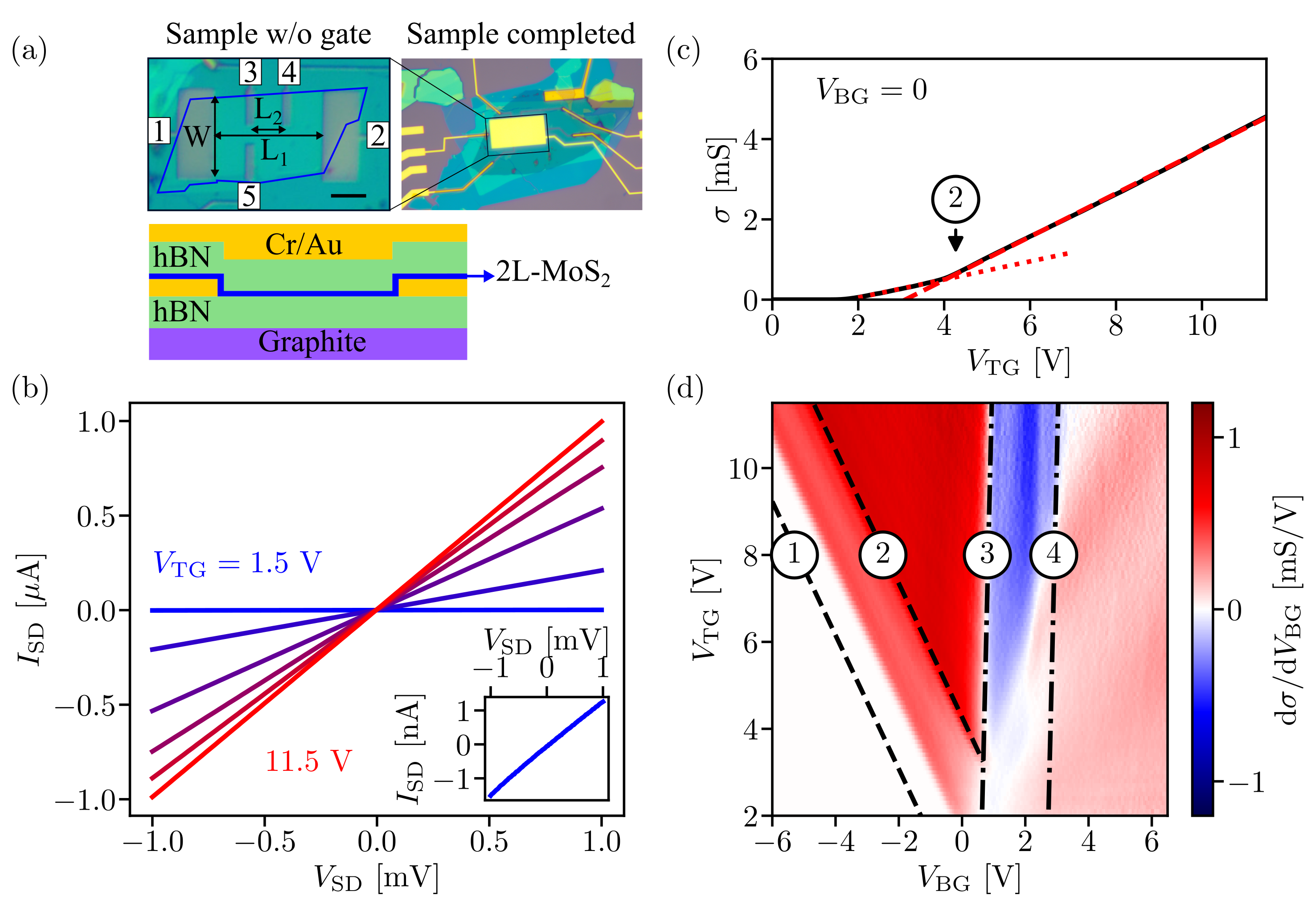
In this study, a bilayer MoS2 with dual-gated architecture is employed to study electron transport. Figure 1(a) shows optical images (upper panel) and a schematic side view (lower panel) of the device. The fabrication starts by assembling a thin hBN and graphite layers onto a silicon/silicon dioxide chip ( of oxide layer). The graphite serves as the bottom gate, while the hBN is the gate dielectric material. The layers are stacked together using a dry-transfer technique (see Refs. [21, 24, 25] for details). We pattern metallic contacts (Cr/Au: /) with standard electron beam lithography and electron beam evaporation. The region of the contacts is then cleaned thoroughly with the tip of an atomic force microscope in contact mode. This step is crucial to remove the residues of the lithography process. The bilayer MoS2 is obtained by mechanically cleaving a bulk MoS2 crystal from natural sources (SPI supply) and identified by optical contrast, which has proven to be a very reliable method [26, 27, 28, 29]. A second stack with a layer of hBN and the bilayer MoS2 is assembled, then aligned and deposited on top of the contacts. Both exfoliation and assembling take place in a glove box with argon atmosphere (). The metallic top gate is patterned with standard lithography processes and covers the entire MoS2 flake. In the final step, we vacuum anneal the sample at for to improve the contact interface. All measurements presented in this work (if not explicitly stated otherwise) are performed at a temperature of at low frequency () and low excitation voltage () with standard lock-in techniques.
First, we characterize the contacts to ensure Ohmic behavior and low contact resistance. The dc output characteristics are shown in Fig. 1(b) for different top gate voltages (). The two-terminal resistance changes from to as a function of . The current shows a linear dependence on the applied source-drain voltage down to the lowest (inset), indicating a vanishing Schottky barrier. The average contact resistance of source and drain contacts (1 and 2) is for and does not depend on the applied bottom gate voltage (). To the best of our knowledge, this is one of the lowest values reported in the literature and is comparable to bismuth contacts [30]. The vanishing Schottky barrier and the low contact resistance allow us to study electron transport at low densities (down to ) at low source-drain voltage ().
The four-terminal conductivity () as a function of is shown in Fig. 1(c). We identify two voltage ranges, where the conductivity features a linear dependence on , which differs by the slope. The two slopes of yield the mobilities (dotted line) and (dashed line). This specific shape of the four-terminal conductivity is a general property of high-quality single-gated MoS2 devices [see Fig. 1(c) in Ref. [20] and Fig. 1(d) in the supplemental material of Ref. [21] for a direct comparison]. The kink marked with the number 2 is related to the population of the upper spin-orbit (SO) split band, as will be demonstrated below.
Figure 1(d) shows the derivative of the conductivity as a function of and . For the dependence of the conductivity is monotonic and resembles its dependence. There are two distinct rates that are separated by a black dashed line (number 2). This line follows constant density conditions, separating the single band from the two-band regime. From this result, we conclude that the separation between the bands is not displacement field dependent (i.e., the SO gap is not tunable with the electric field). In contrast, for the dependence of the conductivity on is nonmonotonic. The conductivity features a local maximum (number 3) that is almost independent of . The origin of the negative is related to the population of the bottom layer and will be discussed in Sec. II.1.
So far we have characterized the field effect transistor at zero magnetic field. Understanding the contribution of the bands in multilayer MoS2 devices is an essential step for interpreting their electronic properties. In the following, we will demonstrate that all features observed in the conductivity can be attributed to the population of different bands in the MoS2 bilayer. To verify this hypothesis, we now turn our attention to magnetotransport measurements, from which we determine the electron density and the band occupation.
II.1 Band and layer occupation
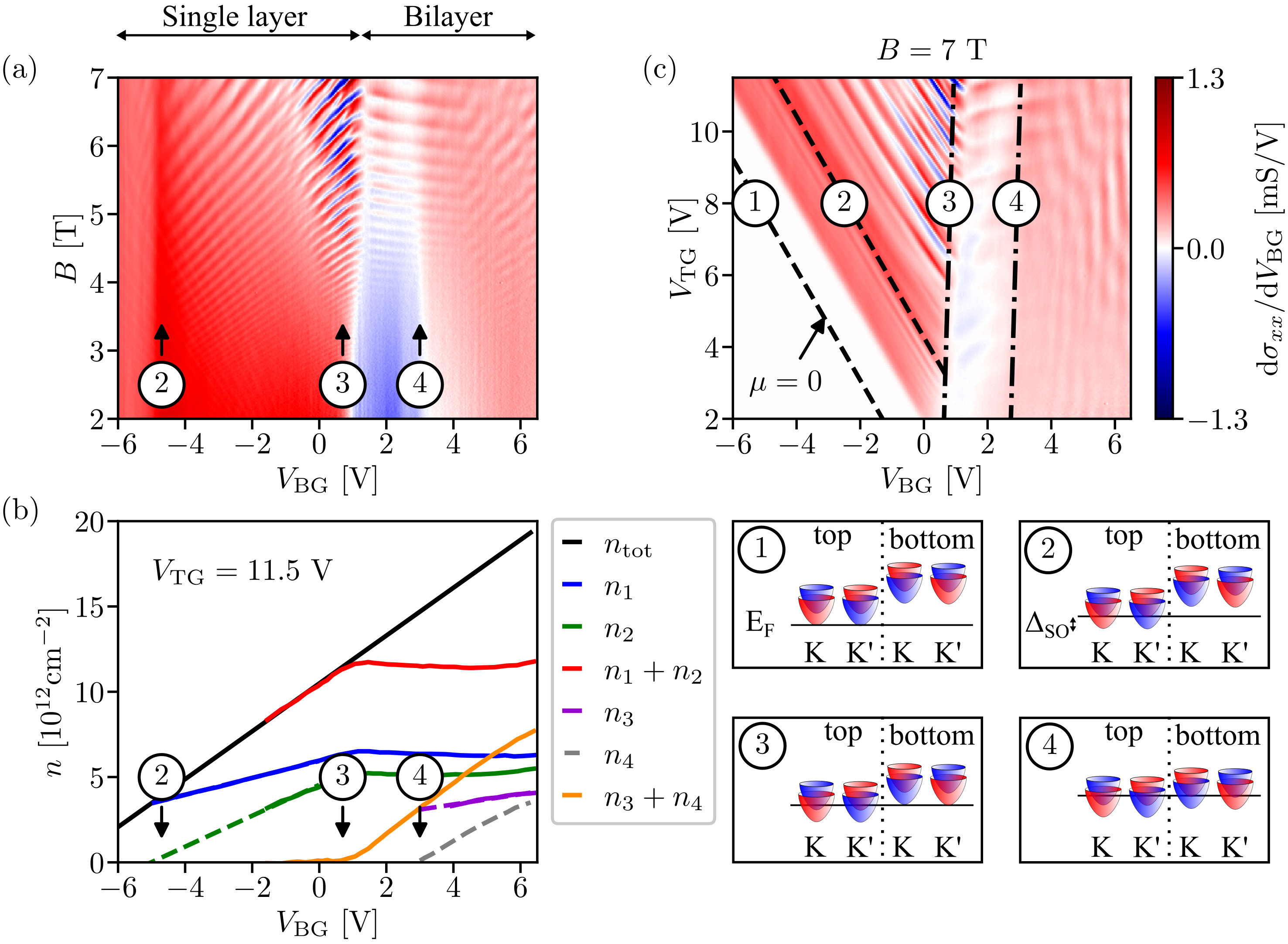
The aim of this part is to determine how the different bands are filled with electrons as we change the gate voltages. For this purpose we measure the magnetoconductivity , applying a perpendicular magnetic field . The conductivity is obtained by tensor inversion of the two-dimensional resistivity with components and . From the Shubnikov–de Haas oscillations (SdHO) we determine the density of band as we did in previous works [21, 24, 25]. The total density is given by
| (1) |
where and . The total density is related to the band densities via . We do not determine the total density from the Hall effect, because the contacts extend across most of the conducting channel, leading to an overestimation of the density.
Figure 2(a) shows the derivative of the magnetoconductivity as a function of and for . The conductivity features oscillations periodic in , as we expect for SdHO. From the Fourier spectrum of the (see Ref. [24, 25] for details) we determine the densities shown in Fig. 2(b). As in Ref. [24], we attribute a twofold valley degeneracy to each band , which accounts for the two valleys (see schematics in the lower right panel of Fig. 2). In the regime , where we find only two frequencies in the Fourier spectrum, there is remarkable agreement between the calculated and the experimentally defined density . In our interpretation, the densities and belong to the top MoS2 layer. In the regime , the density saturates, because the bottom MoS2 layer becomes conducting, screening the field effect of the bottom gate. This behavior is in complete agreement with the behavior found and explained in previous studies [24, 25].
The layer occupation can be controlled in dual-gated devices. For and only the top layer is occupied by electrons and we can tune between single- and double-band transport. The onset of (marked by the number 2) corresponds to the population of the upper SO split band of the top layer (see schematics of the band structure in Fig 2). To support this interpretation we determine the density that is required to start filling the upper SO split band. In an effective mass approximation, this density corresponds to an energy , in agreement with the value reported in Ref. [24].
Figure 2(c) shows at as a function of the voltage applied to the top and bottom gates. This measurement defines a phase diagram for the bilayer MoS2 that is divided into five different regimes by the dashed (dotted) lines. Each line indicates the onset of a specific band (from 1 to 4 increasing ). The bilayer is tuned from an insulating into a conducting phase, where up to four bands contribute to electron transport. In the remaining part of this paper, we focus on the narrow single-band transport regime enclosed by the dashed lines in Fig. 2(c).
II.2 Strong electron localization
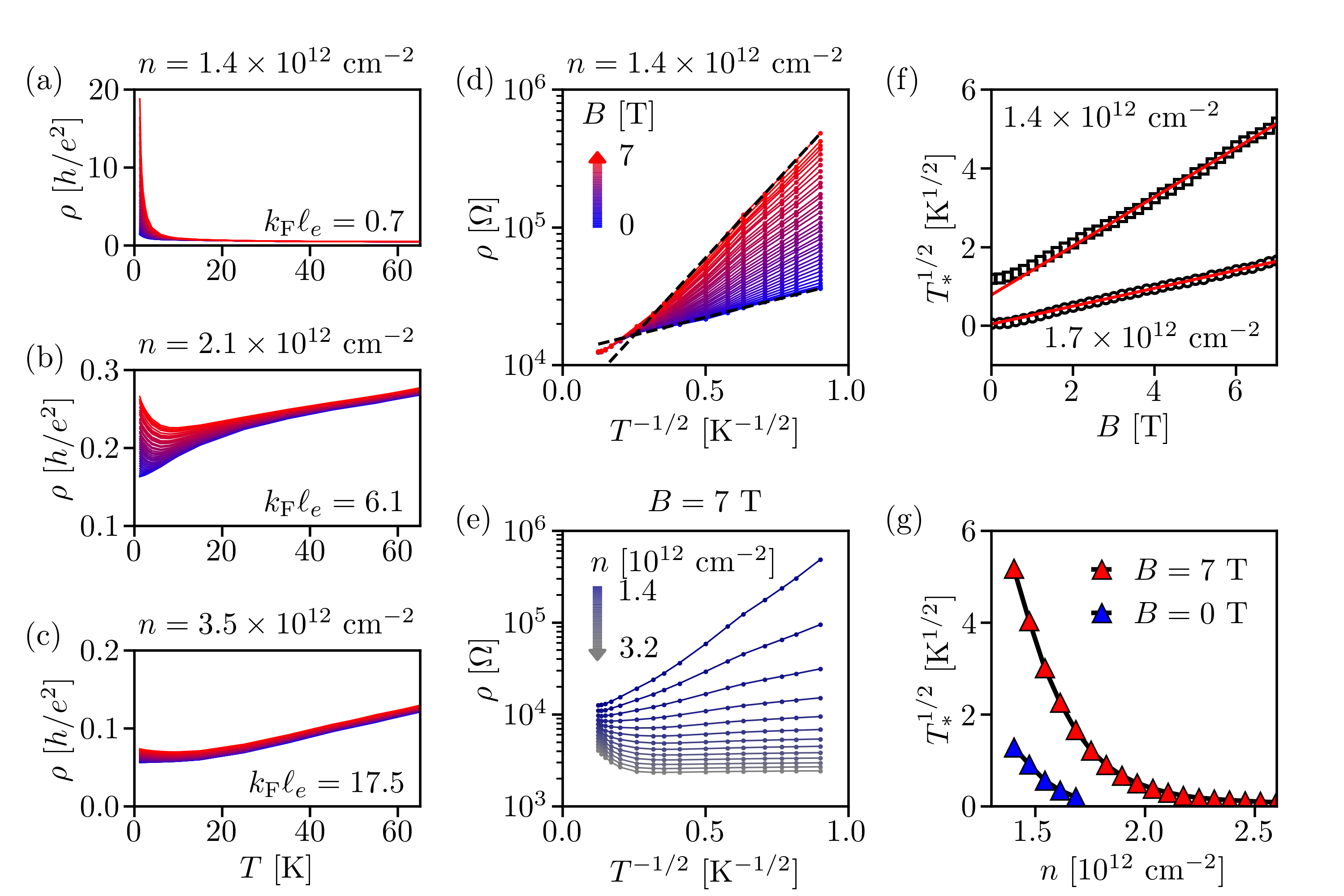
We now turn our attention to the magnetoresistance in the single-band transport regime. According to the Drude model, the longitudinal resistance does not depend on the magnetic field. However, we observe a non-saturating positive magnetoresistance in the low-density range (). The magnetoresistance increases by more than one order of magnitude at and , as shown in Figs. 3(a)–3(c). A qualitatively similar positive magnetoresistance was observed in monolayer MoS2 [31], where a negative magnetoresistance (due to weak localization) gradually turned into a positive magnetoresistance as the temperature and density were lowered. This effect was attributed to the transition from weak localization to weak anti-localization, despite the authors realizing that the shape of the magnetoresistance was not well described by the theory of weak antilocalization. Also, in another bilayer [32, 24] and three-layer MoS2 devices [25] a similar behavior has been observed but was not further investigated. The observation of a positive magnetoresistance in samples prepared and studied in different research groups suggests that there is a common origin for this effect. Owing to the relatively low electron mobility in MoS2 and the large intrinsic defect density [33], we consider the role of disorder [34] and electron localization to describe the nonsaturating positive magnetoresistance.
Figures 3(a)–3(c) show the four-terminal longitudinal resistivity as a function for three different densities (from ) and various magnetic fields. At zero magnetic field (violet curve) we observe a metal-insulator transition as we lower the density. It is remarkable that this transition occurs at relatively high densities , where the ratio between Coulomb and kinetic energy is still moderate . Therefore, the transition is more likely to be a manifestation of strong electron localization when the Fermi energy approaches the bottom of the conduction band, rather than an insulating state due to correlations. At the lowest temperature, we estimate the product () between Fermi wave vector () and electron mean free path (). Strong electron localization occurs for [as shown in Fig. 3(a)], while band conduction occurs for . Applying a perpendicular magnetic field breaks this condition, inducing a metal-insulator transition even for [see Fig. 3(b)].
The resistivity is plotted on a logarithmic scale as a function of in Fig. 3(d) for the lowest density and various magnetic fields. At low temperatures () all the curves follow a linear dependence, as predicted by the ES theory. The slope of the curves increases with increasing magnetic field. Therefore, we define a parameter that depends on the magnetic field, such that the resistivity is described by
This function seems to capture the temperature dependence of the resistivity for , while above this temperature the resistance shows a weaker temperature and magnetic field dependence. The parameter obtained from the fit is shown in Fig. 3(f). This parameter depends roughly linearly (at least above ) on the applied magnetic field and the slope decreases with increasing electron density. Similarly, we plot the resistivity for different densities [see Fig. 3(e)] and extrapolate the parameter as a function of densities. The density dependence of is shown in Fig. 3(g), where we see increasing rapidly for decreasing density.
We considered other models to describe our data, such as Mott’s law () and thermally activated nearest-neighbor hopping (). While thermally activated hopping clearly fails in describing the temperature dependence of the resistivity, we obtain reasonable fits also with Mott’s law, which yields a slightly larger least-mean-square error. Based on the temperature dependence of the resistivity, we cannot reliably distinguish between the two models because the resistivity does not change by several orders of magnitude. For this reason, we also consider the role played by the magnetic field.
At finite magnetic fields, the tails of the electron wave functions decay faster and the overlap between the localized wave functions decreases. This leads to a reduction of the tunneling probability and thus to an increase in the resistance. This effect results in an exponential increase of the resistance of the form [12]
where depends on the range of magnetic field and the assumptions made in the theoretical model [12, 35, 36].
First, we focus on the low magnetic field range (, being the magnetic length and the localization length), where the effect of can be treated as a small correction to . The low magnetic field correction of the percolation parameter is given by [37]
where is a numerical parameter, and . This expression yields the magnetoresistivity
| (2) |
which can be expanded in a quadratic expression for .
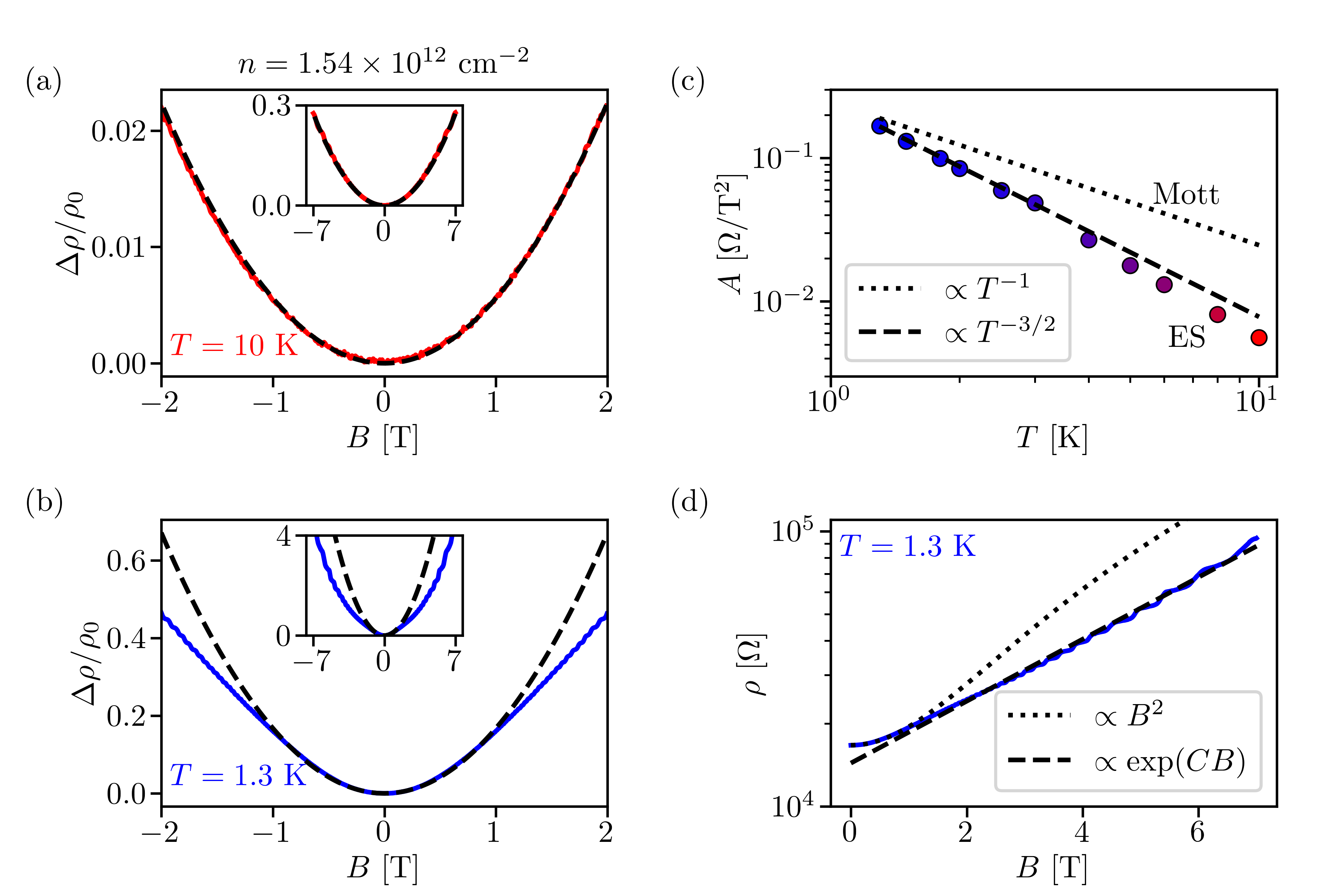
Figures 4(a) and 4(b) show the low magnetic field range of the resistivity at the density (i.e., below ) and for two exemplary temperatures. At the resistivity shows a quadratic dependence on , as predicted by Eq. (2). At this temperature, the model fits the data well in the entire magnetic field range probed in our experiments, as shown by the inset of Fig. 4(a). The range of magnetic field for which this model is able to describe the data shrinks with lowering the temperature because the parameter grows with lowering the temperature (), thus limiting the magnetic field range for which our approximation is valid. Therefore, it is not surprising that at [Fig. 4(b)] the model deviates from the data at where becomes a large correction.
Fitting the magnetoresistance at different temperatures provides the temperature dependence of the curvature, which is the only fitting parameter. The result of the fit is shown in Fig. 4(c) on a log-log scale for the density . The data follow the temperature dependence . For comparison, we show the temperature dependence () predicted by the Mott theory, which clearly deviates from the trend of our data, while the data are in good agreement with ES theory (). Based on this observation, we conclude that, in “diluted” MoS2, long-range Coulomb interactions lead to the formation of a gap in the density of states at the Fermi energy. This conclusion is further supported by the interaction parameter , which is modest but indicates that the Coulomb energy is significantly larger than the kinetic energy of free electrons.
At this point, we would like to discuss our quantitative results. By fitting the data with ES law we can estimate the localization length according to
| (3) |
where is the relative dielectric constant of MoS2, and is a numerical constant [37]. This equation, however, provides localization lengths of a few micrometers, which is surprisingly large considering the inter-particle spacing (). To verify the validity of this result, we estimate the localization length from the curvature of the magnetoresistance and compare the two results. By inserting (obtained from the temperature dependence) in the definition of we obtain at a density of . This result differs by more than one order of magnitude from the one obtained by Eq. (3).
Here, we offer an argument that might explain the discrepancy between these two results. We note that in our device the metallic gate is only separated from the 2D electron system by a thin hBN layer (). This distance is comparable to the interparticle distance . As a consequence, the metallic gate screens Coulomb interactions at large distances (), where the Coulomb potential becomes dipole-like (). The presence of the metal plate partially suppresses the Coulomb gap due to its screening effect [38, 39, 40, 41, 42, 43]. For small hopping distances the density of available states still has a gap, while for long hopping distances the density of states is constant. At lower temperatures, long-distance hopping becomes favorable and VRH is determined by the constant density of states (like in the Mott VRH). Therefore, it is expected that in the presence of a nearby metallic gate, there is a critical temperature
below which the system shows a transition from ES to the “screened” Mott VRH [41]. This VRH is different from the usual Mott VRH, which is characterized by a different density of states.
We estimate this temperature to be around by assuming , placing our system just below the transition temperature. In contrast, the hopping distance
is of the order of , thus still in the Coulomb gap regime. Therefore, it is not clear from these characteristic quantities in which regime our sample is. As we argued above, we cannot, based on the temperature dependence, clearly distinguish between ES and Mott VRH. Under this condition, Eq. (3) may not be valid, as we are close to the transition between the two hopping transport regimes. On the other hand, the magnetic field promotes electron localization and reduces the probability of long-range hopping (less overlap of wave function tails). As shown in Fig. 3(f), the magnetic field dependence of the fitting parameter is compatible with the wave-function shrinking effect. In addition, the curvature clearly establishes that at finite field VRH follows ES theory. For this reason, we consider our estimation of the localization length from the analysis shown in Fig. 4 to be valid, from which we estimate .
Finally, we consider the asymptotic limit at high magnetic fields (). The typical hopping distance is strongly reduced by the effect of the magnetic field and the typical hopping energy increases. As a consequence, the Coulomb gap might be negligible at high -fields, as proposed by Nguyen [37]. The resistivity is expected to follow the asymptotic behavior described by Eq. (4),
| (4) |
with being a temperature-dependent coefficient. This equation captures the temperature dependence of the resistivity at high magnetic fields. However, the resistivity seems to follow instead of Eq. (4), as shown in Fig. 4(d). Given the divergent susceptibility of MoS2 at low density [20], we speculate that the spin polarization might contribute in increasing the magnetoresistance. As it was reported in Ref. [44] the mechanism that provides an enhanced magnetoresistance is related to the blocking of hopping due to spin polarization. Disentangling spin from orbital effects requires in-plane magnetic fields. However, the in-plane magnetic field does not couple to the electron spins in the valleys of MoS2, because the spin is locked out-of-plane due to SO coupling [45, 20].
III Conclusion
The low-temperature resistivity of bilayer MoS2 undergoes a transition from metallic to insulating temperature dependence at a critical density . This density is one order of magnitude larger than in silicon metal-oxide-semiconductor field-effect transistors [46] and three orders of magnitude larger than in GaAs quantum wells [47, 48]. We attribute this transition to a disorder-induced transition in agreement with other metal-insulator-transition observed in disordered materials [46]. In fact, our observation is in line with the proposal of Klapwijk and Das Sarma [5], which states that the transition should be observed when the electron density is close to a few electrons per ionized impurity. The ionized impurities may be sulfur vacancies, which are known to have an inhomogeneous distribution with an average density of [49], thus the same order of magnitude as in our sample.
In the insulating phase, the resistance drops exponentially with increasing temperature, compatible with variable-range hopping. The limited temperature range considered in our experiments does not provide a conclusive distinction between Mott and Efros-Shklovskii laws. On the other end, the magnetic field dependence at low fields closely follows an Efros-Shklovskii law. The Coulomb gap is likely to appear in the density of states of MoS2, as the interaction parameter () suggests that Coulomb energy is the dominant energy scale. However, the presence of a nearby metallic gate could contribute to the suppression of the gap in the density of state at large distances () [39, 41, 42, 43]. Despite the screening effect, we observe the presence of the Coulomb gap by applying a perpendicular magnetic field. We interpret this result based on the wave function shrinking, which reduces long distant hopping.
Acknowledgments
We thank Boris Shklovskii, Hadrien Duprez, and David Kealhofer for fruitful discussions. We thank Peter Märki, Thomas Bähler, as well as the FIRST staff for their technical support. We acknowledge support from the European Graphene Flagship Core3 Project, Swiss National Science Foundation via NCCR Quantum Science, and H2020 European Research Council (ERC) Synergy Grant under Grant Agreement 95154. K.W. and T.T. acknowledge support from JSPS KAKENHI (Grants No. 19H05790, No. 20H00354, and No. 21H05233).
References
- Imada et al. [1998] M. Imada, A. Fujimori, and Y. Tokura, Metal-insulator transitions, Reviews of Modern Physics 70, 1039 (1998).
- Castellani et al. [1998] C. Castellani, C. Di Castro, and P. A. Lee, Metallic phase and metal-insulator transition in two-dimensional electronic systems, Physical Review B 57, R9381 (1998), publisher: American Physical Society.
- Phillips et al. [1998] P. Phillips, Y. Wan, I. Martin, S. Knysh, and D. Dalidovich, Superconductivity in a two-dimensional electron gas, Nature 395, 253 (1998), number: 6699 Publisher: Nature Publishing Group.
- Chakravarty et al. [1999] S. Chakravarty, S. Kivelson, C. Nayak, and K. Voelker, Wigner glass, spin liquids and the metal-insulator transition, Philosophical Magazine B 79, 859 (1999), publisher: Taylor & Francis _eprint: https://doi.org/10.1080/13642819908214845.
- Klapwijk and Das Sarma [1999] T. M. Klapwijk and S. Das Sarma, A few electrons per ion scenario for the B=0 metal–insulator transition in two dimensions, Solid State Communications 110, 581 (1999).
- Das Sarma and Hwang [1999] S. Das Sarma and E. H. Hwang, Charged Impurity-Scattering-Limited Low-Temperature Resistivity of Low-Density Silicon Inversion Layers, Physical Review Letters 83, 164 (1999), publisher: American Physical Society.
- Das Sarma [1995] S. Das Sarma, Screening and Many-Body Effects in Low-Dimensional Electron Systems, in Quantum Transport in Ultrasmall Devices: Proceedings of a NATO Advanced Study Institute on Quantum Transport in Ultrasmall Devices, held July 17–30, 1994, in II Ciocco, Italy, NATO ASI Series, edited by D. K. Ferry, H. L. Grubin, C. Jacoboni, and A.-P. Jauho (Springer US, Boston, MA, 1995) pp. 339–357.
- Shashkin and Kravchenko [2021] A. A. Shashkin and S. V. Kravchenko, Metal–insulator transition and low-density phases in a strongly-interacting two-dimensional electron system, Annals of Physics Special Issue on Localisation 2020, 435, 168542 (2021).
- Anderson [1958] P. W. Anderson, Absence of Diffusion in Certain Random Lattices, Physical Review 109, 1492 (1958), publisher: American Physical Society.
- Abrahams et al. [1979] E. Abrahams, P. Anderson, D. Licciardello, and T. Ramakrishnan, Scaling theory of localization: Absence of quantum diffusion in two dimensions, Physical Review Letters 42, 673 (1979).
- Shayegan [2022] M. Shayegan, Wigner crystals in flat band 2D electron systems, Nature Reviews Physics 4, 212 (2022), number: 4 Publisher: Nature Publishing Group.
- Shklovskii and Efros [1984] B. I. Shklovskii and A. L. Efros, Electronic Properties of Doped Semiconductors, edited by M. Cardona, P. Fulde, and H.-J. Queisser, Springer Series in Solid-State Sciences, Vol. 45 (Springer Berlin Heidelberg, Berlin, Heidelberg, 1984).
- Mott [1968] N. F. Mott, Conduction in glasses containing transition metal ions, Journal of Non-Crystalline Solids 1, 1 (1968).
- Pollak [1970] M. Pollak, Effect of carrier-carrier interactions on some transport properties in disordered semiconductors, Discussions of the Faraday Society 50, 13 (1970), publisher: The Royal Society of Chemistry.
- Ambegaokar et al. [1971] V. Ambegaokar, B. I. Halperin, and J. S. Langer, Hopping Conductivity in Disordered Systems, Physical Review B 4, 2612 (1971), publisher: American Physical Society.
- Efros and Shklovskii [1975] A. L. Efros and B. I. Shklovskii, Coulomb gap and low temperature conductivity of disordered systems, Journal of Physics C: Solid State Physics 8, L49 (1975), publisher: IOP Publishing.
- Radisavljevic and Kis [2013] B. Radisavljevic and A. Kis, Mobility engineering and a metal–insulator transition in monolayer MoS, Nature Materials 12, 815 (2013).
- Xue et al. [2019] J. Xue, S. Huang, J.-Y. Wang, and H. Q. Xu, Mott variable-range hopping transport in a MoS2 nanoflake, RSC Advances 9, 17885 (2019), publisher: The Royal Society of Chemistry.
- Moon et al. [2018] B. H. Moon, J. J. Bae, M.-K. Joo, H. Choi, G. H. Han, H. Lim, and Y. H. Lee, Soft Coulomb gap and asymmetric scaling towards metal-insulator quantum criticality in multilayer MoS2, Nature Communications 9, 2052 (2018), number: 1 Publisher: Nature Publishing Group.
- Lin et al. [2019] J. Lin, T. Han, B. A. Piot, Z. Wu, S. Xu, G. Long, L. An, P. Cheung, P.-P. Zheng, P. Plochocka, X. Dai, D. K. Maude, F. Zhang, and N. Wang, Determining Interaction Enhanced Valley Susceptibility in Spin-Valley-Locked MoS2, Nano Letters 19, 1736 (2019), publisher: American Chemical Society.
- Pisoni et al. [2018] R. Pisoni, A. Kormányos, M. Brooks, Z. Lei, P. Back, M. Eich, H. Overweg, Y. Lee, P. Rickhaus, K. Watanabe, T. Taniguchi, A. Imamoglu, G. Burkard, T. Ihn, and K. Ensslin, Interactions and Magnetotransport through Spin-Valley Coupled Landau Levels in Monolayer , Physical Review Letters 121, 247701 (2018).
- Smoleński et al. [2021] T. Smoleński, P. E. Dolgirev, C. Kuhlenkamp, A. Popert, Y. Shimazaki, P. Back, X. Lu, M. Kroner, K. Watanabe, T. Taniguchi, I. Esterlis, E. Demler, and A. Imamoğlu, Signatures of Wigner crystal of electrons in a monolayer semiconductor, Nature 595, 53 (2021), number: 7865 Publisher: Nature Publishing Group.
- Yoon et al. [1999] J. Yoon, C. C. Li, D. Shahar, D. C. Tsui, and M. Shayegan, Wigner Crystallization and Metal-Insulator Transition of Two-Dimensional Holes in GaAs at , Physical Review Letters 82, 1744 (1999), publisher: American Physical Society.
- Pisoni et al. [2019] R. Pisoni, T. Davatz, K. Watanabe, T. Taniguchi, T. Ihn, and K. Ensslin, Absence of Interlayer Tunnel Coupling of -Valley Electrons in Bilayer , Physical Review Letters 123, 117702 (2019).
- Masseroni et al. [2021] M. Masseroni, T. Davatz, R. Pisoni, F. K. de Vries, P. Rickhaus, T. Taniguchi, K. Watanabe, V. Fal’ko, T. Ihn, and K. Ensslin, Electron transport in dual-gated three-layer , Physical Review Research 3, 023047 (2021), publisher: American Physical Society.
- Ni et al. [2007] Z. H. Ni, H. M. Wang, J. Kasim, H. M. Fan, T. Yu, Y. H. Wu, Y. P. Feng, and Z. X. Shen, Graphene Thickness Determination Using Reflection and Contrast Spectroscopy, Nano Letters 7, 2758 (2007), publisher: American Chemical Society.
- Li et al. [2012] H. Li, G. Lu, Z. Yin, Q. He, H. Li, Q. Zhang, and H. Zhang, Optical Identification of Single- and Few-Layer Sheets, Small 8, 682 (2012).
- Yang et al. [2013] H. Yang, H. Hu, Y. Wang, and T. Yu, Rapid and non-destructive identification of graphene oxide thickness using white light contrast spectroscopy, Carbon 52, 528 (2013).
- Bing et al. [2018] D. Bing, Y. Wang, J. Bai, R. Du, G. Wu, and L. Liu, Optical contrast for identifying the thickness of two-dimensional materials, Optics Communications Optoelectronics and Photonics Based on Two-dimensional Materials, 406, 128 (2018).
- Shen et al. [2021] P.-C. Shen, C. Su, Y. Lin, A.-S. Chou, C.-C. Cheng, J.-H. Park, M.-H. Chiu, A.-Y. Lu, H.-L. Tang, M. M. Tavakoli, G. Pitner, X. Ji, Z. Cai, N. Mao, J. Wang, V. Tung, J. Li, J. Bokor, A. Zettl, C.-I. Wu, T. Palacios, L.-J. Li, and J. Kong, Ultralow contact resistance between semimetal and monolayer semiconductors, Nature 593, 211 (2021), number: 7858 Publisher: Nature Publishing Group.
- Schmidt et al. [2016] H. Schmidt, I. Yudhistira, L. Chu, A. Castro Neto, B. Özyilmaz, S. Adam, and G. Eda, Quantum Transport and Observation of Dyakonov-Perel Spin-Orbit Scattering in Monolayer MoS 2, Physical Review Letters 116, 046803 (2016).
- Papadopoulos et al. [2019] N. Papadopoulos, K. Watanabe, T. Taniguchi, H. S. J. van der Zant, and G. A. Steele, Weak localization in boron nitride encapsulated bilayer , Physical Review B 99, 115414 (2019), publisher: American Physical Society.
- Rhodes et al. [2019] D. Rhodes, S. H. Chae, R. Ribeiro-Palau, and J. Hone, Disorder in van der Waals heterostructures of 2D materials, Nature Materials 18, 541 (2019), number: 6 Publisher: Nature Publishing Group.
- Ahn and Das Sarma [2022] S. Ahn and S. Das Sarma, Disorder-induced two-dimensional metal-insulator transition in moiré transition metal dichalcogenide multilayers, Physical Review B 105, 115114 (2022), publisher: American Physical Society.
- Mikoshiba [1962] N. Mikoshiba, Strong-Field Magnetoresistance of Impurity Conduction in -Type Germanium, Physical Review 127, 1962 (1962), publisher: American Physical Society.
- Ioffe and Spivak [2013] L. B. Ioffe and B. Z. Spivak, Giant magnetoresistance in the variable-range hopping regime, Journal of Experimental and Theoretical Physics 117, 551 (2013).
- Nguyen Van Lien [1995] Nguyen Van Lien, Crossovers in two-dimensional variable range hopping, Physics Letters A 207, 379 (1995).
- Aleiner and Shklovskii [1994] I. L. Aleiner and B. I. Shklovskii, Effect of screening of the Coulomb interaction on the conductivity in the quantum Hall regime, Physical Review B 49, 13721 (1994), publisher: American Physical Society.
- Cuevas et al. [1994] E. Cuevas, M. Ortuño, J. Ruiz, V. Gasparian, and M. Pollak, Electrode screening of the Coulomb gap, Philosophical Magazine B 70, 1231 (1994), publisher: Taylor & Francis _eprint: https://doi.org/10.1080/01418639408240286.
- Pikus and Efros [1995] F. G. Pikus and A. L. Efros, Coulomb gap in a two-dimensional electron gas with a close metallic electrode, Physical Review B 51, 16871 (1995), publisher: American Physical Society.
- Hu et al. [1995] X. L. Hu, F. W. Van Keuls, Y. Carmi, H. W. Jiang, and A. J. Dahm, Screening of the Coulomb gap, Solid State Communications 96, 65 (1995).
- Van Keuls et al. [1997] F. W. Van Keuls, X. L. Hu, H. W. Jiang, and A. J. Dahm, Screening of the Coulomb interaction in two-dimensional variable-range hopping, Physical Review B 56, 1161 (1997), publisher: American Physical Society.
- Ho et al. [2010] L. H. Ho, A. P. Micolich, W. R. Clarke, O. Klochan, and A. R. Hamilton, The Reduced Effective Interaction Parameter in Closely Spaced Two‐dimensional Hole Systems, AIP Conference Proceedings 1199, 209 (2010), publisher: American Institute of Physics.
- Meir [1996] Y. Meir, Universal spin-induced magnetoresistance in the variable-range hopping regime, Europhysics Letters 33, 471 (1996), publisher: IOP Publishing.
- Movva et al. [2017] H. C. Movva, B. Fallahazad, K. Kim, S. Larentis, T. Taniguchi, K. Watanabe, S. K. Banerjee, and E. Tutuc, Density-Dependent Quantum Hall States and Zeeman Splitting in Monolayer and Bilayer, Physical Review Letters 118, 247701 (2017).
- Tracy et al. [2009] L. A. Tracy, E. H. Hwang, K. Eng, G. A. Ten Eyck, E. P. Nordberg, K. Childs, M. S. Carroll, M. P. Lilly, and S. Das Sarma, Observation of percolation-induced two-dimensional metal-insulator transition in a Si MOSFET, Physical Review B 79, 235307 (2009), publisher: American Physical Society.
- Simmons et al. [1998] M. Y. Simmons, A. R. Hamilton, M. Pepper, E. H. Linfield, P. D. Rose, D. A. Ritchie, A. K. Savchenko, and T. G. Griffiths, Metal-Insulator Transition at in a Dilute Two Dimensional GaAs-AlGaAs Hole Gas, Physical Review Letters 80, 1292 (1998), publisher: American Physical Society.
- Manfra et al. [2007] M. J. Manfra, E. H. Hwang, S. Das Sarma, L. N. Pfeiffer, K. W. West, and A. M. Sergent, Transport and Percolation in a Low-Density High-Mobility Two-Dimensional Hole System, Physical Review Letters 99, 236402 (2007), publisher: American Physical Society.
- Vancsó et al. [2016] P. Vancsó, G. Z. Magda, J. Pető, J.-Y. Noh, Y.-S. Kim, C. Hwang, L. P. Biró, and L. Tapasztó, The intrinsic defect structure of exfoliated single layers revealed by Scanning Tunneling Microscopy, Scientific Reports 6, 29726 (2016), number: 1 Publisher: Nature Publishing Group.