The Acoustophotoelectric Effect: Efficient Phonon–Photon–Electron Coupling in Zero-Voltage-Biased 2D SnS2 for Broadband Photodetection
Abstract
Two-dimensional (2D) layered metal dichalcogenides constitute a promising class of materials for photodetector applications due to their excellent optoelectronic properties. The most common photodetectors, which work on the principle of photoconductive or photovoltaic effects, however, require either the application of external voltage biases or built-in electric fields, which makes it challenging to simultaneously achieve high responsivities across broadband wavelength excitation—especially beyond the material’s nominal band gap—while producing low dark currents. In this work, we report the discovery of an intricate phonon–photon–electron coupling—which we term the acoustophotoelectric effect—in SnS2 that facilitates efficient photodetection through the application of 100-MHz-order propagating surface acoustic waves (SAWs). This effect not only reduces the band gap of SnS2, but also provides the requisite momentum for indirect band gap transition of the photoexcited charge carriers, to enable broadband photodetection beyond the visible light range, whilst maintaining pA-order dark currents—remarkably without the need for any external voltage bias. More specifically, we show in the infrared excitation range that it is possible to achieve up to eight orders of magnitude improvement in the material’s photoresponsivity compared to that previously reported for SnS2-based photodetectors, in addition to exhibiting superior performance compared to most other 2D materials reported to date for photodetection.
keywords:
Acoustophotoelectric effect, acoustophotocurrent, surface acoustic waves, tin disulfide, photodetectionA_SnS2_SI_ACS_Nano_clean \alsoaffiliationDepartment of Electrical and Electronic Engineering, The University of Melbourne, Parkville, VIC 3010, Australia \alsoaffiliationARC Centre of Excellence for Transformative Meta-Optical Systems, The University of Melbourne, VIC 3010, Australia
Two-dimensional (2D) layered metal chalcogenides have drawn significant attention for optoelectronic applications due to their excellent electronic and optical properties.1, 2 Specifically, 2D group IV metal chalcogenides have emerged as strong candidates for photodetectors because of their high absorption coefficient and relatively narrow band gap.3, 4, 5 A number of mechanisms exist by which the absorbed light is converted to electrical signals in these 2D materials, the most common of these being based on photoconductive and photovoltaic effects.6 While photodetectors based on the photoconductive mechanism can be constructed from a single monolithic material, they require an external DC bias for transfer of the photoexcited charge carriers, resulting in high dark currents, which lower their detectivity. On the other hand, photovoltaic photodetectors are based on heterostructures of p–n junctions with built-in electric fields such that an external DC bias is not required. As such, they produce lower dark currents, but nevertheless involve more complex architectures and suffer from lower responsivities due to their limited active areas.7 In addition, the photodetection range is limited by the band gap of the materials used. Therefore, a single-material photodetector that is capable of generating low dark currents while maintaining large responsivity, along with the ability to detect broadband illumination beyond the material’s nominal band gap, would be of significant interest.8
Recently, SnS2,9 which is an earth-abundant and environmentally-friendly intrinsic n-type semiconductor possessing a relatively wide band gap (2.1–2.8 eV)10, 11 and high absorption coefficient (104 cm-1),12 has shown considerable promise for nanoelectronics,13, 14, 15 and, in particular, photodetectors,16, 10, 17, 14, 18, 19, 20, 21, 22, 23, 24, 25, 26, 27, 28, 29, 30, 31, 32 even in comparison to other 2D materials such as MoS2 and WS2.24, 27 In order to improve its photodetection performance, various strategies have been explored, including the application of gate voltages,20, 19, 33 chemical doping,23, 25, 29 sensitization with PbS quantum dots,22 oxygen plasma treatment,27 surface coating,24 alloy engineering,34, 35 vacuum operation,17, 20, 18 and heterojunction formation.26, 31 Among these, chemical doping has been shown to facilitate considerable performance improvements in SnS2-based photodetectors. Such schemes however commonly involve the use of aggressive chemical or electrochemical processes that result in poor stability,25 in addition to irreversibly deteriorating the crystal structure by introducing defects into the material,36 although some doping techniques may not be suitable for wafer-scale 2D semiconductors.27 Moreover, it is important to note that SnS2, as with many other semiconductors, is not expected to produce photocurrents when excited by wavelengths with lower energies than its nominal band gap.28 Furthermore, given that SnS2 is an indirect semiconductor, an additional momentum source is required, usually in the form of phonon energy, to facilitate the indirect transition across the valence and conduction bands.1 As such, SnS2-based photodetectors, as well as most other photodetectors based on other 2D materials, have been limited to date to operation in the visible region; operation at wavelengths beyond 600 nm, where they exhibit very low photoresponsivities, have therefore rarely been reported.28
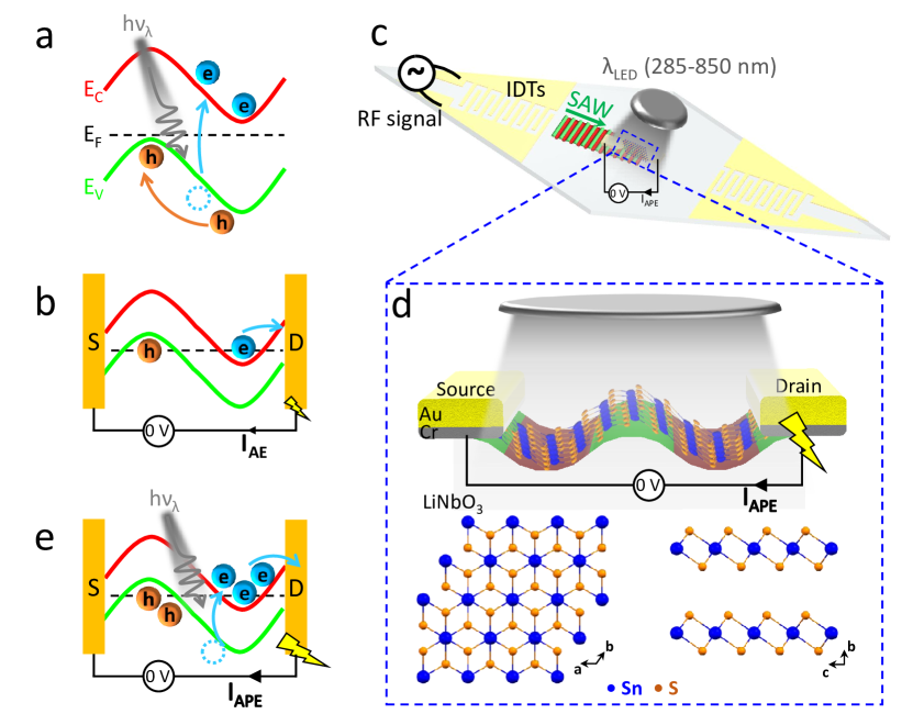
An alternative approach that we postulate could improve the photoresponsivity of SnS2, while maintaining its pristine condition, is through the use of MHz-order electromechanical coupling in the form of surface acoustic waves (SAWs)—nanometer-amplitude electromechanical waves that are generated on a single-crystal piezoelectric substrate, which have found application in telecommunication devices, superconducting circuits and acoustofluidics, among others.37, 38, 39 In addition to their demonstration as an efficient means for the synthesis and manipulation of 2D transition metal dichalcogenides and carbides/nitrides,40, 41, 42, 43, 44, 45 SAWs have also been shown to facilitate the control and manipulation of charge carriers in nanostructures.46, 47, 48 Broadly, SAWs have been used to either (i) manipulate photoexcited charge carriers in 2D semiconductors, to prevent their recombination and therefore allow their transfer over long distances (Fig. 1a),49, 50, 51 or, (ii) to enhance the electrical output in non-photoexcited 2D systems (Fig. 1b).46, 52, 53, 54, 55, 56, 57, 58, 59, 60, 61 The latter effect arises as a consequence of the native SAW electromechanical coupling that facilitates interaction of the wave with the mobile carriers. In a two-dimensional electron system (2DES), for example, this interaction has been shown to alter the SAW velocity and attenuate the wave intensity.46 The momentum from the wave is then transferred as a force onto the 2DES—a phenomenon known as the acoustoelectric (AE) effect, which has been investigated for a variety of other materials, including GaAs,46, 52 InGaAs,53 AlGaAs/GaAs heterojunctions,54, 55 single-walled carbon nanotubes,56 graphene,57, 58, 59 black phosphorus (BP),60 and MoS2.61 However, enhancement in carrier mobility due to the intricate tripartite coupling of phonons, photons and electrons in a photoexcited 2D material under the influence of the SAW has yet to be explored.
In this work, we report the discovery of unique phonon–photon–electron interactions, which we refer to as the acoustophotoelectric effect, that arises when the SAW is coupled into a 2D photoexcited SnS2 nanoflake on a piezoelectric substrate (Fig. 1(c,d)). Such an effect is observed to dramatically enhance the photocurrent output while operating at 0 V external DC bias, yielding a very low pA-order dark current and high photoresponsivity over a broad range of illumination wavelengths from the ultraviolet through to near-infrared regions. Moreover, the acoustophotoelectric effect not only lowers the nominal band gap of SnS2 from 2.3 to 1.4 eV, as confirmed by density functional theory (DFT) calculations, but also provides the requisite momentum to effect indirect transition of charge carriers into the conduction band, thereby extending photodetection capability considerably beyond the nominal band gap of SnS2 (approx. 550 nm). Specifically, photoresponsivities up to eight orders of magnitude higher than those of SnS2-based photodetectors reported in the literature were achieved in the infrared excitation range. We show too that thinner SnS2 flakes (approx. (10 nm)) exhibit larger acoustophotoelectric effect and hence acoustically-induced photoresponsivity values compared to thicker ones (approx. (100 nm)), across all wavelengths excitations across the UV, visible, and infrared ranges. This can be attributed to the enhanced acoustophotoelectric effect due to larger phonon–photon–electron coupling as a result of the material’s higher innate piezoelectricity (as inferred from its electromechanical coupling coefficient, ) in thinner films that lead to more efficient interactions between the SAW and the charge carriers in the material. With thicker films, however, the weaker coupling of the SAW into the material results in a diminished acoustophotoelectric effect. In addition, we briefly demonstrate that a similar acoustophotoelectric effect can be induced in other 2D materials, including MoS2 and SnS, therefore highlighting the promise of this technique as a practical, reversible, and non-destructive approach to significantly improve the performance of photodetectors based on 2D nanomaterials.
1 Results and Discussion
Although the focus of the present work encompasses the interplay between the electromechanical coupling of the SAW with a photoexcited material, i.e., the acoustophotoelectric effect, we first begin by baselining our observations of the electric current produced under the acoustic forcing but in the absence of light excitation, i.e., the acoustoelectric effect; these results will therefore be used as the control case to benchmark the results obtained for the photoexcited cases. Parenthetically, we note though that while the acoustoelectric effect has previously been reported in other 2D materials, such as graphene 62, 63, 57, 58, 59 GaAs,46 black phosphorus,60 and MoS2,61 it has not been demonstrated to date in any group IV A metal dichalcogenides.
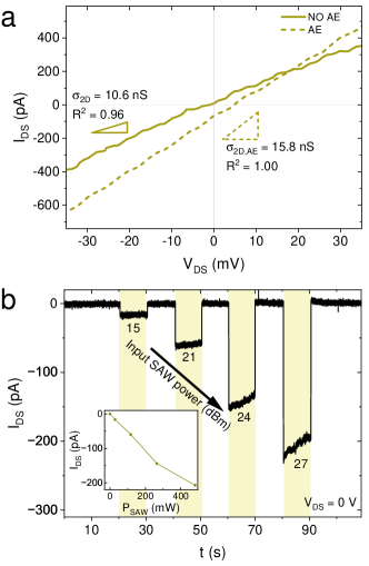
Figure 2a shows the current–voltage characteristics of a pristine (as verified from the x-ray photoelectron spectra (XPS) in Fig. S1) SnS2 nanoflake with thickness 48.7 1.3 nm (Fig. S2; considering a monolayer to be 0.6 nm thick, we estimate the flake to be composed of around 80 layers),64, 9 from which we calculate the flake’s conductivity to be 10.6 nS. The linearity in the profile over the -30 to 30 mV applied voltage range verifies the good Ohmic contact between the flake and the Cr/Au electrical contact pads.14, 20, 21, 33, 25, 29 Upon excitation of the SAW, it can be seen that the conductivity increases to 15.8 nS due to the momentum transfer from the acoustic waves to the charge carriers. 57 More importantly, the application of the SAW can be seen to generate an offset acoustoelectric current of 79.5 pA at V.
The transient acoustoelectric response of the SnS2 nanoflake to the SAW, obtained by cycling the SAW over four input powers from 15 to 27 dBm in 10 s on/off intervals with V, is plotted in Fig. 2b. It can be seen that the acoustoelectric current increases with increasing SAW power (see the inset of Fig. 2b), consistent with that predicted by the Weinreich equation65, 46, 66 (Equation S.1 in the Supplementary Information) together with the mobility of SnS2, calculated from the transfer curves in Fig. S3. For example, for a given input SAW power of 21 dBm, the theoretically estimated current is 210 pA, which is the same order of the experimental value of 60 pA (obtained from Fig. 2b).
In contrast, it can be seen from Fig. 3a that a significantly larger current is produced when the SnS2 nanoflake is illuminated with light (365 nm), even in the absence of the SAW excitation (-20 nA at -30 mV bias compared with -600 pA in the absence of light), attesting to the strong photosensitivity of SnS2,24, 14 which we note is the strongest under 285 and 365 nm illumination. The photosensitivity of SnS2 can be attributed to the commonly known photoconductive effect in which photon absorption in a semiconducting material results in the generation of excess free carriers, thereby leading to an increase in conductivity (i.e., the slope of the – curve). A further indication of the transport of photoinduced charge carriers over the electrical contact barriers is also evident from the linearity of the curves. 10
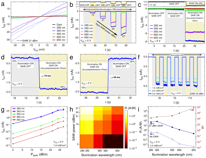
When excited with the SAW, however, we observe a significant offset in the – profile for the same illumination wavelength (365 nm) and intensity (3.0 mW/cm2), resulting in a current output of -8 nA at zero-bias voltage (Fig. 3a; cf. -0.1 nA in the absence of the SAW). To further probe the effect of the acoustic coupling, we turn to the current–time (–) measurements conducted at zero DC bias in Fig. 3b, wherein the nanoflake is again excited by incrementally increasing SAW powers within 10 s on/off periods, but in the presence of light illumination at different wavelengths. In distinct contrast to the case where the SAW is not present, we see giant enhancements in the photocurrent (, wherein , and denote the illumination wavelength, and the collected current in the presence and in the absence of light excitation, respectively) output due to the SAW, which can be more evidently seen in Fig. 3c. For comparison, the photocurrent under an illumination wavelength of 365 nm with an intensity of 3.0 mW/cm2 is only 135 pA, whereas excitation of the nanoflake with the SAW at 21 dBm input power yields 7.8 nA—an enhancement of almost two orders of magnitude. Importantly, this acoustophotoelectric current is also much larger than the acoustoelectric current, in the absence of light excitation of 60 pA, with the same SAW power (top panels in Fig. 3b,c), alluding to the stronger current generation capacity of the acoustophotoelectric effect over both the typical photoconductive and acoustoelectric effects.
To verify that the observed acoustophotoelectric current did not arise from the substrate itself, we conducted the same experiment on bare LiNbO3 in the absence of the SnS2 flake, in which no change in conductivity was observed (Fig. S4a) or electrical current produced (Fig. S4b).
Additionally, it is also possible to rule out the contribution of thermally-generated currents, particularly given that the relatively low applied SAW power over short durations (10 s) did not lead to appreciable temperature rises. Prolonged exposure to the SAW at 27 dBm over 30 s yielded a temperature rise in the substrate of only 0.5 ∘C, with no observable changes in the acoustophotoelectric current at 365 nm illumination. In any case, we note that the thermoelectric performance of SnS2 is typically hindered by intrinsically low carrier concentrations as a consequence of the material’s large band gap and high thermal conductivity.67
We further observe that the SnS2 nanoflake responds to the SAW excitation with rise and fall times of 79 and 69 ms, respectively, as can be seen from Fig. 3d,e. Moreover, a study of the electrical stability of the nanoflake subject to multiple SAW excitation cycles under illumination (Fig. 3f) indicated no significant deterioration to its performance, at least up to 6 cycles. We note that the acoustophotoelectric effect observed here is not just limited alone to SnS2. Similar observations were evident in other 2D materials, for example, MoS2 and SnS (see Fig. S5a,b), therefore alluding to the generality of the phenomenon.
An understanding of how the SAW interacts with the photoexcited carriers is nevertheless crucial to elucidate the underlying mechanisms responsible for the acoustophotoelectric effect. Typically, upon illumination of a semiconducting material, the charge carriers are excited from the valence band (EV) to the conduction band (EC), following which they tend to recombine to generate a photoluminescent (PL) signal. It is nevertheless well-known that SAWs are able to prevent the recombination of charge carriers, and quench the photoluminescence in semiconducting materials (Fig. 1a), as has been previously reported, for example, in MoS2,50, 68 WSe2,51 GaAs,69, 47, 70, 71 and InGaAs/GaAs.72 Similar PL quenching and spectrum broadening was observed here for the representative SnS2 nanoflake (Fig. S6), even beyond its nominal band gap up to 800 nm, thus indicating an alteration of the band structure in the material. In the absence of light excitation, and when a source and drain are present (Fig. 1b), the transfer of momentum from the SAW to the fast conduction electrons generates an acoustoelectric current 73 (Eqn. S.1 (Supplementary Information)), as has been shown for graphene and other 2D materials.46, 58, 61, 60 On illumination, however, the photoexcited charge carriers are raised to the conduction band that is altered by the SAW (Fig. 1e), where they accumulate and are transported to the drain. This tripartite phonon–photon–electron coupling is then responsible for the generation of the acoustophotoelectric current, thereby nullifying the need for an external DC bias that inevitably increases the dark currents. This is in contrast to typical photoconductors, where an external DC bias across the source and drain is required to collect the photocurrent. This can, for example, be seen in Fig. S7 where in the absence of the SAW, a large dark current of 20 nA is introduced with 1 V applied DC bias. Moreover, long rise and fall times (tens of seconds) can be seen, and little to no change in photocurrent is observed when the SnS2 nanoflake is excited at longer wavelengths (e.g., 850 nm). In stark contrast, we observe in Fig. 3g low (pA-order) dark currents as well as an increase in the acoustophotoelectric current for all illumination wavelengths, and especially beyond the SnS2 nominal band gap at 565, 660 and 850 nm, even without an applied DC bias.
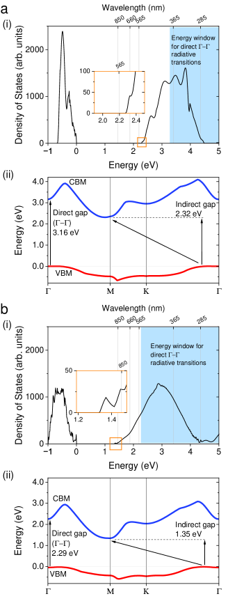
Further insight into the acoustophotoelectric enhancement of the current can be gleaned from density functional theory (DFT) simulations74, 75 (see Methods section) of the effect of the electromechanical coupling afforded by the SAW on the electronic properties of a 20 nm SnS2 (defect-free) thin film. The SAW is approximated in the simulations as combined electric ( ( V/m)) and mechanical strain (%) fields corresponding to that estimated for the 27 dBm SAW from the experiments. Figure 4 shows the resultant band structure (BS) and total electronic density of states (eDOS) for the case in which the strain and externally applied field are absent (Fig. 4a(i,ii)) and that for an applied external electric field of V/m and strain of 0.1% associated with that for 27 dBm SAW power in the experiments (Fig. 4b(i,ii)). A comparison between these plots allows us to conjecture that the electromechanical coupling arising from the SAW enhances the photocurrent at all illumination wavelengths by lowering the band gap (initially 2.32 eV; indirect) in the absence of SAW excitation, as seen from the BS plot in Fig. 4a (which is in good agreement with the experimental optical band gap calculated from the Tauc plot in Fig. S8), consistent with that observed in Fig. 3g.
To elaborate, it is expected that the degree of photocurrent enhancement is dependent on whether the illumination wavelength corresponds to an energy region for which indirect or direct radiative transition can occur. Both Figs. 4 and S8 show that SnS2 is a semiconductor with an indirect band gap, i.e., it possesses energies lower than the threshold for direct radiative transitions. The enhancement in photocurrent at 285 and 365 nm can be attributed to the efficient transport of the photoexcited carriers since the photon energy is already deeper within the conduction band region, thereby permitting direct radiative transition to occur. For longer wavelength excitation and in contrast to direct semiconductors, additional phonons are required for conservation of energy and crystal momentum in indirect semiconductors; as such, indirect semiconductors usually require larger momentum transfer to effect indirect transitions.76, 1, 77 Since such transitions involve a two-step process and are strongly dependent on the phonon density of states, the rate at which these transitions occur are typically much slower than those for direct transitions.78 Nevertheless, we see from Fig. 4b that even though the photon energy at 565 nm is below that for direct (–) radiative transition, detailed analysis of the band structure shows that direct radiative transition is possible along the –M path of the Brillouin zone due to the effect of the SAW in lowering the band gap of the SnS2 thin film from 2.32 eV down to 1.35 eV. As such, the enhancement in the photocurrent due to the applied SAW at 565 nm can be attributed to the fact that the photon energy is now sufficient for direct –), as opposed to indirect, transition.
We should note that although band gap tuning of semiconductors has been achieved to date through the application of a static transverse electric field via the Franz–Keldysh and Stark effects, the change in the band gap that has been demonstrated through these methods has been confined to only a few hundred meV and at the extra cost of patterning complex electrode structures to include physical top and bottom gates.79 The application of the SAW here therefore not only offers a facile means by which electrode-free electric field perturbation with associated directional strain can be imposed on the material, but also facilitates considerably larger changes in the band gap, in addition to providing the required momentum for indirect transitions.
In the present case of SnS2, the indirect band gap is lowered by 0.97 eV, so much so that the electromechanical coupling of the SAW into the SnS2 thin film not only provides the momentum required for the generation of the acoustophotoelectric current but also for the photoexcitation of the charge carriers to be extended to illumination wavelengths up to 850 nm.
To contrast the acoustophotoelectric effect observed with the SAW with the typical photoconductive effect that has been discussed to date, we examined the SnS2 film under different illumination wavelengths from 285 to 850 nm with 1 V applied DC bias in the absence of the SAW excitation. As can be seen in Fig. S7, high photocurrent values are obtained but at the expense of higher dark currents and much longer response times, the latter due to the slow generation of electron–hole pairs.27 The eDOS and BS plots for SnS2 in the absence of the SAW excitation (Fig. 4a) confirm the stronger photocurrent response at 285 and 365 nm since direct radiative transitions occur at these photon energies in comparison with the weaker response at 565 nm where the energy becomes sufficient to permit indirect transitions. At 660 nm, below the band gap in Fig. 4a, we nevertheless observe a very weak photocurrent in the experiments (although this could possibly arise due to defects in the thin film, which could introduce defect states and assist the absorption of photons with energies lower than the intrinsic band gap27) whereas poor photosensitivity was observed at 850 nm, even in the presence of the 1 V DC bias.
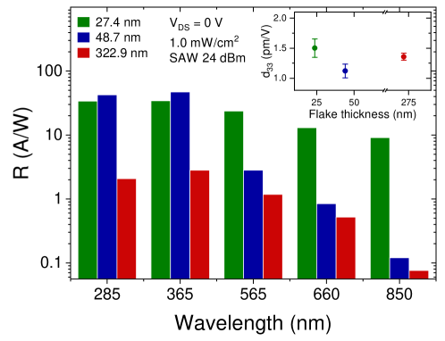
Finally, to demonstrate the utility of the platform in enhancing the photodetection performance of SnS2, we measure the important figure of merit qualities of photodetectors, including the dark current, photoresponsivity (, in which , , and constitute the responsivity under an illumination wavelength , the illumination intensity, and the active area of the photodetector, respectively), external quantum efficiency EQE, noise equivalent power NEP (calculated from the noise characteristics plots in Fig. S9), specific detectivity , and response times (see calculation methods for each parameter in the photodetector characterization section in the Supplementary Information). Values for the dark current extracted from the – plots in Fig. 3b are tabulated in Table S1, from which we note their pA-order magnitude across the cases examined—an advantage of operating without an external DC bias, which results in lower noise levels and higher ,80 in addition to minimizing quiescent power.81 As can be seen from Fig. 3g,h, both the acoustophotocurrent as well as the photoresponsivity are dramatically enhanced with increasing SAW input powers up to 365 A/W at 27 dBm. For the longer illumination wavelengths (565, 660, and 850 nm), we note that the decrease in the band gap due to the electric and strain fields produced by the SAW electromechanical coupling into the material, in addition to momentum transfer from the SAW to the charge carriers to faciliate their indirect transition, lead to higher photoresponsivities, especially of 0.2 A/W for a 48.7 nm flake—up to eight orders of magnitude larger than that reported in the literature;17, 18, 28; an even larger enhancement of 9.1 A/W for thinner (27.4 nm) flakes was also observed (Fig. 5). It is worth further noting that although acoustic modulation in photodetection has previously been shown for a heterojunction p–n diode,68 the performance enhancement achieved here is far greater, particularly for a homogeneous material, especially in terms of the other photodetection parameters, namely, , EQE, and .
In a similar manner to that observed with other 2D nanomaterials, the properties of SnS2, such as its band gap,11, 82, 83 photodetection performance,24 or piezoelectric response,84 are expected to vary with its thickness. Indeed, we observe from Fig. 5 that while the acoustophotoelectric responsivity of flakes with different thicknesses in general decreases with increasing illumination wavelengths due to the reasons discussed above, the decrease appears to be more pronounced for thicker samples due to the weaker coupling of the SAW into the flake as a consequence of the relative inability of the wave to penetrate into the bulk of the material given the (10 nm) vibration displacement amplitude; this was similarly observed in previous work on coupling the SAW into thick49 and thin50 MoS2 flakes. Moreoever, we note that while both the 27.4 nm and 48.7 nm thick flakes exhibit strong responsivities in the UV region due to the high optical absorption of SnS2 at these wavelengths, it is the thinner (27.4 nm) flake that notably maintains a more uniform photoresponse across the range of illumination wavelengths, decreasing only from 33.9 A/W at 285 nm to 9.1 A/W at 850 nm. This can be attributed to the increased piezoelectricity of thinner SnS2 flakes (as observed from the piezoresponse force microscopy (PFM) measurements of the electromechanical coefficient in the inset of Fig. 5). As has been observed with other piezoelectric 2D materials,46, 50 this leads to more effective coupling of the SAW into the material. In this respect, the acoustophotoelectric effect also qualitatively behaves in a similar way to the acoustoelectric effect, wherein the current increases with increasing input SAW power: from Eqn. S.1, we observe the influence of the piezoelectric coupling coefficient (which is related to ), and more specifically, the piezoelectricity of the material on the acoustoelectric (and, in the present case, the acoustophotoelectric) current that is generated. The strong role of the SAW coupling into the material on its acoustophotoelectric response can perhaps be seen in the difference in the responsivities of the 48.7 nm and 322.9 nm thick flakes: on the one hand, the higher value that leads to more effective coupling of the SAW for the 322.9 nm thick flake compared to the 48.7 nm thick flake facilitates greater attenuation of the SAW such that more of its momentum is available to be transferred to the charge carriers to produce the acoustoelectric and acoustophotoelectric current; concurrently, the relatively weaker acoustic penetration into the thicker flake, in contrast, results in weaker coupling of energy into the material, which could explain the poorer responsivity for the 322.9 nm thick flake compared to that for the 48.7 nm flake despite its higher value. Conversely, while the piezoelectricity and hence acoustoelectric and acoustophotoelectric effects are expected to improve toward the monolayer limit, thinner flakes below 20 nm possess diminishing optical absorption, and are hence not ideal for photodetection applications.24
The present demonstration of the ability to extend the range of SnS2 photodetectors beyond its nominal band gap without altering its pristine chemical condition for broadband operation has yet to be reported to date. This relative enhancement in the photoresponsivity with the SAW coupling across a wide wavelength range can be seen more clearly through the modified responsivity parameter, , in which denotes the responsivity in the presence of the SAW coupling. Importantly, two to three orders of magnitude increases across a broad wavelength range, from the ultraviolet (UV-B, UV-A) to visible, and through to near-infrared (NIR) illumination, can be seen in Fig. 3i, noting particularly the two- to eight-decades of improvement in the NIR region at 850 nm compared to existing values in the literature.17, 18, 28 Enhancements in the other photodetection performance measures, namely EQE and , can also be observed with the SAW (Fig. S10a,b), with similar two to three order of magnitude improvements seen across all wavelengths (Fig. S10c,d). Notably, the EQE and values at 850 nm of 42% (compared to 0.15 in the literature)18 and Jones (compared to Jones)18, respectively, were achieved. In addition, we obtain NEP values of W/Hz1/2 at 285 nm to W/Hz1/2 at 850 nm, which are the lowest reported in the literature for SnS2 photodetectors to date. A detailed performance comparison of the current acoustophotoelectric platform against other SnS2 photodetectors reported in the literature is presented in Supplementary Table S1. Additionally, we also note that superior photoresponsivity of the present platform in the NIR region compared to the performance of other 2D materials and heterostructures that have been reported to date, with the exception of BP, which is known to be unstable in air, and PdSe2, which requires high intensity laser illumination and gate voltage85 and is hence not suited for low power light detection (Supplementary Table S2).
2 Conclusions
We experimentally uncover the existence of, and elucidate through DFT simulations, a novel acoustophotoelectric effect arising from a trifecta of phonon–photon–electron interactions generated through coupled oscillating electric and strain fields associated with the electromechanical coupling of SAWs into a thin SnS2 film. We show that the effect, and the large acoustophotocurrents that can be generated as a consequence of decreasing the band gap of the material and providing the required momentum for indirect transitions, is particularly advantageous in enhancing the photodetection capability of the material, yielding improvements in its photoresponsivity, external quantum efficiency and specific detectivity by two- to three-orders of magnitude while maintaining low pA-order dark currents—without the need for an external applied DC bias. Critically, the effect is observed over a broad range of illumination wavelengths, way beyond the nominal band gap of SnS2, therefore extending the operability of the photodetector into the NIR region where the 9.1 A/W responsivity that can be obtained for 850 nm illumination is up to eight decades in magnitude larger than SnS2-based photodetectors reported in the literature to date at similar wavelengths. Given that the effect is not merely confined to SnS2, we expect the potential of the phenomenon, and, more broadly, the SAW platform, in general, can be extended to enhance the performance of other photodetectors based on 2D materials.
3 Methods
3.1 Experimental procedures
3.1.1 Device fabrication and operation
SAW device: The piezoelectric chip, schematically illustrated in Fig. 1c, consists of a single-crystal piezoelectric lithium niobate (LiNbO3, 128∘ Y-rotated, X-propagating LiNbO3; Roditi Ltd., London, UK) substrate, on which two sets of interdigitated transducer (IDT) electrodes were fabricated by sputter depositing (SPI-Module Sputter Coater, Structure Probe Inc., West Chester, PA, USA) a 10-nm-thick titanium adhesion layer followed by a 200-nm-thick gold layer, and subsequently wet etching IDT patterns comprising 60 straight interleaved finger pairs. To minimize the wave reflections and noise levels during the experiments, the LiNbO3 chip was cut into a diamond shape and placed on a shock absorption sheet (Gel, Taica Corporation, Tokyo, Japan). The SAW is then generated by applying an oscillating electrical signal at the resonant frequency (80 MHz) using a signal generator (N9310A, Keysight Technologies, Santa Rosa, CA, USA) coupled to an amplifier (LYZ-22+; Mini Circuits, Brooklyn, NY, USA).
Crystal exfoliation: SnS2 bulk crystals (2D Semiconductors, Scottsdale, AZ, USA) were mechanically exfoliated (Scotch® MagicTM, 3M Pty. Ltd., North Ryde, NSW, Australia) and dry-transferred onto the LiNbO3 chip. As illustrated in Fig. 1d, two electrical contact pads were then patterned to span an individual nanoflake using standard photolithography (Maskless Aligner MLA 150, Heidelberg Instruments Mikrotechnik GmbH, Heidelberg, Germany) by depositing a 10-nm-thick chromium adhesion layer followed by a 100-nm-thick gold layer through e-beam evaporation (PRO Line PVD 75, Kurt J. Lesker Company, Jefferson Hills, PA, USA) via a lift-off process.
3.1.2 Characterization
Electrical measurements: The electrical measurements were performed on a source measure unit (Keithley 2450 and KickStart Instrument Control Software version 2.7.0, Tektronix Inc., Beaverton, OR, USA) in a 4-wire configuration, connected to the electrical contact pads using metal probes (T20-50 Solid Tungsten, Everbeing, Hsinchu, Taiwan) while the chip was mounted on a probe station (C-2 Mini, Everbeing, Hsinchu, Taiwan).
Illumination: Light emitting diodes (LEDs) with nominal wavelengths of 285, 365, 565, 660, and 880 nm (M285L5, M365L2, M565L3, M660L4, M850L3, Thorlabs Inc., Newton, NJ, USA), operated with an LED driver (DC4104, Thorlabs Inc., Newton, NJ, USA), were employed as the illumination sources in the study. The illumination power was measured with a thermal sensor (S120VC, Thorlabs Inc., Newton, NJ, USA) connected to a power and energy meter console (PM100D, Thorlabs Inc., Newton, NJ, USA). The experimental data were plotted with data analysis software (Origin 2023, OriginLab, Northampton, MA, USA).
Piezoresponse force microscopy (PFM) measurements: Exfoliated SnS2 flakes were transferred onto a SiO2/Si substrate (300 nm oxide thickness) coated with 2 nm chromium and 10 nm gold through electron beam evaporation. The electromechanical response of the SnS2 flake of a specific thickness was then measured using an atomic force microscope (AFM; MFP-3D, Asylum Research, Oxford Instruments, High Wycombe, UK) in Dual AC Resonance Tracking Piezo Force Microscopy (DART-PFM) contact mode, in which the shift in contact resonance frequency was 276 kHz. Igor Pro 6.32A software (WaveMetrics Inc. Portland, OR, USA) was used for data acquisition and analysis. A 25 nm radius conductive Pt/Ir coated AFM tip (SCM-PIT-V2, Bruker AFM Probes, Camarillo, CA, USA) with a resonance frequency of 75 kHz and spring constant of 3 N/m was employed for the DART-PFM measurements.
3.2 Simulation procedures
A SnS2 bulk supercell of symmetry () was constructed using crystallography information provided by the Crystallography Open Database (COD).86 Hybrid density functional theory (DFT) calculations were performed using the Gaussian basis set ab initio package CRYSTAL14.74, 75 The Screened–Coulomb hybrid functional HSE06,87, 88 which uses a Perdew–Burke–Ernzerhof (PBE) functional with 25% Hartree-Fock exact exchange, was used to calculate the slab energies and electronic density of states. For all atoms, a double zeta valance basis set (DZV), with polarization functions, was used to model the electrons.89 Band structure and energy calculations were conducted using a Monkhorst-Pack k-point mesh. The bulk crystal was geometry optimized (atoms and cell), and then a slab of thickness 20.48 nm (as a good representation of the exfoliated nanoflake) with a (001) surface was cut from the bulk phase and relaxed. Van der Waals dispersion corrections to the energy were performed using the D3 method proposed by Grimme.90 The following high symmetry points corresponding to the in-plane paths of a hexagonal Brillouin zone was used for the band structure plots: (000), M(1/2,0,0), K(1/3,1/3,0), (000).91
Acknowledgement
The authors are grateful for access to, and the technical assistance associated with, the use of the equipment and facilities in the RMIT School of Engineering laboratories, the RMIT Micro/Nano Research Facility (MNRF), and the RMIT Microscopy & Microanalysis Facility (RMMF). ARR, LYY, SW and SB acknowledge funding through various Australian Research Council (ARC) Discovery Projects (ARR, LYY: DP180102110; SW: DP220100020; SB: DP210103428) whereas KC acknowledges support from the ARC Centre of Excellence for Transformative Meta-Optical Systems (CE200100010). PR is grateful for an ARC DECRA Fellowship (DE200100279) as well as the RMIT University Vice-Chancellor’s Research Fellowship.
Author contributions
HA, LYY and ARR conceived the original research idea, developed the methodology and designed the devices. HA carried out the experimental investigations. HA, PR, RK, MXL, and SB carried out the materials characterization. SR performed the simulations. HA, ARR, LYY and GRN analysed the results. The original draft of the manuscript was written by HA, SR, ARR, and LYY, which was reviewed by PR, SR, SW, SB, KC, and GRN.
Declaration of interests
The authors declare no competing interests.
Data availability
The data that support the findings of this study are available from the corresponding author upon reasonable request.
Supporting information
Supplementary information is available online.
References
- Wang et al. 2012 Wang, Q. H.; Kalantar-Zadeh, K.; Kis, A.; Coleman, J. N.; Strano, M. S. Electronics and optoelectronics of two-dimensional transition metal dichalcogenides. Nat. Nanotechnol. 2012, 7, 699–712
- Mak and Shan 2016 Mak, K. F.; Shan, J. Photonics and optoelectronics of 2D semiconductor transition metal dichalcogenides. Nat. Photon. 2016, 10, 216–226
- Zhou et al. 2016 Zhou, X.; Zhang, Q.; Gan, L.; Li, H.; Xiong, J.; Zhai, T. Booming development of group IV–VI semiconductors: fresh blood of 2D family. Adv. Sci. 2016, 3, 1600177
- Wang et al. 2019 Wang, B.; Zhong, S. P.; Zhang, Z. B.; Zheng, Z. Q.; Zhang, Y. P.; Zhang, H. Broadband photodetectors based on 2D group IVA metal chalcogenides semiconductors. Appl. Mater. Today 2019, 15, 115–138
- Wang et al. 2019 Wang, F.; Zhang, Y.; Gao, Y.; Luo, P.; Su, J.; Han, W.; Liu, K.; Li, H.; Zhai, T. 2D metal chalcogenides for IR photodetection. Small 2019, 15, 1901347
- Qiu and Huang 2021 Qiu, Q.; Huang, Z. Photodetectors of 2D materials from ultraviolet to terahertz waves. Adv. Mater. 2021, 33, 2008126
- Sett et al. 2021 Sett, S.; Parappurath, A.; Gill, N. K.; Chauhan, N.; Ghosh, A. Engineering sensitivity and spectral range of photodetection in van der Waals materials and hybrids. Nano Express 2021, 3, 014001
- Li et al. 2021 Li, Z.; Yao, Z.; Haidry, A. A.; Luan, Y.; Chen, Y.; Zhang, B. Y.; Xu, K.; Deng, R.; Duc Hoa, N.; Zhou, J.; Ou, J. Z. Recent advances of atomically thin 2D heterostructures in sensing applications. Nano Today 2021, 40, 101287
- Huang et al. 2014 Huang, Y.; Sutter, E.; Sadowski, J. T.; Cotlet, M.; Monti, O. L.; Racke, D. A.; Neupane, M. R.; Wickramaratne, D.; Lake, R. K.; Parkinson, B. A.; Sutter, P. Tin Disulfide - an emerging layered metal dichalcogenide semiconductor: materials properties and device characteristics. ACS Nano 2014, 8, 10743–10755
- Su et al. 2015 Su, G.; Hadjiev, V. G.; Loya, P. E.; Zhang, J.; Lei, S.; Maharjan, S.; Dong, P.; Ajayan, P. M.; Lou, J.; Peng, H. Chemical vapor deposition of thin crystals of layered semiconductor SnS2 for fast photodetection application. Nano Lett. 2015, 15, 506–513
- Ahn et al. 2015 Ahn, J.-H.; Lee, M.-J.; Heo, H.; Sung, J. H.; Kim, K.; Hwang, H.; Jo, M.-H. Deterministic two-dimensional polymorphism growth of hexagonal n-type SnS2 and orthorhombic p-type SnS crystals. Nano Lett. 2015, 15, 3703–3708
- Giri et al. 2019 Giri, B.; Masroor, M.; Yan, T.; Kushnir, K.; Carl, A. D.; Doiron, C.; Zhang, H.; Zhao, Y.; McClelland, A.; Tompsett, G. A.; Wang, D.; Grimm, R. L.; Titova, L. V.; Rao, P. M. Balancing light absorption and charge transport in vertical SnS2 nanoflake photoanodes with stepped layers and large intrinsic mobility. Adv. Energy Mater. 2019, 9, 1901236
- De et al. 2012 De, D.; Manongdo, J.; See, S.; Zhang, V.; Guloy, A.; Peng, H. High on/off ratio field effect transistors based on exfoliated crystalline SnS2 nano-membranes. Nanotechnology 2012, 24, 025202
- Xia et al. 2015 Xia, J.; Zhu, D.; Wang, L.; Huang, B.; Huang, X.; Meng, X.-M. Large-scale growth of two-dimensional SnS2 crystals driven by screw dislocations and application to photodetectors. Adv. Funct. Mater. 2015, 25, 4255–4261
- Yang et al. 2017 Yang, T.; Zheng, B.; Wang, Z.; Xu, T.; Pan, C.; Zou, J.; Zhang, X.; Qi, Z.; Liu, H.; Feng, Y.; Hu, W.; Miao, F.; Sun, L.; Duan, X.; Pan, A. Van der Waals epitaxial growth and optoelectronics of large-scale WSe2/SnS2 vertical bilayer p–n junctions. Nat. Commun. 2017, 8, 1–9
- Huang et al. 2015 Huang, Y.; Deng, H.-X.; Xu, K.; Wang, Z.-X.; Wang, Q.-S.; Wang, F.-M.; Wang, F.; Zhan, X.-Y.; Li, S.-S.; Luo, J.-W.; He, J. Highly sensitive and fast phototransistor based on large size CVD-grown SnS2 nanosheets. Nanoscale 2015, 7, 14093–14099
- Tao et al. 2015 Tao, Y.; Wu, X.; Wang, W.; Wang, J. Flexible photodetector from ultraviolet to near infrared based on a SnS2 nanosheet microsphere film. J. Mater. Chem. C 2015, 3, 1347–1353
- Wu et al. 2016 Wu, J.-J.; Tao, Y.-R.; Wu, Y.; Wu, X.-C. Ultrathin SnS2 nanosheets of ultrasonic synthesis and their photoresponses from ultraviolet to near-infrared. Sens. Actuators B: Chem. 2016, 231, 211–217
- Yang et al. 2016 Yang, D.; Li, B.; Hu, C.; Deng, H.; Dong, D.; Yang, X.; Qiao, K.; Yuan, S.; Song, H. Controllable Growth Orientation of SnS2 Flakes for Low-Noise, High-Photoswitching Ratio, and Ultrafast Phototransistors. Adv. Opt. Mater. 2016, 4, 419–426
- Zhou et al. 2016 Zhou, X.; Zhang, Q.; Gan, L.; Li, H.; Zhai, T. Large-size growth of ultrathin SnS2 nanosheets and high performance for phototransistors. Adv. Funct. Mater. 2016, 26, 4405–4413
- Fan et al. 2016 Fan, C.; Li, Y.; Lu, F.; Deng, H.-X.; Wei, Z.; Li, J. Wavelength dependent UV-Vis photodetectors from SnS2 flakes. RSC Adv. 2016, 6, 422–427
- Gao et al. 2016 Gao, L.; Chen, C.; Zeng, K.; Ge, C.; Yang, D.; Song, H.; Tang, J. Broadband, sensitive and spectrally distinctive SnS2 nanosheet/PbS colloidal quantum dot hybrid photodetector. Light Sci. Appl. 2016, 5, e16126–e16126
- Li et al. 2017 Li, B.; Xing, T.; Zhong, M.; Huang, L.; Lei, N.; Zhang, J.; Li, J.; Wei, Z. A two-dimensional Fe-doped SnS2 magnetic semiconductor. Nat. Commun. 2017, 8, 1–7
- Jia et al. 2018 Jia, X.; Tang, C.; Pan, R.; Long, Y.; Gu, J., C.and Li Thickness-dependently enhanced photodetection performance of vertically grown SnS2 nanoflakes with large size and high production. ACS Appl. Mater. Interfaces 2018, 10, 18073–18081
- Liu et al. 2019 Liu, J.; Liu, X.; Chen, Z.; Miao, L.; Liu, X.; Li, B.; Tang, L.; Chen, K.; Liu, Y.; Li, J.; Wei, Z.; Duan, X. Tunable Schottky barrier width and enormously enhanced photoresponsivity in Sb doped SnS2 monolayer. Nano Res. 2019, 12, 463–468
- Tian et al. 2020 Tian, H.; Meng, X.; Yang, J.; Fan, C.; Yuan, S.; An, X.; Sun, C.; Zhang, Y.; Wang, M.; Zheng, H.; Wei, Z.; Li, E. Visible phototransistors based on vertical nanolayered heterostructures of SnS/SnS2 p–n and SnSe2/SnS2 n–n nanoflakes. ACS Appl. Nano Mater. 2020, 3, 6847–6854
- Yu et al. 2020 Yu, J.; Suleiman, A. A.; Zheng, Z.; Zhou, X.; Zhai, T. Giant-enhanced SnS2 photodetectors with broadband response through oxygen plasma treatment. Adv. Funct. Mater. 2020, 30, 2001650
- Lei et al. 2020 Lei, Y.; Luo, J.; Yang, X.; Cai, T.; Qi, R.; Gu, L.; Zheng, Z. Thermal evaporation of large-area SnS2 thin films with a UV-to-NIR photoelectric response for flexible photodetector applications. ACS Appl. Mater. Interfaces 2020, 12, 24940–24950
- Fan et al. 2021 Fan, C.; Liu, Z.; Yuan, S.; Meng, X.; An, X.; Jing, Y.; Sun, C.; Zhang, Y.; Zhang, Z.; Wang, M.; Zheng, H.; Li, E. Enhanced photodetection performance of photodetectors based on indium-doped tin disulfide few layers. ACS Appl. Mater. Interfaces 2021, 13, 35889–35896
- Fu et al. 2021 Fu, Q.; Mo, H.; Ostrikov, K. K.; Gu, X.; Nan, H.; Xiao, S. Controllable synthesis of SnS2 flakes and MoS2/SnS2 heterostructures by confined-space chemical vapor deposition. CrystEngComm 2021, 23, 2563–2571
- Shooshtari et al. 2021 Shooshtari, L.; Esfandiar, A.; Orooji, Y.; Samadpour, M.; Rahighi, R. Ultrafast and stable planar photodetector based on SnS2 nanosheets/perovskite structure. Sci. Rep. 2021, 11, 1–15
- Luo et al. 2022 Luo, J.; Song, X.; Lu, Y.; Hu, Y.; Lv, X.; Li, L.; Li, X.; Deng, J.; Yan, Y.; Jiang, Y.; Xia, C. Phase-controlled synthesis of SnS2 and SnS flakes and photodetection properties. J. Phys.: Condens. Matter 2022, 34, 285701
- Ying et al. 2019 Ying, H.; Li, X.; Wu, Y.; Yao, Y.; Xi, J.; Su, W.; Jin, C.; Xu, M.; He, Z.; Zhang, Q. High-performance ultra-violet phototransistors based on CVT-grown high quality SnS2 flakes. Nanoscale Adv. 2019, 1, 3973–3979
- Khimani et al. 2019 Khimani, A. J.; Chaki, S. H.; Deshpande, M. P.; Chauhan, S. M.; Tailor, J. P. Alloy engineering to promote photodetection in InxSn1-xS2 and SbxSn1-xS2 ternary alloys. Mater. Lett. 2019, 236, 187–189
- Shu et al. 2020 Shu, Z.; Peng, Q.; Huang, P.; Xu, Z.; Suleiman, A. A.; Zhang, X.; Bai, X.; Zhou, X.; Zhai, T. Growth of ultrathin ternary teallite (PbSnS2) flakes for highly anisotropic optoelectronics. Matter 2020, 2, 977–987
- Yuan et al. 2019 Yuan, S.; Fan, C.; Tian, H.; Zhang, Y.; Zhang, Z.; Zhong, M.; Liu, H.; Wang, M.; Li, E. Enhanced photoresponse of indium-doped tin disulfide nanosheets. ACS Appl. Mater. Interfaces 2019, 12, 2607–2614
- Delsing et al. 2019 Delsing, P. et al. The 2019 surface acoustic waves roadmap. J. Phys. D: Appl. Phys. 2019, 52, 353001
- Zhang et al. 2020 Zhang, P.; Bachman, H.; Ozcelik, A.; Huang, T. J. Acoustic microfluidics. Annu. Rev. Anal. Chem. 2020, 13, 17–43
- Rezk et al. 2021 Rezk, A. R.; Ahmed, H.; Ramesan, S.; Yeo, L. Y. High frequency sonoprocessing: a new field of cavitation-free acoustic materials synthesis, processing, and manipulation. Adv. Sci. 2021, 8, 2001983
- Marqus et al. 2018 Marqus, S.; Ahmed, H.; Ahmed, M.; Xu, C.; Rezk, A. R.; Yeo, L. Y. Increasing exfoliation yield in the synthesis of MoS2 quantum dots for optoelectronic and other applications through a continuous multicycle acoustomicrofluidic approach. ACS Appl. Nano Mater. 2018, 1, 2503–2508
- Ahmed et al. 2018 Ahmed, H.; Rezk, A. R.; Carey, B. J.; Wang, Y.; Mohiuddin, M.; Berean, K. J.; Russo, S. P.; Kalantar-Zadeh, K.; Yeo, L. Y. Ultrafast acoustofluidic exfoliation of stratified crystals. Adv. Mater. 2018, 30, 1704756
- Ahmed et al. 2019 Ahmed, M.; Ahmed, H.; Rezk, A. R.; Yeo, L. Y. Rapid dry exfoliation method for tuneable production of molybdenum disulphide quantum dots and large micron-dimension sheets. Nanoscale 2019, 11, 11626–11633
- Alijani et al. 2021 Alijani, H.; Rezk, A. R.; Khosravi Farsani, M. M.; Ahmed, H.; Halim, J.; Reineck, P.; Murdoch, B. J.; El-Ghazaly, A.; Rosen, J.; Yeo, L. Y. Acoustomicrofluidic Synthesis of Pristine Ultrathin Ti3C2Tz MXene Nanosheets and Quantum Dots. ACS Nano 2021, 15, 12099–12108
- El-Ghazaly et al. 2021 El-Ghazaly, A.; Ahmed, H.; Rezk, A. R.; Halim, J.; Persson, P. O. Å.; Yeo, L. Y.; Rosen, J. Ultrafast, one-step, salt-solution-based acoustic synthesis of Ti3C2 MXene. ACS Nano 2021, 15, 4287–4293
- Ahmed et al. 2023 Ahmed, H.; Alijani, H.; El-Ghazaly, A.; Halim, J.; J. Murdoch, B.; Massahud, E.; Rezk, A. R.; Rosen, J.; Yeo, L. Y. Recovery of Oxidized Two-Dimensional Titanium Carbide Ti3C2Tz MXene Films Through High Frequency Nanoscale Electromechanical Vibration. Nat. Commun. 2023, accepted for publication
- Rotter et al. 1998 Rotter, M.; Wixforth, A.; Ruile, W.; Bernklau, D.; Riechert, H. Giant acoustoelectric effect in GaAs/LiNbO3 hybrids. Appl. Phys. Lett. 1998, 73, 2128–2130
- Kinzel et al. 2011 Kinzel, J. B.; Rudolph, D.; Bichler, M.; Abstreiter, G.; Finley, J. J.; Koblmüller, G.; Wixforth, A.; Krenner, H. J. Directional and dynamic modulation of the optical emission of an individual GaAs nanowire using surface acoustic waves. Nano Lett. 2011, 11, 1512–1517
- Zheng et al. 2016 Zheng, S.; Zhang, H.; Feng, Z.; Yu, Y.; Zhang, R.; Sun, C.; Liu, J.; Duan, X.; Pang, W.; Zhang, D. Acoustic charge transport induced by the surface acoustic wave in chemical doped graphene. Appl. Phys. Lett. 2016, 109, 183110
- Rezk et al. 2015 Rezk, A. R.; Walia, S.; Ramanathan, R.; Nili, H.; Ou, J. Z.; Bansal, V.; Friend, J. R.; Bhaskaran, M.; Yeo, L. Y.; Sriram, S. Acoustic–Excitonic Coupling for Dynamic Photoluminescence Manipulation of Quasi-2D MoS2 Nanoflakes. Adv. Opt. Mater. 2015, 3, 888–894
- Rezk et al. 2016 Rezk, A. R.; Carey, B.; Chrimes, A. F.; Lau, D. W. M.; Gibson, B. C.; Zheng, C.; Fuhrer, M. S.; Yeo, L. Y.; Kalantar-Zadeh, K. Acoustically-driven trion and exciton modulation in piezoelectric two-dimensional MoS2. Nano Lett. 2016, 16, 849–855
- Peng et al. 2022 Peng, R.; Ripin, A.; Ye, Y.; Zhu, J.; Wu, C.; Lee, S.; Li, H.; Taniguchi, T.; Watanabe, K.; Cao, T.; Xu, X.; Li, M. Long-range transport of 2D excitons with acoustic waves. Nat. Commun. 2022, 13, 1–7
- Rotter et al. 1999 Rotter, M.; Wixforth, A.; Govorov, A. O.; Ruile, W.; Bernklau, D.; Riechert, H. Nonlinear acoustoelectric interactions in GaAs/LiNbO3 structures. Appl. Phys. Lett. 1999, 75, 965–967
- Govorov et al. 2000 Govorov, A. O.; Kalameitsev, A. V.; Rotter, M.; Wixforth, A.; Kotthaus, J. P.; Hoffmann, K.-H.; Botkin, N. Nonlinear acoustoelectric transport in a two-dimensional electron system. Phys. Rev. B 2000, 62, 2659
- Esslinger et al. 1992 Esslinger, A.; Wixforth, A.; Winkler, R. W.; Kotthaus, J. P.; Nickel, H.; Schlapp, W.; Lösch, R. Acoustoelectric study of localized states in the quantized hall effect. Solid State Commun. 1992, 84, 939–942
- Rocke et al. 1994 Rocke, C.; Manus, S.; Wixforth, A.; Sundaram, M.; English, J. H.; Gossard, A. C. Voltage tunable acoustoelectric interaction in GaAs/AlGaAs heterojunctions. Appl. Phys. Lett. 1994, 65, 2422–2424
- Ebbecke et al. 2004 Ebbecke, J.; Strobl, C. J.; Wixforth, A. Acoustoelectric current transport through single-walled carbon nanotubes. Phys. Rev. B 2004, 70, 233401
- Bandhu et al. 2013 Bandhu, L.; Lawton, L. M.; Nash, G. R. Macroscopic acoustoelectric charge transport in graphene. Appl. Phys. Lett. 2013, 103, 133101
- Lane et al. 2018 Lane, J. R.; Zhang, L.; Khasawneh, M. A.; Zhou, B. N.; Henriksen, E. A.; Pollanen, J. Flip-chip gate-tunable acoustoelectric effect in graphene. J. Appl. Phys. 2018, 124, 194302
- Zhao et al. 2022 Zhao, P.; Sharma, C. H.; Liang, R.; Glasenapp, C.; Mourokh, L.; Kovalev, V. M.; Huber, P.; Prada, M.; Tiemann, L.; Blick, R. H. Acoustically Induced Giant Synthetic Hall Voltages in Graphene. Phys. Rev. Lett. 2022, 128, 256601
- Zheng et al. 2018 Zheng, S.; Wu, E.; Zhang, H. Anomalous acoustoelectric currents in few-layer black phosphorus nanocrystals. IEEE Trans. Nanotechnol. 2018, 17, 590–595
- Preciado et al. 2015 Preciado, E.; Schülein, F. J. R.; Nguyen, A. E.; Barroso, D.; Isarraraz, M.; Von Son, G.; Lu, I.-H.; Michailow, W.; Möller, B.; Klee, V.; Mann, J.; Wixforth, A.; Bartels, L.; Krenner, H. J. Scalable fabrication of a hybrid field-effect and acousto-electric device by direct growth of monolayer MoS2/LiNbO3. Nat. Commun. 2015, 6, 1–8
- Poole et al. 2015 Poole, T.; Bandhu, L.; Nash, G. R. Acoustoelectric photoresponse in graphene. Appl. Phys. Lett. 2015, 106, 133107
- Poole and Nash 2018 Poole, T.; Nash, G. R. Acoustoelectric photoresponse of graphene nanoribbons. J. Phys. D: Appl. Phys. 2018, 51, 154001
- Song et al. 2013 Song, H.; Li, S.; Gao, L.; Xu, Y.; Ueno, K.; Tang, J.; Cheng, Y.; Tsukagoshi, K. High-performance top-gated monolayer SnS2 field-effect transistors and their integrated logic circuits. Nanoscale 2013, 5, 9666–9670
- Weinreich 1956 Weinreich, G. Acoustodynamic effects in semiconductors. Phys. Rev. 1956, 104, 321–324
- Rotter et al. 1999 Rotter, M.; Kalameitsev, A. V.; Govorov, A. O.; Ruile, W.; Wixforth, A. Charge conveyance and nonlinear acoustoelectric phenomena for intense surface acoustic waves on a semiconductor quantum well. Phys. Rev. Lett. 1999, 82, 2171–2174
- Zhan et al. 2020 Zhan, S.; Zheng, L.; Xiao, Y.; Zhao, L.-D. Phonon and carrier transport properties in low-cost and environmentally friendly SnS2: a promising thermoelectric material. Chem. Mater. 2020, 32, 10348–10356
- Zheng et al. 2018 Zheng, S.; Wu, E.; Feng, Z.; Zhang, R.; Xie, Y.; Yu, Y.; Zhang, R.; Li, Q.; Liu, J.; Pang, W.; Zhang, H.; Zhang, D. Acoustically enhanced photodetection by a black phosphorus–MoS2 van der Waals heterojunction p–n diode. Nanoscale 2018, 10, 10148–10153
- Völk et al. 2010 Völk, S.; Schülein, F. J. R.; Knall, F.; Reuter, D.; Wieck, A. D.; Truong, T. A.; Kim, H.; Petroff, P. M.; Wixforth, A.; Krenner, H. J. Enhanced sequential carrier capture into individual quantum dots and quantum posts controlled by surface acoustic waves. Nano Lett. 2010, 10, 3399–3407
- Hernández-Mínguez et al. 2012 Hernández-Mínguez, A.; Möller, M.; Breuer, S.; Pfüller, C.; Somaschini, C.; Lazic, S.; Brandt, O.; García-Cristóbal, A.; de Lima Jr, M. M.; Cantarero, A.; Geelhaar, L.; Riechert, H.; Santos, P. V. Acoustically driven photon antibunching in nanowires. Nano Lett. 2012, 12, 252–258
- Weiß et al. 2016 Weiß, M.; Kapfinger, S.; Reichert, T.; Finley, J. J.; Wixforth, M., A.and Kaniber; Krenner, H. J. Surface acoustic wave regulated single photon emission from a coupled quantum dot–nanocavity system. Appl. Phys. Lett. 2016, 109, 033105
- Rocke et al. 1997 Rocke, C.; Zimmermann, S.; Wixforth, A.; Kotthaus, J. P.; Böhm, G.; Weimann, G. Acoustically driven storage of light in a quantum well. Phys. Rev. Lett. 1997, 78, 4099
- Parmenter 1953 Parmenter, R. H. The acousto-electric effect. Phys. Rev. 1953, 89, 990–998
- Dovesi et al. 2014 Dovesi, R.; Orlando, R.; Erba, A.; Zicovich-Wilson, C. M.; Civalleri, B.; Casassa, S.; Maschio, L.; Ferrabone, M.; De La Pierre, M.; D’Arco, P.; Noël, Y.; Causà, M.; Rérat, M.; Kirtman, B. CRYSTAL14: A program for the ab initio investigation of crystalline solids. 2014
- Dovesi et al. 2014 Dovesi, R.; Saunders, V. R.; Roetti, C.; Orlando, R.; Zicovich-Wilson, C. M.; Pascale, F.; Civalleri, B.; Doll, K.; Harrison, N. M.; Bush, I. J.; D’Arco, P.; Llunel, M., l; Caus’a, M.; Noël, Y. CRYSTAL14 User’s Manual. \urlhttp://www.crystal.unito.it, 2014
- Gu et al. 2007 Gu, L.; Srot, V.; Sigle, W.; Koch, C.; van Aken, P.; Scholz, F.; Thapa, S. B.; Kirchner, C.; Jetter, M.; Rühle, M. Band-gap measurements of direct and indirect semiconductors using monochromated electrons. Phys. Rev. B 2007, 75, 195214
- Bunge et al. 2016 Bunge, C.-A.; Beckers, M.; Gries, T. Polymer optical fibres: fibre types, materials, fabrication, characterisation and applications; Woodhead Publishing, 2016
- Cheng et al. 2010 Cheng, T.-H.; Ko, C.-Y.; Chen, C.-Y.; Peng, K.-L.; Luo, G.-L.; Liu, C. W.; Tseng, H.-H. Competitiveness between direct and indirect radiative transitions of Ge. Appl. Phys. Lett. 2010, 96, 091105
- Chaves et al. 2020 Chaves, A. et al. Bandgap engineering of two-dimensional semiconductor materials. npj 2D Mater. Appl. 2020, 4, 1–21
- Huang et al. 2021 Huang, J.; Lee, J.; Nakayama, H.; Schrock, M.; Cao, D. X.; Cho, K.; Bazan, G. C.; Nguyen, T.-Q. Understanding and countering illumination-sensitive dark current: toward organic photodetectors with reliable high detectivity. ACS Nano 2021, 15, 1753–1763
- Satterthwaite et al. 2018 Satterthwaite, P. F.; Yalamarthy, A. S.; Scandrette, N. A.; Newaz, A. K. M.; Senesky, D. G. High responsivity, low dark current ultraviolet photodetectors based on two-dimensional electron gas interdigitated transducers. ACS Photonics 2018, 5, 4277–4282
- Gonzalez and Oleynik 2016 Gonzalez, J. M.; Oleynik, I. I. Layer-dependent properties of SnS2 and SnSe2 two-dimensional materials. Phys. Rev. B 2016, 94, 125443
- Seo et al. 2017 Seo, W.; Shin, S.; Ham, G.; Lee, J.; Lee, S.; Choi, H.; Jeon, H. Thickness-dependent structure and properties of SnS2 thin films prepared by atomic layer deposition. Jpn. J. Appl. Phys. 2017, 56, 031201
- Wang et al. 2020 Wang, Y.; Vu, L.-M.; Lu, T.; Xu, C.; Liu, Y.; Ou, J. Z.; Li, Y. Piezoelectric responses of mechanically exfoliated two-dimensional SnS2 nanosheets. ACS Appl. Mater. Interfaces 2020, 12, 51662–51668
- Liang et al. 2019 Liang, Q.; Wang, Q.; Zhang, Q.; Wei, J.; Lim, S. X.; Zhu, R.; Hu, J.; Wei, W.; Lee, C.; Sow, C.; Zhang, W.; Wee, A. T. S. High-performance, room temperature, ultra-broadband photodetectors based on air-stable \chPdSe2. Adv. Mater. 2019, 31, 1807609
- Gražulis et al. 2012 Gražulis, S.; Daškevič, A.; Merkys, A.; Chateigner, D.; Lutterotti, L.; Quirós, M.; Serebryanaya, N. R.; Moeck, P.; Downs, R. T.; Le Bail, A. Crystallography Open Database (COD): an open-access collection of crystal structures and platform for world-wide collaboration. Nucleic Acids Res. 2012, 40, D420–D427
- Heyd et al. 2003 Heyd, J.; Scuseria, G. E.; Ernzerhof, M. Hybrid functionals based on a screened Coulomb potential. J. Chem. Phys. 2003, 118, 8207–8215
- Krukau et al. 2006 Krukau, A. V.; Vydrov, O. A.; Izmaylov, A. F.; Scuseria, G. E. Influence of the exchange screening parameter on the performance of screened hybrid functionals. J. Chem. Phys. 2006, 125, 224106
- Laun et al. 2018 Laun, J.; Vilela Oliveira, D.; Bredow, T. Consistent gaussian basis sets of double-and triple-zeta valence with polarization quality of the fifth period for solid-state calculations. J. Comput. Chem. 2018, 39, 1285–1290
- Grimme et al. 2010 Grimme, S.; Antony, J.; Ehrlich, S.; Krieg, H. A consistent and accurate ab initio parametrization of density functional dispersion correction (DFT-D) for the 94 elements H-Pu. J. Chem. Phys. 2010, 132, 154104
- Aroyo et al. 2014 Aroyo, M. I.; Orobengoa, D.; de la Flor, G.; Tasci, E. S.; Perez-Mato, J. M.; Wondratschek, H. Brillouin-zone database on the Bilbao Crystallographic Server. Acta Crystallogr., Sect. A: Found. Crystallogr. 2014, 70, 126–137