Highly efficient room-temperature nonvolatile magnetic switching by current in Fe3GaTe2 thin flakes
Abstract
Effectively tuning magnetic state by using current is essential for novel spintronic devices. Magnetic van der Waals (vdW) materials have shown superior properties for the applications of magnetic information storage based on the efficient spin torque effect. However, for most of known vdW ferromagnets, the ferromagnetic transition temperatures lower than room temperature strongly impede their applications and the room-temperature vdW spintronic device with low energy consumption is still a long-sought goal. Here, we realize the highly efficient room-temperature nonvolatile magnetic switching by current in a single-material device based on vdW ferromagnet Fe3GaTe2. Moreover, the switching current density and power dissipation are about 300 and 60000 times smaller than conventional spin-orbit-torque devices of magnet/heavy-metal heterostructures. These findings make an important progress on the applications of magnetic vdW materials in the fields of spintronics and magnetic information storage.
keywords:
nonvolatile magnetic switching,room-temperature, highly efficient, van der Waals crystals, LaTeXKey Laboratory of Quantum State Construction and Manipulation (Ministry of Education), Renmin University of China, Beijing, 100872, China \altaffiliationThese authors contributed equally to this work. \alsoaffiliationKey Laboratory of Quantum State Construction and Manipulation (Ministry of Education), Renmin University of China, Beijing, 100872, China \altaffiliationThese authors contributed equally to this work. \alsoaffiliationKey Laboratory of Quantum State Construction and Manipulation (Ministry of Education), Renmin University of China, Beijing, 100872, China \alsoaffiliationKey Laboratory of Quantum State Construction and Manipulation (Ministry of Education), Renmin University of China, Beijing, 100872, China \alsoaffiliationKey Laboratory of Quantum State Construction and Manipulation (Ministry of Education), Renmin University of China, Beijing, 100872, China
keywords:nonvolatile magnetic switching,room-temperature, highly efficient, van der Waals crystals
1 Introduction
Two-dimensional magnetic materials are new members of the two-dimensional material family. They still maintain long-range magnetic order at the thickness of a single unit cell and are easily controlled by external fields1, 2, 3, 4, 5, 6, 7. This provides an ideal platform for the study of magnetism and other novel physical effects under two-dimensional limits. Moreover, owing to their intrinsic two-dimensional (2D) long-range magnetism and the easiness of combination with other van der Waals (vdW) materials, the vdW 2D magnets also exhibit significant advantages in the design and preparation of multi-functional vdW devices with reduced size of device, especially spintronic devices 8, 9, 10. Thus they have been attracted intensive attention. Among the known vdW magnetic materials, the Fe-based systems, such as FexGeTe2 ( = 3, 4, 5) and Fe3GaTe2, exhibit superior properties like high magnetic transition temperature () up to about 380 K and large coercivity of approximately several kOe at low temperature with the axis magnetic anisotropy4, 11, 12, 13. More importantly, such features of hard magnetism with high persist in the atomically thin samples and can be tuned via various methods, such as doping, pressure, gating etc.3, 4, 14.
Effective control of magnetic state by using current is at the core of spintronics field 15, 16. The adjustable coercivity by current makes it possible to simultaneously achieve high efficiency and nonvolatile characteristics in devices. For an information writing process, the coercive field () need be reduced to relatively low value and the information can be written with low energy consumption. On the other hand, once the information has been written, the should be big enough to reduce the information loss caused by fluctuations. Previous studies demonstrate that the nonvolatile and energy-efficient magnetization switching by current can be achieved in single vdW ferromagnet Fe3GeTe2 17, 18. But the of Fe3GeTe2 lower than room temperature limits its application. In contrast, the -axial vdW hard ferromagnet Fe3GaTe2 has a much higher than 300 K. Moreover, based on Fe3GaTe2 thin flakes, some room-temperature magnetic tunneling junction and spin-orbit torque (SOT) devices have been reported 19, 20, 21, 22.
Motivated by the studies of current-controlled magnetic switching in Fe3GeTe2 and the superior properties of Fe3GaTe2, in this work, we study the evolution of coercive field with the -plane current for Fe3GaTe2 thin flakes. The can be reduced remarkably using the relatively low current density and importantly the current-controlled still exists at room temperature. Furthermore, the nonvolatile magnetic switching by current is realized at room-temperature with high efficiency. Switching current density and power dissipation at 300 K are about 300 and 60000 times smaller than conventional ferromagnet/heavy-metal systems, Such a high-efficiency room-temperature magnetic memory device could be a key component in the area of all-vdW spintronics.
2 Results and discussion
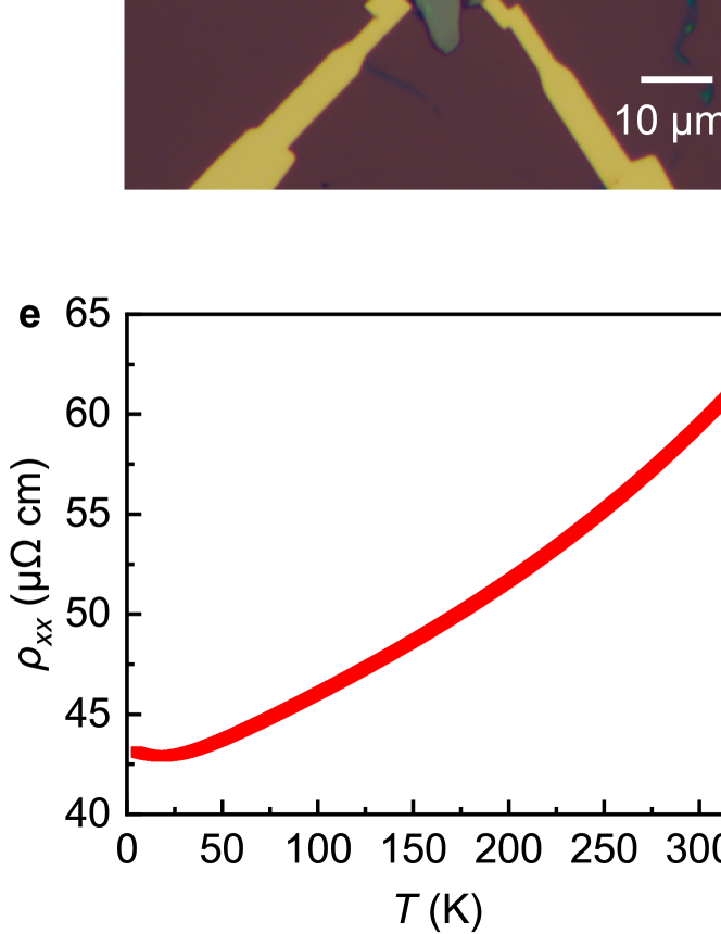
The Fe3GaTe2 thin flakes were exfoliated from high-quality bulk crystals grown by self-flux method. As is shown in Fig. 1a, Fe3GaTe2 has a layered structure with a hexagonal structure (space group )4, isostructural to Fe3GeTe2, and the fitted lattice parameters and from the single-crystal X-ray diffraction (XRD) pattern is 0.409(2) nm and 1.607(2) nm, respectively, which are consistent with previous results 4. In the Fe-Ga-Te layer, the Fe-Ga slab is sandwiched by the Te atoms and there is a vdW gap between two adjacent Fe-Ga-Te slabs, thus it can be exfoliated easily. Fig. 1b shows the XRD pattern of a Fe3GaTe2 single crystal and only sharp (00) diffraction peaks are observable, indicating that the crystal surface is normal to the -axis with the plate-shaped surface parallel to the -plane. Fig. 1c displays a typical device with a Hall bar geometry. The device is made by attaching the Fe3GaTe2 thin flake on a pre-prepared Ti/Au electrode and covered by h-BN for protection from H2O and O2. The thickness of this simple determined by the atomic force microscopy (AFM) (Fig. 1d) is around 12 nm. As shown in Fig. 1e, Fe3GaTe2 with = 12 nm shows a metallic behavior in the range of 18 K - 320 K, and there is Kondo-like minimum at 18 K, similar to the results of Fe3GaTe2 thin flakes in the literature4. Fig. 1f exhibits the field dependence of Hall resistivity at 300 K with current = +0.01 mA and -0.01 mA applied along the -plane. The obvious hysteresis loop in the curves clearly indicates that the room-temperature -axial hard ferromagnetism persists in the Fe3GaTe2 thin flake. Moreover, it can be seen that with small (= 0.01 mA) ,the curves with opposite current directions are almost same shape and both of them have identical ( 70 Oe).
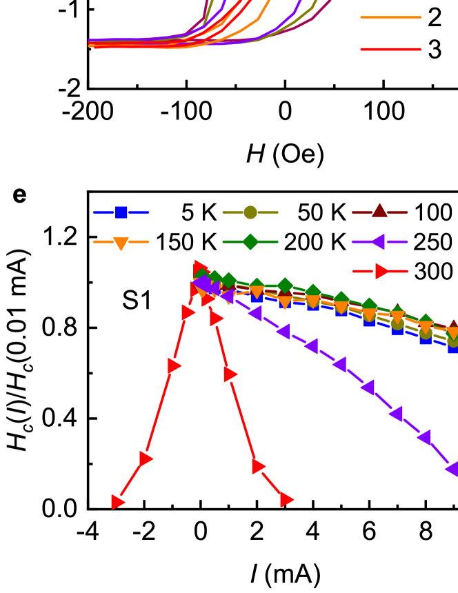
Fe3GaTe2 thin flakes exhibit an obvious behavior of current-dependent . Taking the device with = 12 nm (sample 1, S1) as an example (Fig. 2a), at = 5 K, the hysteresis loop becomes smaller with the decreased when the increases. The is around 2.5 kOe under = 0.01 mA and decrease to 1.8 kOe when a the 9 mA current is applied (Fig. 2b). In contrast to the significant changes of , the saturation Hall resistivity related to the saturation magnetization is almost intact. Importantly, as shown in Figs. 2c and 2d, the current-controlled still exists at room temperature ( = 300 K). For = 0.01 mA, the is 70 Oe and with increasing current the decreases gradually. Finally it becomes almost zero at = 3 mA. On the other hand, the is barely changed with current, similar to the results at 5 K. It implies that the ferromagnetic order is not been affected by the in-plane current and thus Fe3GaTe2 is suitable for spintronics at room temperature. Fig. 2e displays the evolution of reduced vs. at different temperatures. The curves at the low-temperature region (= 5 - 200 K) exhibit similar behavior while the decreases with increasing current more quickly at 250 K and 300 K. The larger current tunability of at both temperatures can be partially ascribed to the weakened ferromagnetism because of the stronger thermal fluctuations at higher temperature. To confirm the reproducibility of properties of our devices, we measured several samples with different thicknesses (S1 - S3). They exhibit a similar reduction of via and the of thinner sample decreases with more quickly (Fig. S1 in Supporting Information). Fig. 2f shows the relationship between reduced and current density at 300 K. It can be seen that all of curves for three devices almost fall on the same line, and the current reduces by 50 % for 5 mA/m2 when the disappears at around = 12.5 mA/m2.
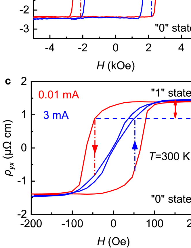
Based on the current-controlled coercivity reduction, we demonstrate that a highly energy-efficient nonvolatile spin memory device can be realized in Fe3GaTe2 thin flakes at room temperature, in which magnetic information is written by and read through the . Fig. 3a shows the hysteresis loop of under 0.01 mA and 9 mA at 5 K. The negative and positive saturated magnetization states are defined as “0” and “1" states. When sweeping the field from -5 kOe to 2.2 kOe, the initial state of device is on the “0" state. Then a large writing current of 9 mA is applied and because the is significantly reduced by , the magnetization of the Fe3GaTe2 device can be switched by current from “0" state to “1" state (blue arrow). Correspondingly, the “1” state at -2.2 kOe initially can also be altered to “0" state by the large (9 mA) (red arrow). Fig. 3b shows the detailed switching process of states through the - (-5 kOe) as a function of path (0 9 -9 9 mA) under various fields from -5 kOe to 5 kOe. For the “0" state at = -5 kOe and the “1" state at = 5 kOe in Fe3GaTe2 device, they are stable regardless of current sweep (purple and green curves). When fixing the field at 2.2 kOe, the increase of from 0 to 9 mA leads to the change of magnetization gradually from - (“0" state) to + (“1" state). Importantly, after reaching the “1" state, the magnetization is unchanged even the sweeps back to - 9 mA and forth 9 mA again. It is clearly indicate that the magnetic information switching from “0" to “1" states through is robust and nonvolatile (blue curve). Similarly, the reverse switching from “1" to “0" states can also be realized using the same path with the field at -2.2 kOe (red curve). On the other hand, the magnetic information (the value of ) can be read using a small current without disturbing the magnetization status. Similar results are also observed when = 1.8 kOe and 2.0 kOe (Fig. S2 in Supporting Information), indicating that there is a relatively wide window of magnetic field to switch the “0" and “1" states by current. More importantly, such switching of magnetic states driven by current persists up to room temperature ( = 300 K) (Figs. 3c and 3d). As shown in Fig. 3d, the “0" state at = -1 kOe and the “1" state at = 1 kOe are robust to the switching process (0 3 -3 3 mA) (purple and green curves). When fixing the field at 20 Oe, the increase of from 0 to 3 mA can switch the magnetization gradually, similar to the case at 5 K. In addition, the minimum ( 1 mA) changing the “0" and “1" states at 300 K is much smaller than that at 5 K ( 6 mA). Meanwhile, the field where the current can switch magnetic states also becomes very low (below 100 Oe). These behaviors are consistent with the significant reduction of with at 300 K (Fig. 2e). It is noted that at 300 K the hysteresis loop of curve at 0.01 mA is not a rectangular shape and it disappears at 3 mA, thus the initial and final states at 20 Oe is slightly different from the “0" and “1" states at 1 kOe (green arrows in Figs. 3c and 3d). But the switching between the initial and final states at 20 Oe is still large enough to be discerned.
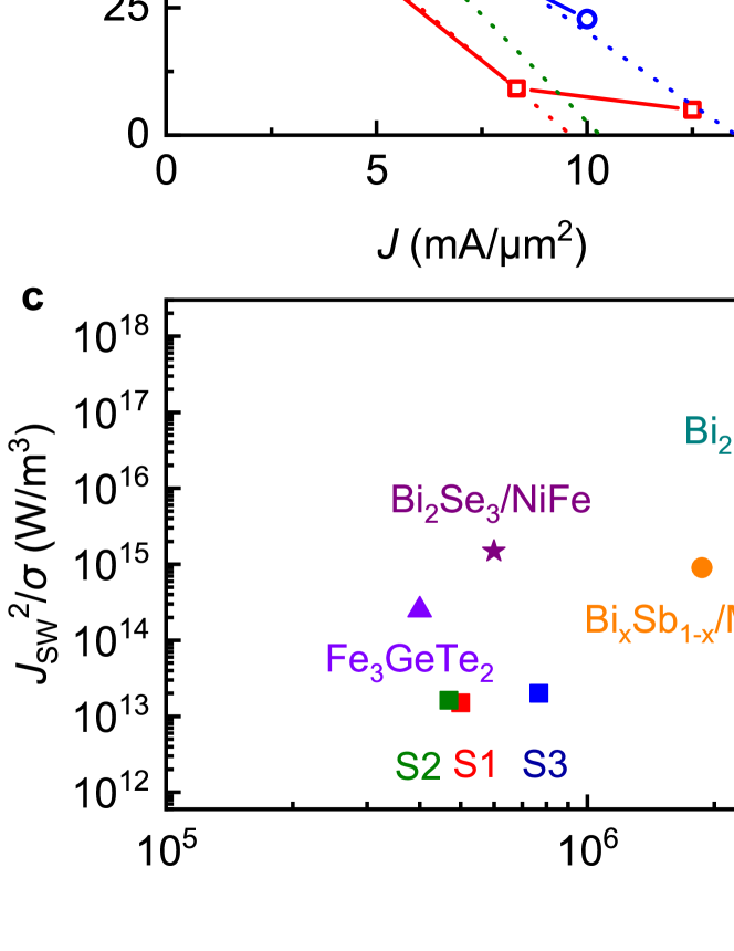
Next, we try to explain the electrical modulation of qualitatively based on the SOT effect generated by an in-plane current in Fe3GaTe2 itself due to its special geometrical structure same as Fe3GeTe24. Previous studies on Fe3GeTe2 indicate that an in-plane current density J = (, , 0) can induce a SOT = - acting on M = (, , ), where is the gyromagnetic ratio and the is the effective SOT magnetic field17, 23. And the symmetry of the crystal determines the dependence of on m and J and it can be expressed as = [( - - ( + ], where m = (, , ) = M/ is the magnetization unit vector and is the strength of the magnetoelectric coupling, determined by the spin-orbital coupling17, 23. Moreover, the can be obtained from an effective free energy density by = -/ with = . Combined with the magnetocrystalline anisotropy energy (MAE) for Ising-type out-of-plane easy-axis ferromagnet = -, we have the zero-field effective free energy density = + . If considering a spatially uniform magnetization and use a spherical basis, (, , ) = (sincos, sinsin, cos) and (, , ) = (cos, sin, 0), it has = -[cos2 + sin2cos(2 + )] 17, 23. For = 0, the has a minimum value of -/2 at m = and a maximum value of 0 when m lies in the plane. Therefore, the free energy barrier for switching the magnetization from m = - to m = + is /2. In contrast, the existence of in-plane modifies this free energy barrier to ( - )/2, i.e., the effectively reduce the barrier height between the local minima of the free energy 17. Correspondingly, the coercive field is also reduced from at = 0 to - at finite in-plane in a single domain case. This linear behavior is clearly observed from the curves for S1 - S3 of Fe3GaTe2 at 300 K (Fig. 4a). The linear fits of curves at the low current density range give = 7.0(3), 5.7(3), and 8.4(5) Oe/(mA/m2), respectively. These values are comparable with Fe3GeTe2/Pt bilayer system24, and one order of magnitude larger than those in the conventional heavy metal multiplayer films, such as Pt/Co and Pt/Fe etc 17, 24, 25, 26, 27, 28 (Fig. 4(b)). Moreover, although the of Fe3GaTe2 in present work is somewhat smaller than that of Fe3GeTe2 device 17, the work temperature of Fe3GaTe2 device at 300 K make it significantly superior to Fe3GeTe2. On the other hand, lowering switching current density and power dissipation ( = 1/ is conductivity) are important to improve the energy efficiency of memory device. These two parameters of three Fe3GaTe2 device have been calculated and shown in Fig. 4c. At 300 K, the and are in the range of 4.7(1)-7.7(3)105 A/cm2 and 1.5(0)-2.0(0)1013 W/m3, both of which are significantly smaller than most of composite SOT systems. For example, the and of Fe3GaTe2 are about 300 and 60000 times smaller than conventional heavy-metal/magnet SOT Pt/Co system27. In addition, when compared with Fe3GeTe2, both of them have similarly small but the of Fe3GaTe2 is one order of magnitude lower than that of Fe3GeTe2, highlighting the high energy efficiency of present Fe3GaTe2 devices.
In summary, the electrical control of coercive field in Fe3GaTe2 thin flake devices is observed up to room temperature. In addition, the room-temperature nonvolatile magnetization switching behavior at very low field ( 20 Oe) with a small in-plane current density ( 5.0105 A/cm2) and the remarkably low power dissipation ( 1.50 1013 W m-3) is realized. These behaviors can be partially ascribed to the unique SOT effect in Fe3GaTe2. Such capability of high-efficiency nonvolatile magnetization switching by current at room temperature make Fe3GaTe2 become a very promising system for spintronic applications using 2D magnetic vdW materials.
2.1 Methods
Single crystal growth and structural characterization. Single crystals of Fe3GaTe2 were grown by self-flux method. Flakes of Fe (99.98 % purity), Ga (99.99 % purity) and Te (99.99 %) in a molar ratio of 1 : 1 : 2 were put into a quartz tube. The tube was evacuated and sealed at 0.01 Pa. The sealed quartz ampoule was heated to 1273 K for 10 hours and are then held there for another one day, then held there for another one day, then the temperature was quickly decrease down to 1153 K witnin 2 h followed by slowly cooled down to 1053 K within 100 h. Finally, the ampoule was taken out from the furnace and decanted with a centrifuge to separate Fe3GaTe2 single crystals from the flux. In order to avoid degradation, the Fe3GaTe2 single crystals are stored in an Ar-filled glovebox. The XRD pattern of a Fe3GaTe2 single crystal was measured using a Bruker D8 Advance X-ray machine with Cu K ( = 1.5418 Å) radiation. For the fit of lattice parameters of Fe3GaTe2, the single-crystal XRD pattern was measured using a Bruker D8 Quest X-ray machine with Mo K ( = 0.7107 Å) radiation. The microscopy images was acquired using a Bruker Edge Dimension atomic force microscope (AFM).
Device fabrication. Fe3GaTe2 flakes were cleaved from bulk crystals onto polydimethylsiloxane (PDMS) by mechanical exfoliation and they were examined by an optical microscope to evaluate the thickness roughly. Then the atomically smooth flakes with desired thicknesses were transferred to a 285 nm SiO2/Si substrate with pre-patterned electrodes and an -BN capping layer was used to cover the sample for protection from H2O and O2. The Ti/Au (10/40 nm) electrodes was fabricated by electron beam lithography and metals were deposited using thermally evaporating method. After transport measurements, the -BN capping layer was removed and the thickness of sample was determined precisely by AFM. The whole fabrication process of device was carried out in an argon glove box with H2O and O2 contents less than 0.1 ppm to avoid degradation of the samples.
Electrical transport measurements. Magnetization and electrical transport measurements were performed in a Quantum Design MPMS3 and superconducting magnet system (Cryomagnetics, C-Mag Vari-9). Both longitudinal and Hall electrical resistance were measured using a five-probe method on Fe3GaTe2 Hall bar device with current flowing in the plane. In dc measurements, the bias current was generated by using a current source (Keithley, 6221) and the voltage was measured with a nanovoltmeter (Keithley, 2182A). The raw Hall resistance was measured by sweeping the field up to 5 kOe at various temperatures, and the Hall resistance was determined by a standard symmetrization procedure to remove the contribution of magnetoresistance from the raw Hall data due to voltage probe misalignment30.
Figure S1. The as a function of current for three devices at 300 K; Figure S2. Nonvolatile magnetization switching by current under fields 1.8 kOe and 2.0 kOe at 5 K.
This work was supported by National Key R&D Program of China (Grants Nos. 2018YFE0202600 and 2022YFA1403800), Beijing Natural Science This work was supported by National Key R&D Program of China (Grants Nos. 2018YFE0202600 and 2022YFA1403800), Beijing Natural Science Foundation (Grant No. Z200005), National Natural Science Foundation of China (Grants No. 12174443), the Fundamental Research Funds for the Central Universities and Research Funds of Renmin University of China (RUC) (Grants Nos. 18XNLG14 and 19XNLG17), the Outstanding Innovative Talents Cultivation Funded Programs 2022 of Renmin University of China, Beijing National Laboratory for Condensed Matter Physics, and Collaborative Research Project of Laboratory for Materials and Structures, Institute of Innovative Research, Tokyo Institute of Technology.
References
- 1 Gong, C.; Li, L.; Li, Z.; Ji, H.; Stern,A.; Xia, Y.; Cao, T.; Bao, W.; Wang, C.; Wang, Y.; Qiu, Z. Q.; Cava, R. J.; Louie, S. G.; Xia, J.; Zhang, X. Discovery of intrinsic ferromagnetism in two-dimensional van der Waals crystals. Nature 2017, 546, 265-269.
- 2 Huang, B.; Clark, G.; Navarro-Moratalla, E.; Klein, D. R.; Cheng, R.; Seyler, K. L.; Zhong, D.; Schmidgall, E.; McGuire, M. A.; Cobden, D. H.; Yao, W.; Xiao, D.; Jarillo-Herrero, P.; Xu, X. Layer-dependent ferromagnetism in a van der Waals crystal down to the monolayer limit. Nature 2017, 546, 270-273.
- 3 Deng, Y.; Yu, Y.; Song, Y.; Zhang, J.; Wang, N. Z.; Sun, Z.; Yi, Y.; Wu, Y. Z.; Wu, S.; Zhu, J.; Wang, J.; Chen, X. H.; Zhang, Y. Gate-tunable room-temperature ferromagnetism in two-dimensional Fe3GeTe2. Nature 2018, 563, 94-99.
- 4 Zhang, G.; Guo, F.; Wu, H.; Wen, X.; Yang, L.; Jin, W.; Zhang, W.; Chang, H. Above-room-temperature strong intrinsic ferromagnetism in 2D van der Waals Fe3GaTe2 with large perpendicular magnetic anisotropy. Nat. Commun. 2022, 13, 5067.
- 5 Tian, S.; Zhang, J.-F.; Li, C.; Ying, T.; Li, S.; Zhang, X.; Liu, K.; Lei, H. Ferromagnetic van der Waals Crystal VI3. J. Am. Chem. Soc. 2019, 141, 5326-5333.
- 6 Lee, J.-U.; Lee, S.; Ryoo, J. H.; Kang, S.; Kim, T. Y.; Kim, P.; Park, C.-H.; Park, J.-G.; Cheong, H. Ising-Type Magnetic Ordering in Atomically Thin FePS3.Nano Lett. 2016, 16, 7433-7438.
- 7 Lee, K.; Dismukes, A. H.; Telford, E. J.; Wiscons, R. A.; Wang, J.; Xu, X.; Nuckolls, C.; Dean, C. R.; Roy, X.; Zhu, X. Magnetic Order and Symmetry in the 2D Semiconductor CrSBr Nano Lett. 2021, 21, 3511-3517.
- 8 Geim, A. K.; Grigorieva, I. V. Van der Waals heterostructures. Nature 2013, 499, 419-425.
- 9 Novoselov, K. S.; Mishchenko, A.; Carvalho, A.; CastroNeto, A. H. 2D materialsand van der Waals heterostructures. Science 2016, 353, aac9439.
- 10 Liu, Y.; Weiss, N. O.; Duan, X.; Cheng, H.-C.; Huang, Y.; Duan, X. Van der Waals heterostructures and devices. Nat. Rev. Mater. 2016, 1, 16042.
- 11 Deiseroth, H.-J.; Aleksandrov, K.; Reiner, C.; Kienle, L.; Kremer, R. K. Fe3GeTe2 and Ni3GeTe2 - Two new layered transition-metal compounds: Crystal structures, HRTEM investigations, and magnetic and electrical properties. Eur. J. Inorg. Chem. 2006, 8, 1561.
- 12 May, A. F.; Ovchinnikov, D.; Zheng, Q.; Hermann, R.; Calder, S.; Huang, B.; Fei, Z.; Liu, Y.; Xu, X.; McGuire, M. A. Ferromagnetism Near Room Temperature in the Cleavable van der Waals Crystal Fe5GeTe2. ACS Nano 2019, 13, 4436-4442.
- 13 Seo, J.; Kim, D. Y.; An, E. S.; Kim, K.; Kim, G.-Y.; Hwang, S.-Y.; Kim, D. W.; Jang, B. G.; Kim, H.; Eom, G.; et al. Nearly room temperature ferromagnetism in a magnetic metal-rich van der Waals metal. Sci. Adv. 2020, 6, eaay8912.
- 14 Li, Z,; Tang, M.; Huang, J.; Qin, F.; Ao, L.; Shen, Z.; Zhang, C.; Chen, P.; Bi, X.; Qiu, C.; Yu, Z.; Zhai, K.; Ideue, T.; Wang, L.; Liu, Z.; Tian, Y.; Iwasa, Y.; Yuan, H. Magnetic Anisotropy Control with Curie Temperature above 400 K in a van der Waals Ferromagnet for Spintronic Device. Adv. Mater. 2022, 34, 2201209.
- 15 Eyers, E. B.; Ralph, D. C.; Katine, J. A.; Louie, R. N.; Buhrman, R. A. Current-induced switching of domains in magnetic multilayer devices. Science 1999, 285, 867.
- 16 Wang, Q. Y.; Zeng, Y.; Yuan, K.; Zeng, Q. Q.; Gu, P. F.; Xu, X. L.; Wang, H. W.; Han, Z.; Nomura, K.; Wang, W. H.; Liu, E. K.; Hou, Y. L.; Ye,Y. Magnetism modulation in Co3Sn2S2 by current-assisted domain wall motion. Nat. Electron. 2022, 6, 119.
- 17 Zhang, K.; Han, S.; Lee, Y.; Coak, M. J.; Kim, J.; Hwang, I.; Son, S.; Shin, J.; Lim, M.; Jo, D.; Kim, K.; Kim, D.; Lee, H.-W.; Park, J.-G. Gigantic Current Control of Coercive Field and Magnetic Memory Based on Nanometer-Thin Ferromagnetic van der Waals Fe3GeTe2. Adv. Mater. 2021, 33, 2004110.
- 18 Zhang, K.; Lee, Y.; Coak, M. J.; Kim, J.; Son, S.; Hwang,I.; Ko, D.-S.; Oh, Y.; Jeon, I.; Kim, D.; Zeng, C.; Lee, H.-W.; Park, J.-G. Highly Efficient Nonvolatile Magnetization Switching and Multi-Level States by Current in Single Van der Waals Topological Ferromagnet Fe3GeTe2. Adv. Funct. Mater. 2021, 31, 2105992.
- 19 Zhu, W. K.; Xie, S. H.; Lin, H. L.; Zhang, G. J.; Wu, H.; Hu, T. G.; Wang, Z.; Zhang, X. M.; Xu, J. H.; Wang, Y. J.; Zheng, Y. H.; Yan, F. G.; Zhang, J.; Zhao, L. X.; Patane, A.; Zhang, J.; Chang, H. X.; Wang, K. Y. Large room-temperature magnetoresistance in van der Waals ferromagnet/semiconductor junctions. Chin. Phys. Lett. 2022, 39, 128501.
- 20 Yin, H.; Zhang, P.; Jin, W.; Di, B.; Wu, H.; Zhang, G.; Zhang, W.; Chang, H. Fe3GaTe2/MoSe2 Ferromagnet/Semiconductor 2D van der Waals Heterojunction for Room-Temperature Spin-Valve Devices. CrystEngComm, 2023, 25, 1339-1346.
- 21 Jin, W.; Zhang, G.; Wu, H.; Yang, L.; Zhang, W.; Chang, H. Room-Temperature Spin-Valve Devices Based on Fe3GaTe2/MoSe2/Fe3GaTe2 2D van der Waals Heterojunctions. Nanoscale, 2023, 15, 5371-5378.
- 22 Li, W.; Zhu, W.; Zhang, G.; Wu, H.; Zhu, S.; Li, R.; Zhang, E.; Zhang, X.; Deng, Y.; Zhang, J.; Zhao, L.; Chang, H.; Wang, K. Room-temperature van der Waals 2D ferromagnet switching by spin-orbit torques. 2023, arXiv: 2304.10718
- 23 Johansen, O.; Risinggard, V.; Sudbo, A.; Linder, J.; Brataas, A. Current Control of Magnetismin Two-Dimensional Fe3GeTe2. Phys. Rev. Lett. 2019, 122, 217203.
- 24 Wang, X.; Tang, J.; Xia, X.; He, C.; Zhang, J.; Liu, Y.; Wan, C.; Fang, C.; Guo, C.; Yang, W.; et al. Current-driven magnetization switching in a van der Waals ferromagnet Fe3GeTe2. Sci. Adv. 2019, 5, eaaw8904.
- 25 Khang, N. H. D.; Ueda, Y.; Hai, P. N. A conductive topological insulator with large spin Hall effect for ultra low power spin-orbit torque switching. Nat. Mater. 2018, 17, 808-813.
- 26 Han, J.; Richardella, A.; Siddiqui, S. A.; Finley, J.; Samarth, N.; Liu, L. Room-Temperature Spin-Orbit Torque Switching Induced by a Topological Insulator. Phys. Rev. Lett. 2017, 119, 077702.
- 27 Garello, K.; Miron, I. M.; Avci, C. O.; Freimuth, F.; Mokrousov, Y.; Blugel, S.; Auffret, S.; Boulle, O.; Gaudin, G.; Gambardella, P. Symmetry and magnitude of spin-orbit torques in ferromagnetic heterostructures. Nat. Nanotechnol. 2013, 8, 587.
- 28 DC, M.; Grassi, R.; Chen, J.-Y.; Jamali, M.; Hickey, D. R.; Zhang, D.; Zhao, Z.; Li, H.; Quarterman, P.; Lv, Y.; Li, M.; Manchon, A.; Mkhoyan, K. A.; Low, T.; Wang, J.-P. Room-temperature high spin-orbit torque due to quantum confinement in sputtered BixSe(1-x) films. Nat. Mater. 2018, 17, 800-807.
- 29 Wang, Y.; Zhu, D.; Wu, Y.; Yang, Y.; Yu, J.; Ramaswamy, R.; Mishra, R.; Shi, S.; Elyasi, M.; Teo, K.-L.; Wu, Y.; Yang, H. Room temperature magnetization switching in topological insulator-ferromagnet heterostructures by spin-orbit torques. Nat. Commun. 2017, 8, 1364.
- 30 Ohno, H.; Munekata, H.; Penny, T.; Molnar, S. V.; Chang, L. L. Magnetotransport properties of p-type (In,Mn)As diluted magnetic III-V semiconductors. Phys. Rev. Lett. 1992, 68, 2664.