Non-Hermitian topological ohmmeter
Abstract
Measuring large electrical resistances forms an essential part of common applications such as insulation testing, but suffers from a fundamental problem: the larger the resistance, the less sensitive a canonical ohmmeter is. Here we develop a conceptually different electronic sensor by exploiting the topological properties of non-Hermitian matrices, whose eigenvalues can show an exponential sensitivity to perturbations. The ohmmeter is realized in an multi-terminal, linear electric circuit with a non-Hermitian conductance matrix, where the target resistance plays the role of the perturbation. We inject multiple currents and measure a single voltage in order to directly obtain the value of the resistance. The relative accuracy of the device increases exponentially with the number of terminals, and for large resistances outperforms a standard measurement by over an order of magnitude. Our work paves the way towards leveraging non-Hermitian conductance matrices in high-precision sensing.
Small changes typically produce small effects. This common physical intuition has its roots in mathematics, where according to Weyl’s inequality, the spectrum of a Hermitian matrix cannot change by an amount larger than the perturbation. Non-Hermitian matrices, however, are not constrained in this fashion. Instead, a small change can produce a large shift of the spectrum, in some cases even growing exponentially as a function of the matrix dimension. This counter-intuitive property has recently been proposed as a way of constructing new sensor architectures [1, 2, 3, 4]: In certain condensed-matter and optical systems, gain and loss may lead to an effectively non-Hermitian description of wavefunction dynamics exhibiting enhanced sensitivity to small parameter changes. Specifically, an exponentially enhanced spectral sensitivity with respect to boundary conditions has been predicted [4] to occur as a consequence of nontrivial topology: it is protected by an integer-quantized winding number of the complex spectrum [5, 6, 7, 8].
In parallel, it was realized that signatures of nontrivial topology are not unique to condensed-matter systems, but can occur in a variety of other platforms, dubbed metamaterials [9, 10, 11, 12, 13, 14]. Their dynamics mimics that of quantum wavefunctions evolving according to the Schrödinger equation, allowing for the experimental demonstration of different non-Hermitian topological phenomena [15, 16, 17, 18, 19, 20, 21, 22, 23, 24, 25].
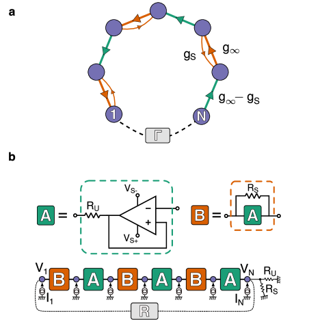
Here, starting from these insights and with a focus on applications, we build a classical electronic circuit with a non-Hermitian topological conductance matrix [26, 27] that functions as an ohmmeter. We consider a multiterminal system connected to a set of current sources and voltmeters that, in linear order, is described by a conductance matrix relating the current vector ) to the voltage vector ). We used resistors and operational amplifiers connected in voltage followers configuration to build a circuit associated to a non-Hermitian conductance matrix as shown in Fig. 1. The sensor circuit realizes an electronic counterpart of a non-Hermitian topological system investigated theoretically in the context of tight-binding models in Ref. [4] (details in Methods Sec. M1). Here, the role of the Hermitian coupling term between the first and the last sites of the tight-binding Hamiltonian is played by the resistor in Fig. 1b. In this work, we make use of the topological properties of the non-Hermitian -matrix to measure the very large resistance of the device under test (DUT) with enhanced precision.
A standard method to measure large resistances is the constant voltage method where a known (large) voltage is sourced and the current flowing through the DUT is measured. The resistance is given by the ratio between the voltage applied on the DUT and the current, the latter being usually determined by measuring the voltage drop on a well-calibrated test resistance. Such a current vanishes as the resistance of the DUT increases and high precision measurements of infinitesimal currents are required to achieve a decent measurement of resistances above the regime. The precision of the current measurement sets the precision of the resistance measurement, which decreases continuously when increases. Unlike the standard method, we consider here a multiple-source device whose sensitivity increases exponentially with the number of terminals.
The conductance matrix of the electronic circuit in Fig. 1 (for five terminals) is of the form
| (1) |
where , and . is the unidirectional resistance associated to the voltage follower, is a resistance that appears between adjacent terminals in a staggered way, and is the resistance of the DUT, that connects the first terminal to the last one in our electronic circuit, controlling the boundary condition. Since we are interested in measuring small variations in the large , we consider the regime where so that the resistance is only perturbatively connecting the first terminal to the last one. The difference between Eq. (1) and the tight-binding Hamiltonian matrix considered in Ref. [4] is the at the two ends of the main diagonal (for more information on the non-Hermitian tight-binding model, see Methods Sec. M1).
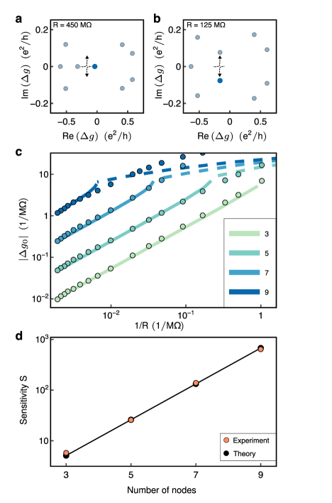
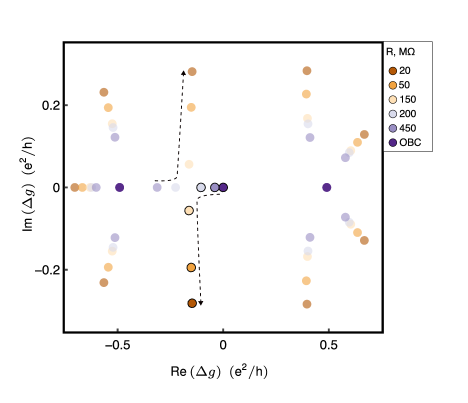
We consider the right eigenvalue problem, where are the right voltage eigenvectors of the conductance matrix and is the corresponding eigenvalue (for non-Hermitian matrices left and right eigenvectors are not equivalent, for mathematical details see, e.g. Ref. [28]). Taking the () limit, we get the open boundary condition of the non-Hermitian matrix. In this case, for any odd number of terminals, the matrix is guaranteed to have an eigenvalue equal to . In the language of condensed-matter physics this property is a consequence of sublattice symmetry (see Methods Sec. M1). We focus on the eigenvalue below.
For finite resistance , the shift of is given by (see Fig. 2a, b and c). For large enough , the modulus of is well separated from the modulus of any other eigenvalue (see Fig. 2a). We call this the perturbative, or ‘separated eigenvalues’ regime. Going to smaller this no longer holds: as shown in Fig. 2a, b, merges with another eigenvalue as is decreased. The pair of eigenvalues then acquire nonzero imaginary parts and have equal absolute values. More details on the eigenvalues as a function of are shown in the Methods Sec. M2.
At large enough resistances, where the eigenvalue is well separated, we can use perturbation theory [4] to track the evolution of (for details see Methods Sec. M1):
| (2) |
Here, and are the left and right eigenvectors of at , and is the number of terminals. We also calculate the change as a function of numerically from as shown in Fig. 2c with the solid and dashed lines, the solid lines showing where the perturbative results are valid. The figure shows that for more terminals the resistances where the perturbative results hold get larger. We note that, in parallel to our work, such a shift of the eigenvalues was recently measured in optics [29] and it was used to measure capacitances in electronic circuits [30].
Using the definition of Ref [4] for the sensitivity as the change of the eigenvalue with respect to the change in boundary condition we get
| (3) |
The expected perturbative values for the sensitivity are shown in Fig. 2d. In practice, and may take a large range of values, and could be optimized such as to produce a maximal sensitivity to the target resistance . For a proof of principle we take here and – a precise optimization is beyond our present scope.
We connect the first and the last terminal with a resistance and inject the current eigenvector in the device (see Sec. M1 and Sec. M3). Note that this means multiple current sources are used simultaneously. Each of the currents is generated by applying a low frequency AC voltage on a resistor with the source of a lock-in amplifier. Lock-in amplifiers are also used to measure the voltages on the terminals (see Sec. M3). Measuring the voltage on the last terminal and dividing by the current on the last terminal enables us to experimentally determine the eigenvalue shift, since (see Sec. M1 for details)
| (4) |
The measured values for are shown in Fig. 2c together with the theoretical prediction. The value of is determined separately for each point by measuring without connecting the resistance prior to any finite measurement, in order to get rid of slow drifts of the voltages, and each data point corresponds to an averaging over 30 measurements (see Methods Sec. M3 for details). There is a very good agreement between the experimental data and the exact eigenvalues for large values, where the perturbative results hold.
Using the measured value for the voltage and the value for the injected current we can also estimate as:
| (5) |
We calculate the experimental value of using this formula for resistances in the range of validity of the perturbative theory (based on the solid lines of Fig. 2c). The results are shown on Fig. 2d and they are in good agreement with the theoretical predictions.
For small changes of the large target resistance the sensor gives an ohmic relationship between and the change in voltage : . We therefore define the dimensionless relative slope as
| (6) |
is independent of the input current and can be expressed as (see Methods Sec. M1 for details)
| (7) |
characterizes the relative accuracy of our device. The relative accuracy of the resistance measurement () depends on the relative accuracy of the voltage measurement () as
| (8) |
Larger thus improves the accuracy of the device. From Eq. (7) we can see that always holds and from Eq. (3) we can see that grows monotonically as a function of the number of terminals, . This means that for a given resistance the accuracy can be improved by increasing the number of nodes, provided that the perturbation theory results hold.
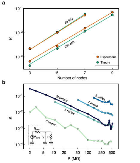
The theoretical values for and the experimentally obtained values are shown on Fig. 3a as a function of the number of terminals , for which the perturbative theory holds and for two different test resistances ( and ). The measurement procedure is described in details in the Methods Sec. M3.
In order to compare the performance of the non-Hermitian ohmmeter with a standard measurement, we measure the resistance with the circuit shown in the inset of Fig. 3b, corresponding to the simplest configuration of a standard single-terminal circuit. We use the same lock-in amplifiers for sourcing and measuring as for the non-Hermitian ohmmeter. In this circuit, the well-calibrated resistance allows us to determine the current flowing through the resistance of the DUT, , leading to the trivial voltage divider relation between the measured voltage and the resistance to be measured : . In the constant voltage mode, should be as large as possible to maximize the accuracy of the measurement but it should remain much smaller than the resistance in parallel with the input resistance of the lock-in amplifier ( 10M) to ensure a constant voltage drop on . We choose M, a value that fulfilled these two conditions and that corresponds to the polarisation resistance used for the non-Hermitian ohmmeter. The results are shown in Fig. 3b. The parameter shows the same trend as a function of for all measurements, but can be exponentially increased for a larger number of terminals of the non-Hermitian device. Thus, we observe that the accuracy of the non-Hermitian ohmmeter outperforms that of the simple, single-terminal measurement starting at , and becomes one order of magnitude larger at .
Author contributions
ICF and JCB conveived the theoretical framework of the project, ICF, JvdB, and JD supervised the project. KO, AC and JD designed the circuit, conducted the measurements and analysed the data. VK performed the analytic calculations and numerical simulations using the idealized and measured conductance matrices to test the feasibility of the device with inputs from JCB, JvdB, and ICF. All authors participated in interpreting the results and writing the manuscript.
Data availability
The data and codes used in this work are available on Zenodo at [31].
Acknowledgements
This work was supported by the Deutsche Forschungsgemeinschaft (DFG, German Research Foundation) under Germany’s Excellence Strategy through the Würzburg-Dresden Cluster of Excellence on Complexity and Topology in Quantum Matter – ct.qmat (EXC 2147, project-ids 390858490 and 392019).
References
- Wiersig [2014] J. Wiersig, Enhancing the sensitivity of frequency and energy splitting detection by using exceptional points: Application to microcavity sensors for single-particle detection, Phys. Rev. Lett. 112, 203901 (2014).
- Hodaei et al. [2017] H. Hodaei, A. U. Hassan, S. Wittek, H. Garcia-Gracia, R. El-Ganainy, D. N. Christodoulides, and M. Khajavikhan, Enhanced sensitivity at higher-order exceptional points, Nature 548, 187 (2017).
- Chen et al. [2017] W. Chen, Ş. K. Özdemir, G. Zhao, J. Wiersig, and L. Yang, Exceptional points enhance sensing in an optical microcavity, Nature 548, 192 (2017).
- Budich and Bergholtz [2020] J. C. Budich and E. J. Bergholtz, Non-hermitian topological sensors, Physical Review Letters 125, 10.1103/physrevlett.125.180403 (2020).
- Gong et al. [2018] Z. Gong, Y. Ashida, K. Kawabata, K. Takasan, S. Higashikawa, and M. Ueda, Topological phases of non-Hermitian systems, Phys. Rev. X 8, 031079 (2018).
- Borgnia et al. [2020] D. S. Borgnia, A. J. Kruchkov, and R. J. Slager, Non-Hermitian Boundary Modes and Topology, Phys. Rev. Lett. 124, 056802 (2020).
- Okuma et al. [2020] N. Okuma, K. Kawabata, K. Shiozaki, and M. Sato, Topological Origin of Non-Hermitian Skin Effects, Phys. Rev. Lett. 124, 086801 (2020).
- Bergholtz et al. [2021] E. J. Bergholtz, J. C. Budich, and F. K. Kunst, Exceptional topology of non-hermitian systems, Rev. Mod. Phys. 93, 015005 (2021).
- Lu et al. [2014] L. Lu, J. D. Joannopoulos, and M. Soljačić, Topological photonics, Nature Photonics 8, 821 (2014).
- Albert et al. [2015] V. V. Albert, L. I. Glazman, and L. Jiang, Topological properties of linear circuit lattices, Physical Review Letters 114, 10.1103/physrevlett.114.173902 (2015).
- Yang et al. [2015] Z. Yang, F. Gao, X. Shi, X. Lin, Z. Gao, Y. Chong, and B. Zhang, Topological acoustics, Physical Review Letters 114, 10.1103/physrevlett.114.114301 (2015).
- Süsstrunk and Huber [2015] R. Süsstrunk and S. D. Huber, Observation of phononic helical edge states in a mechanical topological insulator, Science 349, 47 (2015).
- Hu et al. [2015] W. Hu, J. C. Pillay, K. Wu, M. Pasek, P. P. Shum, and Y. Chong, Measurement of a topological edge invariant in a microwave network, Physical Review X 5, 10.1103/physrevx.5.011012 (2015).
- Goldman et al. [2016] N. Goldman, J. C. Budich, and P. Zoller, Topological quantum matter with ultracold gases in optical lattices, Nature Physics 12, 639 (2016).
- Brandenbourger et al. [2019] M. Brandenbourger, X. Locsin, E. Lerner, and C. Coulais, Non-reciprocal robotic metamaterials, Nat. Commun. 10, 1 (2019).
- Lee and Thomale [2019] C. H. Lee and R. Thomale, Anatomy of skin modes and topology in non-hermitian systems, Physical Review B 99, 10.1103/physrevb.99.201103 (2019).
- Ghatak et al. [2020] A. Ghatak, M. Brandenbourger, J. Van Wezel, and C. Coulais, Observation of non-Hermitian topology and its bulk-edge correspondence in an active mechanical metamaterial, PNAS 117, 29561 (2020).
- Weidemann et al. [2020] S. Weidemann, M. Kremer, T. Helbig, T. Hofmann, A. Stegmaier, M. Greiter, R. Thomale, and A. Szameit, Topological funneling of light, Science 368, 311 (2020).
- Helbig et al. [2020] T. Helbig, T. Hofmann, S. Imhof, M. Abdelghany, T. Kiessling, L. W. Molenkamp, C. H. Lee, A. Szameit, M. Greiter, and R. Thomale, Generalized bulk–boundary correspondence in non-Hermitian topolectrical circuits, Nat. Phys. 16, 747 (2020).
- Xiao et al. [2020] L. Xiao, T. Deng, K. Wang, G. Zhu, Z. Wang, W. Yi, and P. Xue, Non-Hermitian bulk–boundary correspondence in quantum dynamics, Nat. Phys. 16, 761 (2020).
- Zhang et al. [2021a] X. Zhang, Y. Tian, J. H. Jiang, M. H. Lu, and Y. F. Chen, Observation of higher-order non-Hermitian skin effect, Nat. Commun. 12, 1 (2021a).
- Zhang et al. [2021b] L. Zhang, Y. Yang, Y. Ge, Y. J. Guan, Q. Chen, Q. Yan, F. Chen, R. Xi, Y. Li, D. Jia, S. Q. Yuan, H. X. Sun, H. Chen, and B. Zhang, Acoustic non-Hermitian skin effect from twisted winding topology, Nat. Commun. 12, 1 (2021b).
- Wang et al. [2021] H. Wang, X. Zhang, J. Hua, D. Lei, M. Lu, and Y. Chen, Topological physics of non-Hermitian optics and photonics: a review, J. Opt. 23, 123001 (2021).
- Liu et al. [2021] S. Liu, R. Shao, S. Ma, L. Zhang, O. You, H. Wu, Y. J. Xiang, T. J. Cui, and S. Zhang, Non-Hermitian Skin Effect in a Non-Hermitian Electrical Circuit, Research 2021, 1 (2021).
- Liang et al. [2022] Q. Liang, D. Xie, Z. Dong, H. Li, H. Li, B. Gadway, W. Yi, and B. Yan, Dynamic signatures of non-hermitian skin effect and topology in ultracold atoms, Physical Review Letters 129, 10.1103/physrevlett.129.070401 (2022).
- Franca et al. [2022] S. Franca, V. Könye, F. Hassler, J. van den Brink, and C. Fulga, Non-Hermitian physics without gain or loss: The skin effect of reflected waves, Phys. Rev. Lett. 129, 086601 (2022).
- Ochkan et al. [2023] K. Ochkan, R. Chaturvedi, V. Könye, L. Veyrat, R. Giraud, D. Mailly, A. Cavanna, U. Gennser, E. M. Hankiewicz, B. Büchner, J. van den Brink, J. Dufouleur, and I. C. Fulga, Observation of non-hermitian topology in a multi-terminal quantum hall device (2023), arXiv:2305.18674 [cond-mat.mes-hall] .
- Ashida et al. [2020] Y. Ashida, Z. Gong, and M. Ueda, Non-Hermitian physics, Adv. Phys. 69, 249 (2020).
- Parto et al. [2023] M. Parto, C. Leefmans, J. Williams, and A. Marandi, Enhanced sensitivity via non-hermitian topology (2023), arXiv:2305.03282 [physics.optics] .
- Yuan et al. [2023] H. Yuan, W. Zhang, Z. Zhou, W. Wang, N. Pan, Y. Feng, H. Sun, and X. Zhang, Non-hermitian topolectrical circuit sensor with high sensitivity, Advanced Science 10.1002/advs.202301128 (2023).
- Könye et al. [2023] V. Könye, K. Ochkan, A. Chyzhykova, J. C. Budich, J. van den Brink, I. C. Fulga, and J. Dufouleur, Non-hermitian topological ohmmeter, Zenodo 10.5281/zenodo.8268147 (2023).
- Su et al. [1979] W. P. W. Su, J. R. Schrieffer, and A. J. Heeger, Solitons in polyacetylene, Phys. Rev. Lett. 42, 1698 (1979).
- Lieu [2018] S. Lieu, Topological phases in the non-hermitian su-schrieffer-heeger model, Physical Review B 97, 10.1103/physrevb.97.045106 (2018).
- Hatano and Nelson [1996] N. Hatano and D. R. Nelson, Localization transitions in non-Hermitian quantum mechanics, Phys. Rev. Lett. 77, 570 (1996).
- Kunst et al. [2017] F. K. Kunst, M. Trescher, and E. J. Bergholtz, Anatomy of topological surface states: Exact solutions from destructive interference on frustrated lattices, Phys. Rev. B 96, 085443 (2017).
- Kunst et al. [2018] F. K. Kunst, E. Edvardsson, J. C. Budich, and E. J. Bergholtz, Biorthogonal bulk-boundary correspondence in non-hermitian systems, Phys. Rev. Lett. 121, 026808 (2018).
Methods
M1 non-Hermitian SSH model and perturbation theory results
The Eq (1) conductance matrix is equivalent to the Hamiltonian matrix of a non-Hermitian Su-Schrieffer-Heeger (SSH) model [32, 33]. The only difference is the present on the diagonal. The model has non-reciprocal staggered hoppings and plays the role of the onsite potential. Hoppings to the right are and , hoppings to the left are and , and is the hopping parameter between the first and last site. Ignoring the diagonal and setting the matrix has sublattice symmetry with . By choosing the length of the chain to be odd, this symmetry ensures that there is always a zero mode. Thus, with constant diagonal term and in the limit, the matrix will always have an eigenvalue .
Two different limits exist depending on the values of and . When the staggering dominates and the system is in a Su–Schrieffer–Heeger model [32] like phase. When the unidirectionality dominates and the system is in a Hatano-Nelson model [34] like phase. In our device, we choose a region in between these two limiting cases, closer to the Hatano-Nelson phase.
Now we show the derivation of the perturbative expressions presented in the main text. We take the Eq. (1) matrix with . The right and left eigenvectors corresponding to the eigenvalue can be calculated exactly as [35, 36].
| (M1) | ||||
| (M2) |
where and are normalizations in the units of voltage.
Using these eigenvectors the perturbative eigenvalue can be calculated as per Eq. (2).
Injecting the right eigenvectors as currents of the form (we use the normalization where the largest current is )
| (M3) |
the voltage on the last terminal can be expressed as [4]
| (M4) |
where . For three terminals this is
| (M5) |
The reflection matrix has an eigenvalue obeying , which can be expressed perturbatively as
| (M6) |
and since only the last element of is non-zero, the voltage on the last terminal can be expressed as
| (M7) |
where
| (M8) |
Using this formula for the voltage we can obtain Eqs. (4), (5) and (7) of the main text.
M2 Conductance matrix eigenspectra
Figure Fig. M1 shows the spectrum of the conductance matrix for additional values of (compare with Fig. 2a and Fig. 2b). The perturbation theory results hold while the eigenvalue is far away from the next eigenvalue, which we label . For 9 terminals this is true for resistances .
M3 Measurement details and procedure
We use AD 823A FET input operational amplifiers for building the electronic circuit. The voltages are measured with SR 830 lock-in amplifiers, with an input impedance of about 10 M. Measurements are done at low frequency ( Hz). In the case of 3, 5, 7, and 9 terminals, the current vectors used in the experiment [see Eq. (M3)] are given by
Figure M2 shows the voltage data used to calculate the values of K for various system sizes and ranges of that were shown in Fig. 3a.
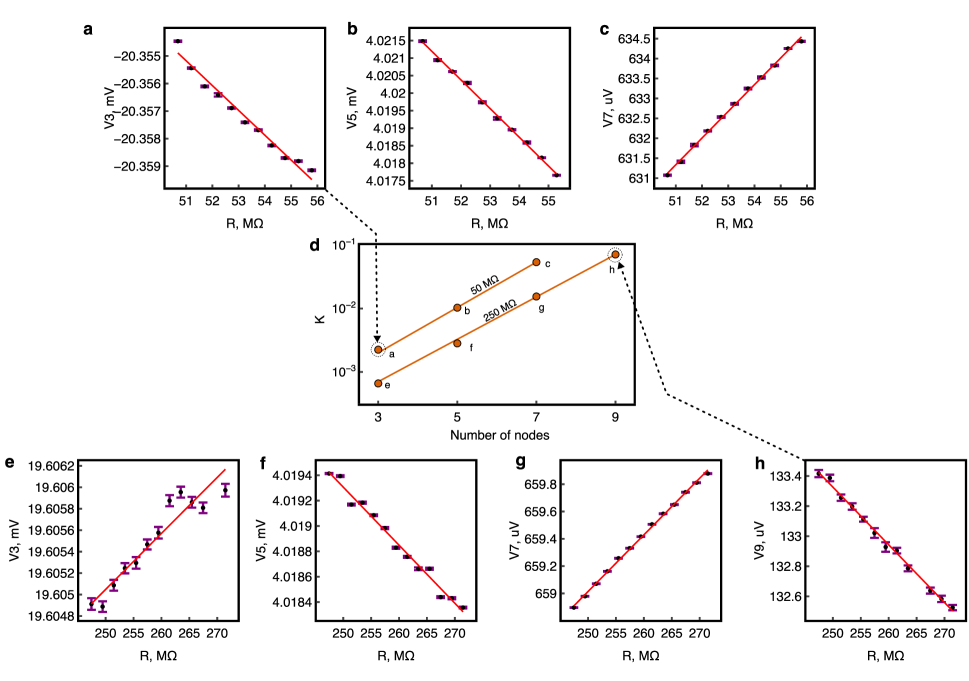
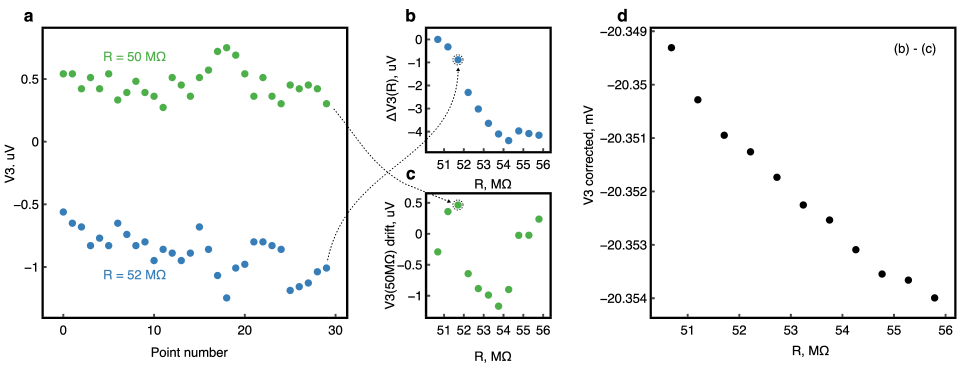
Figure M3 demonstrates the measurement steps involved in obtaining Fig. M2a. For each , the voltage is calculated as an average over data points taken seconds apart for a ms integration time. This averaging process is shown in panel Fig. M3a, which highlights the data points used to obtain one of the points in panel Fig. M3b. Additionally, to take into account the slow voltage drift that occurs during the time span of the measurement, we measure the voltage with a reference resistance (50 M, 200 M or open circuit for the different measurements shown in this work) just after reading the voltage with . This drift voltage is shown in Fig. M3c and is subtracted from the data shown in panel Fig. M3b data to obtain the values displayed in Fig. M3d, which is then used to calculate the value of for the given range of .