Excitonic interplay between surface polar III-nitride quantum wells and MoS2 monolayer
Abstract
III-nitride wide bandgap semiconductors exhibit large exciton binding energies, preserving strong excitonic effects at room temperature. On the other hand, semiconducting two-dimensional (2D)materials, including MoS2, also exhibit strong excitonic effects, attributed to enhanced Coulomb interactions. This study investigates excitonic interactions between surface GaN quantum well (QW)and 2D MoS2 in van der Waals heterostructures by varying the spacing between these two excitonic systems. Optical property investigation first demonstrates the effective passivation of defect states at the GaN surface through MoS2 coating. Furthermore, a strong interplay is observed between MoS2 monolayers and GaN QW excitonic transitions. This highlights the interest of the 2D material/III-nitride QW system to study near-field interactions, such as Förster resonance energy transfer, which could open up novel optoelectronic devices based on such hybrid excitonic structures.
keywords:
MoS2, GaN, surface quantum wells, cathodoluminescence, FRETLASPE]
Laboratory of Advanced Semiconductors for Photonics and Electronics (LASPE)
\phone+41 (0)21 693 45 33
LQP]
Laboratory of Quantum Physics (LQP)
École Polytechnique Fédérale de Lausanne (EPFL), CH-1015 Lausanne, Switzerland
LASPE]
Laboratory of Advanced Semiconductors for Photonics and Electronics (LASPE)
LASPE]
Laboratory of Advanced Semiconductors for Photonics and Electronics (LASPE)
LQP]
Laboratory of Quantum Physics (LQP)
École Polytechnique Fédérale de Lausanne (EPFL), CH-1015 Lausanne, Switzerland
LASPE]
Laboratory of Advanced Semiconductors for Photonics and Electronics (LASPE)
1 Introduction
Since the breakthroughs of blue light-emitting diodes (LEDs) in the 1990s 1, III-nitrides have emerged as a major family of contemporary semiconductors. This development is attributed to their remarkable optoelectronic properties, including a direct bandgap spanning from the near infrared to the deep ultraviolet, thermal and chemical robustness, and large exciton binding energies 2, which ensures strong excitonic effects 3, with for instance, the achievement of room temperature (RT) polariton lasing 4.
The isolation of graphene in 2004 5 marked the inception of a new era in solid-state physics. Owing to the weak interlayer van der Waals (vdW) interactions, layered materials can be easily exfoliated into atomically thin layers, \latini.e., two-dimensional (2D) materials, and seamlessly integrated with other materials, granting notable flexibility in constructing vdW heterostructures. Among various 2D materials, semiconducting transition-metal dichalcogenides (TMDs), such as MoS2, exhibit a sizeable bandgap 6 and strong light-matter coupling 7, making them highly desirable for optoelectronic applications. When the layer thickness is reduced to the atomic scale, carriers in 2D TMDs exhibit excitons with binding energies typically one to two orders of magnitude larger than those observed in conventional semiconductors 8, which ensures robust excitonic features at RT 9.
Mixed-dimensional vdW heterostructures combining TMDs with III-nitrides have already been proposed for a diverse range of applications including LEDs 10, water splitting 11, and photodetection 12. In such heterostructures, III-nitrides are typically utilized in bulk form. A closer look at TMD/III-nitride interactions requires the study of the exitonic interplay at the vdW interface only. However, conventional semiconductor surfaces possess deep states in the bandgap which act as non-radiative recombination centers (NRCs). These NRCs can effectively suppress excitonic features near the surface 13. In contrast to other III-V semiconductors, III-nitrides exhibit relatively low surface recombination velocity 14. In addition, by carefully designing the quantum well (QW) structure, the exciton binding energies can be further increased compared to those in bulk materials 15. Moreover, wurtzite III-nitrides exhibit large polarization mismatches at heterointerfaces 16, which results in a strong built-in electric field in the well and thereby large electron-hole dipoles in the QW. Then, 2D TMD excitons in their vicinity should enable dipole-dipole coupling, known as Förster resonance energy transfer (FRET) 17. This effect has been observed between CdSe/ZnS nanocrystals and surface InGaN QWs and could be utilized for developing highly efficient “energy-transfer color converters” 18.
In this study, we tune the excitonic interaction between 2D MoS2 and surface polar GaN/AlGaN QWs by varying the distance, , between the two. Cathodoluminescence (CL) measurements on bare QWs show appreciable emission at RT even in the absence of a surface barrier, which confirms a low surface recombination rate. Upon coating the surface with MoS2, the CL intensity markedly changes, indicating that deep traps still exist at the surface and are passivated by the MoS2 coating. Eventually, CL results from the sample with nm unveil a pronounced change of the emission at QW excitonic transitions upon monolayer (ML)-MoS2 deposition. This phenomenon points out the role of FRET between ML-MoS2 and surface GaN QW.
2 Results and Discussion
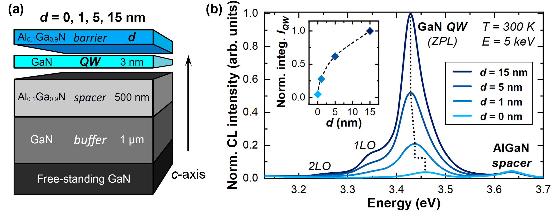
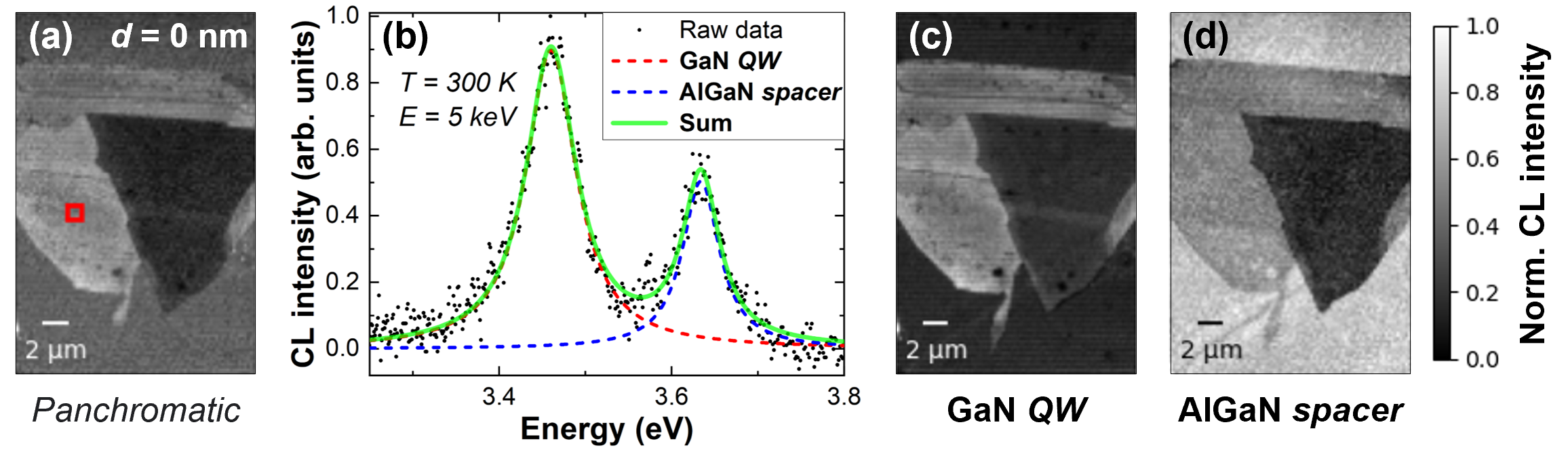
The sample structure of -axis oriented surface GaN/AlGaN QWs is illustrated in Fig. 1(a). The well thickness of 3 nm is chosen as a compromise between maximizing the binding energy and maintaining the dipolar nature of excitons 15. The sample without the AlGaN surface barrier is considered a “QW ” with nm. A 500 nm thick AlGaN spacer is inserted beneath the QW to prevent electron-beam-generated carriers from reaching the buffer where they could give rise to parasitic luminescence (Supporting Information (SI) Sec. 2). The CL spectra of surface QWs are presented in Fig. 1(b), with dominant peaks at eV and eV, attributed to the GaN QWs and AlGaN spacers, respectively. The first important observation is that, in contrast to near-surface GaAs QWs 13, all present GaN QWs exhibit a strong emission at RT, even in the absence of a surface barrier (SI Sec. 3).
Now we will delve into the characteristics of each CL peak. As the thickness of the surface barriers is smaller than the carrier diffusion length in Al0.1Ga0.9N 19, it is reasonable to assume that most of the carriers generated in the surface barrier diffuse to the QW where they recombine. Hence, the AlGaN emission in Fig. 1(b) originates from the spacer that is farther away from the surface, where carriers recombine before reaching the QW. The depth of the interaction volume of the 5 keV electron beam in these samples is more than 100 nm (SI Sec. 2), which implies that the total carrier generation rate remains nearly constant regardless of the position of the QW in the surface region, \latini.e., . This is corroborated by the comparable AlGaN peak intensity in all samples (SI Sec. 3). On the other hand, the GaN QW peak changes markedly with . In contrast to other surface QWs, the peak of the uncapped well ( nm) blueshifts by meV. This can be explained by a stronger carrier quantum confinement imposed by the free surface (SI Sec. 3). The integrated QW intensity (see SI Sec. 3 for calculation details) in Fig. 1(b) exhibits a nonlinear increase with increasing , which indicates a reduction of non-radiative recombination channels. For a -plane (Al)GaN surface, a high density of deep levels can act as effective NRCs 20. Thus, carriers in surface QWs can tunnel through the nanoscale barrier and be captured by surface traps (STs). The -dependent QW intensity can be modeled by an exponential function to account for carrier tunneling 13 (SI Sec. 3). Therefore, the nonlinear increase in QW emission with increasing demonstrates the significant impact of STs on surface GaN QWs, despite the typically low surface recombination velocity usually ascribed to III-nitrides. This highlights the importance of surface passivation for III-nitrides, particularly in devices with a high surface-to-volume ratio 21.
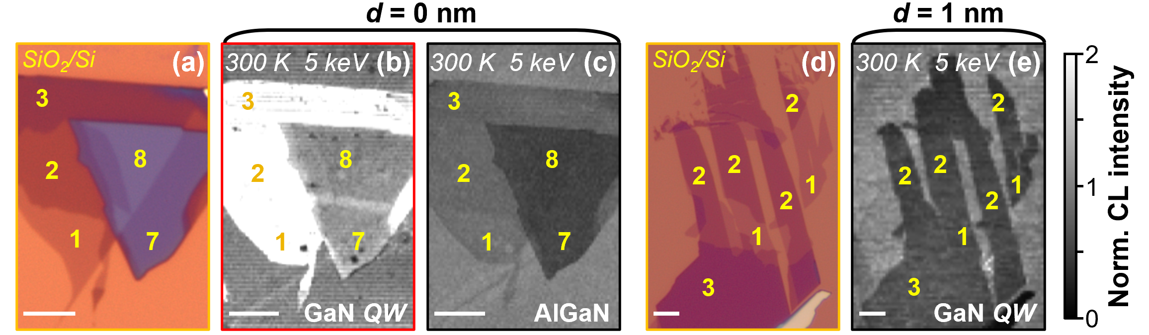
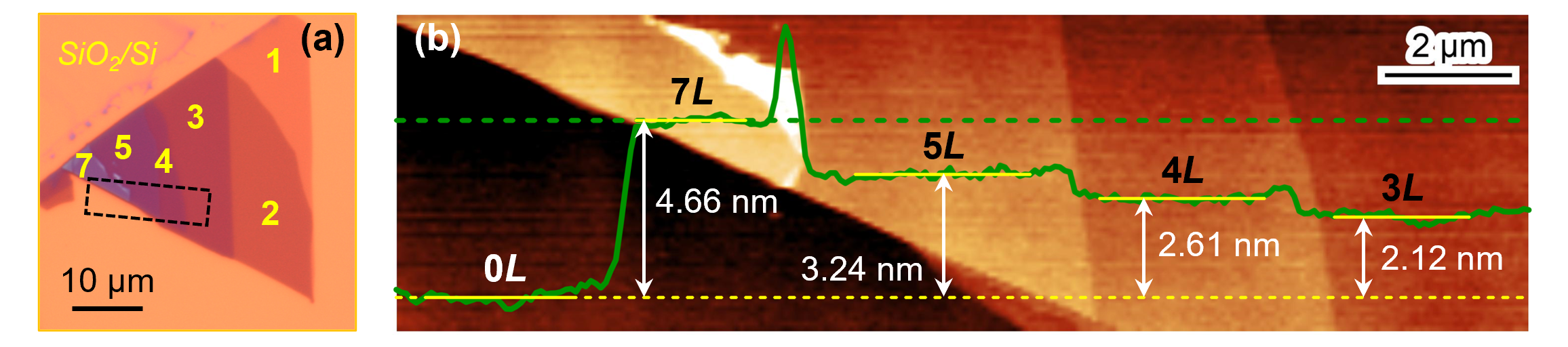
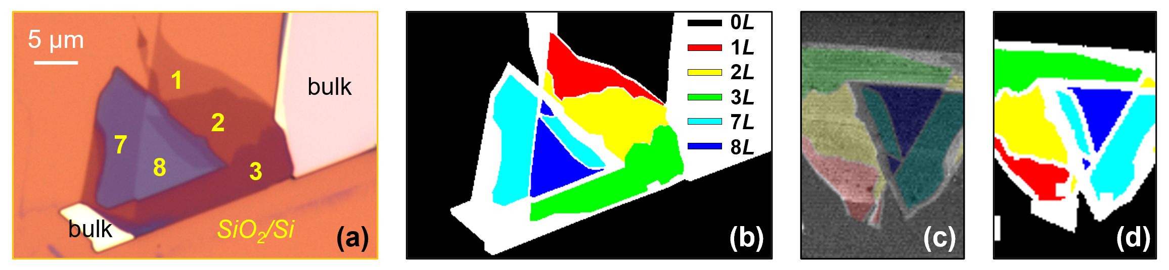
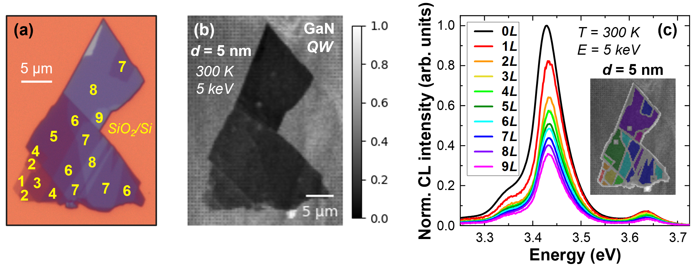
Mechanically exfoliated MoS2 flakes were prepared on a SiO2/Si substrate, where the contrast in an optical microscope is highly sensitive to MoS2 thickness due to light interference 22 (Figs. 2(a, d)). After precise characterization of the layer thickness (SI Sec. 4), the selected flakes were deposited on the surface GaN QWs. Hyperspectral CL maps were acquired on the MoS2 flake regions. Each pixel in the map corresponds to the CL at that position and the associated spectrum was fitted to generate integrated intensity maps of the GaN QW and AlGaN emissions (SI Sec. 5). To facilitate the comparison, all intensity maps were normalized by the average intensity of the background (SI Sec. 5).
Among all intensity maps, the uncapped GaN QW ( nm) shows a peculiar behavior: the region covered by MoS2 exhibits a strongly enhanced emission (Fig. 2(b)). This is not consistent with the high spectral absorptance of MoS2 in the range of (Al)GaN emission ( of the incident light is absorbed by ML-MoS2) 23. In contrast, the AlGaN intensity map extracted from the same sample shows a decrease in intensity with increasing MoS2 thickness (Fig. 2(c)), as expected from absorption 24. Additionally, when the GaN QW is slightly moved away from the surface, \latini.e., nm, its CL intensity is also reduced with the presence of MoS2 (Fig. 2(e)). It is noteworthy that, despite similar MoS2 spectral absorptance in the corresponding energy ranges, the contrast observed from the GaN QW with nm differs from that of the AlGaN emission (Fig. 2(c)). The former shows a more pronounced reduction in intensity throughout the entire region covered by MoS2 of MLs. The underlying reason will be elucidated later. On the other hand, considering the abnormal increase in CL intensity linked to MoS2 for the uncapped QW, it is evident that only the emission of the layer in direct contact with the MoS2 flake is enhanced, indicating that the MoS2-enhanced GaN emission is associated with surface passivation.
To confirm this hypothesis, we performed CL experiments on a GaN epilayer coated by MoS2 (SI Sec. 6). The CL map also exhibits an increase in GaN emission in the presence of MoS2, albeit weaker compared to the case of the uncapped GaN QW. This is consistent with a surface passivation effect: in a GaN epilayer, CL emission comes from both the surface and bulk regions, which diminishes the surface impact.
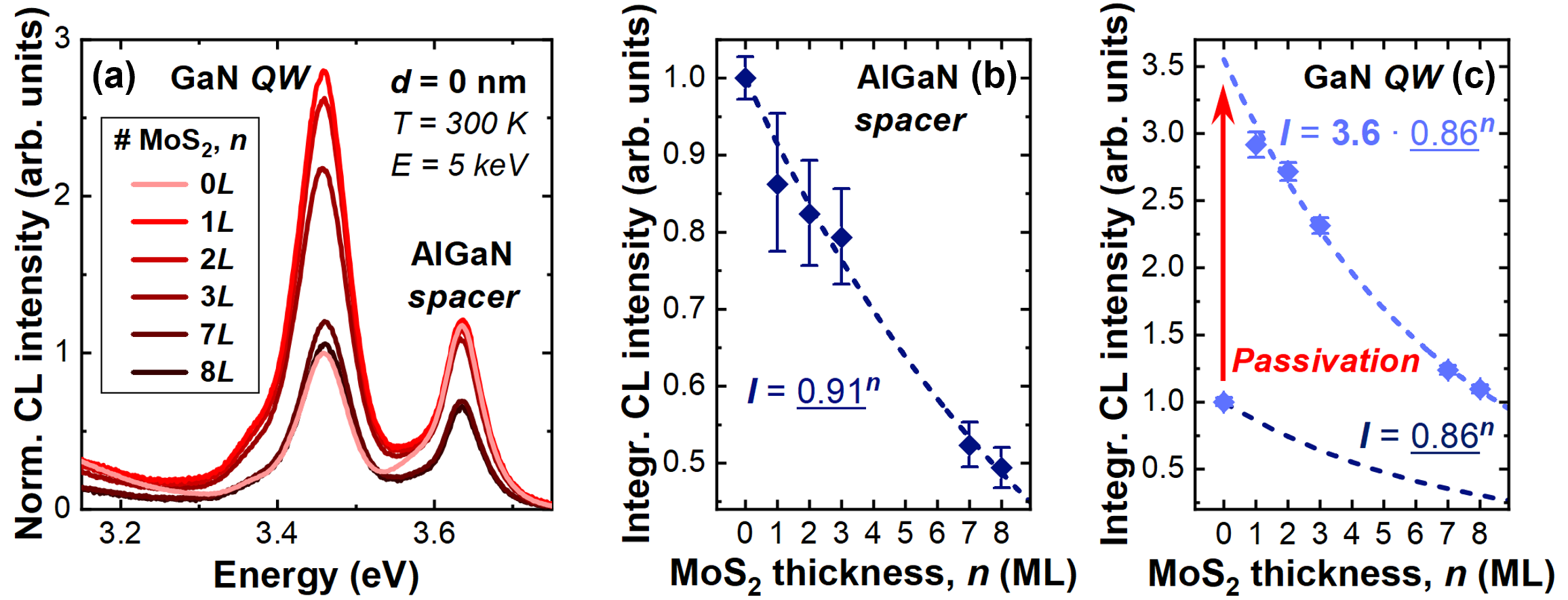
In order to obtain more quantitative information from the results of the uncapped QW, average CL spectra were extracted from regions with different MoS2 thicknesses (SI Sec. 5), as shown in Fig. 3(a). These spectra were deconvoluted to derive the integrated intensities of the GaN QW and AlGaN spacer peaks, respectively (SI Sec. 3). Let us consider first the AlGaN spacer emission, which is not affected by any surface effects (Fig. 3(b)). It exhibits a monotonic decrease with increasing MoS2 thickness, as expected from absorption. It is important to note that the presence of MoS2 has a negligible impact on carrier injection into the samples, primarily due to the limited interaction of the electron beam with these ultra-thin layers 25. To model the AlGaN intensity decrease, we consider that the interlayer coupling in MoS2 does not strongly influence the absorption, thus the absorption in each ML is nearly the same. Therefore, the normalized intensity can be fitted with a power function: , where is the number of MoS2 MLs and is the absorptance in each ML. The fit gives , which agrees with the absorptance measured in ML-MoS2 at 3.63 eV 23, \latini.e., the peak energy of AlGaN emission. Similarly, Fig. 3(c) shows the plot of the GaN QW CL intensity as a function of MoS2 thickness. Fitting the data with the same absorption model reproduces the overall trend, with , matching ML-MoS2 absorptance at 3.45 eV 23. However, this fit does not capture the experimental data at , instead predicting an intensity 3.6 times higher than the measured value. This indicates that the deposition of the first ML-MoS2 results in a strong increase in the surface emission, \latini.e., the emission of the uncapped QW, due to single ML-MoS2 surface passivation effect.
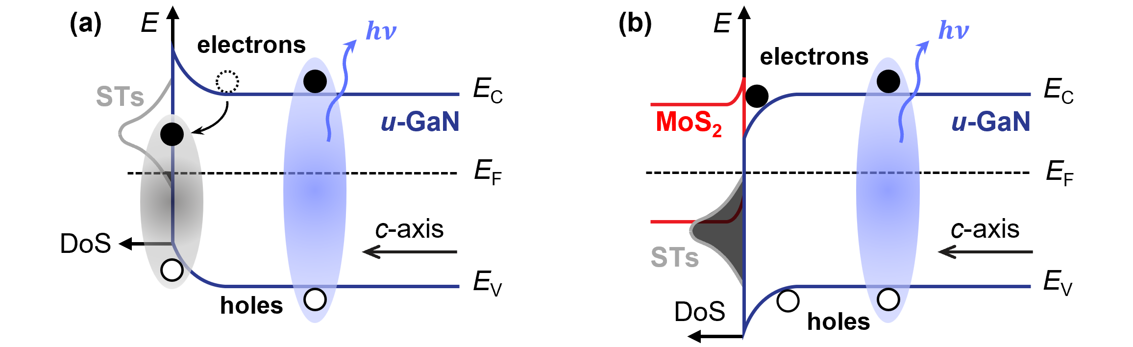
A possible explanation for surface passivation is based on type-II band alignment between MoS2 and GaN 12: the unintentionally doped GaN surface exhibits an upward surface band bending due to the presence of STs (Fig. 4(a)); with MoS2 deposited on the surface, charge transfer between the two materials leads to an upward band bending in MoS2 and a downward band bending in GaN (Fig. 4(b)). Consequently, STs are occupied and are no longer capable of trapping excitons in the surface region, therefore, surface emission is markedly enhanced.
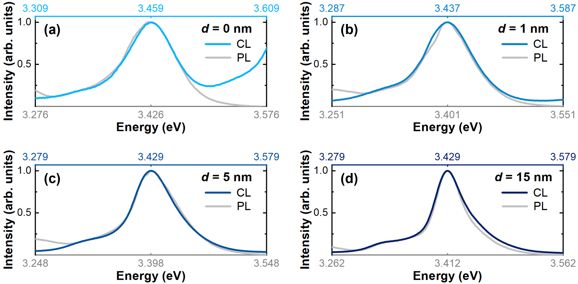
As the deposition of MoS2 exerts a significant impact on the emission of the uncapped QW, it is not a suitable sample for studying excitonic interplay between the two materials. Conversely, in the sample with nm, carriers confined in the well are no longer interacting with STs (SI Sec. 3), making this system ideal for gaining insight into the excitonic interactions. The CL spectra with different MoS2 thicknesses are displayed in Fig. 5(a). Throughout the entire detection range, from eV to eV, the CL intensity decreases with increasing MoS2 thickness. This energy range coincides with the C-absorption band of ML-MoS2 23. Interestingly, for all peaks related to the GaN QW emission, including the ZPL and its LO phonon replicas, the intensity difference between ML-MoS2 capped QW () and bare QW () is notably larger than the intensity change observed when increasing the MoS2 thickness by 1 ML.
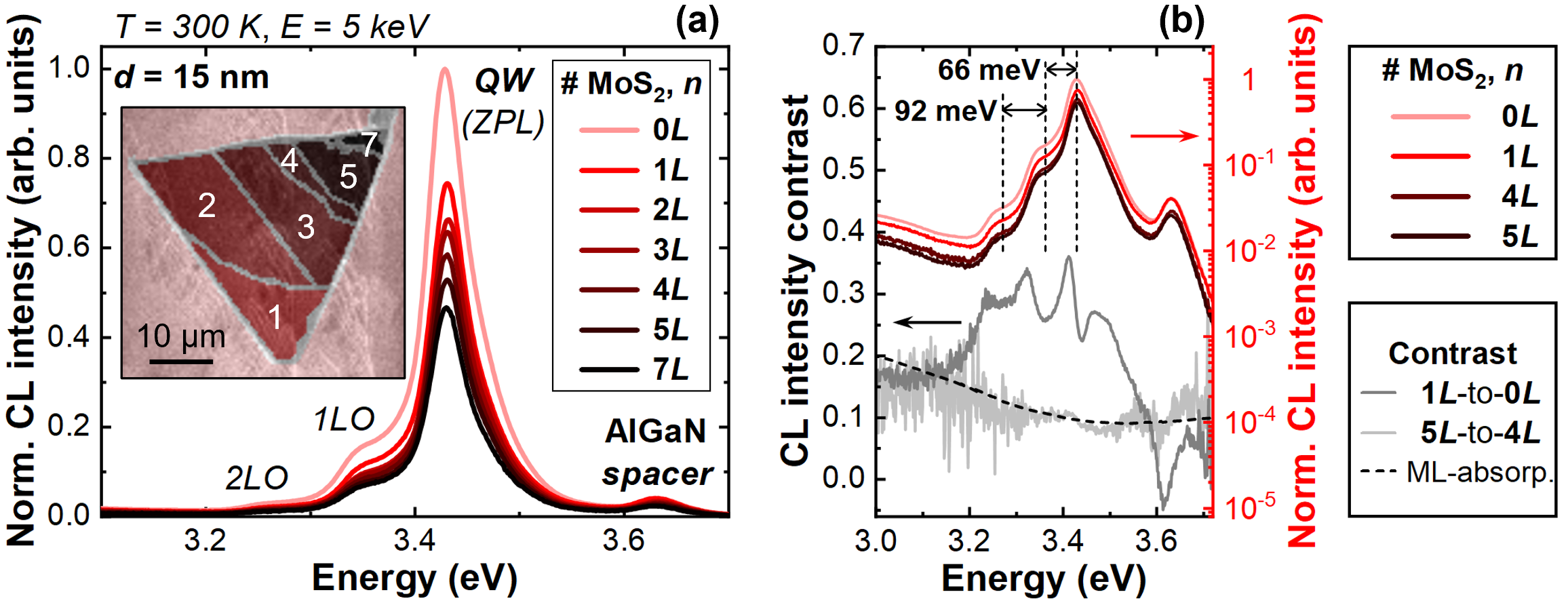
To get a deeper insight into the influence of MoS2 on the QW emission, we computed the intensity contrast, following the formula:
where is the CL intensity of the region covered by -MoS2, \latini.e., MoS2 of MLs, as a function of photon energy, . As depicted in Fig. 5(b), the intensity contrast between regions covered by - and -MoS2 (light grey curve) aligns with the reported ML-MoS2 spectral absorptance 23 (black dashed curve). On the contrary, the contrast between the background and the -MoS2 region (dark grey curve) exhibits a significant discrepancy in the emission range of GaN QW and AlGaN. In the range around the AlGaN bandgap, a peak with a negative contrast is observed, \latini.e., higher AlGaN emission in the presence of ML-MoS2. This can be explained by the surface passivation induced by ML-MoS2, which enhances surface emission from the AlGaN barrier (SI Sec. 7). In the range of GaN QW emission, multiple peaks, with contrasts much higher than expected from absorptance only, are observed. The dominant peak at 3.41 eV, along with the two lower-energy peaks, can be associated with the ZPL and the corresponding LO phonon replicas of the GaN QW emission in the CL spectrum (light red curve). The carrier density in the well is on the order of (SI Sec. 2). This is close to the critical carrier density of the Mott transition reported for similar GaN QWs 26, 27. Therefore, CL peaks of the GaN QW can arise from two possible physical origins: excitonic transitions or electron-hole plasma emission. The presence of excitonic features in the well can be confirmed by the energy spacing between adjacent peaks of the QW emission. Theoretically, the peak emission energy of the th LO phonon replica of excitons can be expressed as 28:
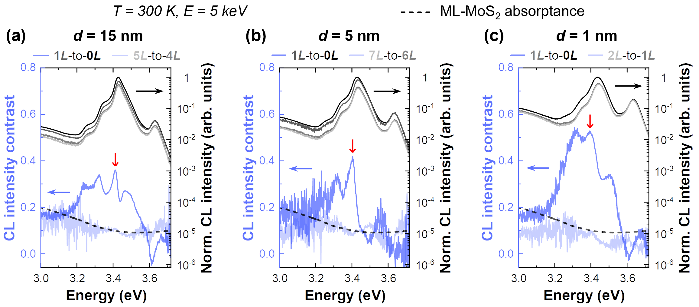
where is the peak energy of the ZPL, is the LO phonon energy (92 meV for GaN 29), and is the kinetic energy of the excitons, which depends on , the dimensionality of the system ( for excitons confined in a QW). is the lattice temperature, and is the Boltzmann constant. For excitonic emission from a GaN/AlGaN QW at 300 K, the theoretical energy spacing between the ZPL and the 1st LO phonon replica should be , \latini.e., 66 meV, whereas the energy spacing between the 1st and 2nd LO phonon replicas should be , \latini.e., 92 meV. This agrees perfectly with the CL spectra shown in Fig. 5(b), which confirms the excitonic nature of the QW emission. Furthermore, the CL emission profile of the GaN QWs is compared to the emission measured by photoluminescence (PL) using a continuous wave (cw) 325 nm laser with a power density of W/cm2, which results in much lower carrier injection into the QWs (SI Sec. 3). Although the energy peak blueshifts in CL, which may be attributed to the screening of the built-in field at higher carrier density, the line shape remains nearly unchanged. This observation excludes Fermi filling of continuum states, characterized by a strong extension of the high-energy tail, which is typically observed beyond the Mott transition 26. Therefore, our findings demonstrate that, besides the conventional absorption, there is an additional energy transfer channel between the GaN QW and ML-MoS2, in resonance with the excitonic transitions in the QW. Such an effect is clearly observed in the contrast induced by the direct deposition of ML-MoS2 on the QW surface.
The relevant mechanism is probably FRET, which provides an efficient energy transfer between energy “donor” and “acceptor” materials through non-radiative dipole–dipole coupling 17. In our case, carriers confined in the polar GaN/AlGaN QW are subjected to a built-in field, forming dipoles which act as energy “donors”. On the other hand, different from excitons in other MoS2 layers, excitons in the ML-MoS2 on the surface are the closest to the QW dipoles and experience a weaker dielectric screening due to the absence of a layer on top. Furthermore, since the AlGaN surface barrier possesses a polar nature as all III-nitride layers grown along the -axis, it can enhance the dipolar characteristics of the excitons in direct contact with it. All these result in strong dipoles in ML-MoS2, which act as energy “acceptors”. The associated donor-acceptor distance () is nm, which is on the order of the typical range for FRET 30, 31, 32. Therefore, we attribute the observed sharp peaks with intensity contrasts as high as to the strong dipolar coupling between excitons in the QW and in ML-MoS2 in the near-field regime. This effect also explains the difference in CL contrast between the AlGaN emission from the uncapped QW (Fig. 2(c)) and the GaN QW emission from the sample with nm (Fig. 2(e)). Specifically, the AlGaN emission originates from the bulk region where the excitonic feature is weaker and is larger. In contrast, the GaN QW emission with nm is associated with strong excitonic effect in the well, localized very close to MoS2. As a result, a significant quenching of the emission is observed due to efficient FRET. The peak QW intensity contrast induced by ML-MoS2 on the sample with nm is (SI Sec. 8), much higher than the 36 observed for nm. This difference is consistent with the strong dependence of FRET on . It is important to note that with a thin surface barrier of 1 nm, the QW emission is still strongly influenced by STs (SI Sec. 3). The deposition of ML-MoS2 should simultaneously cause a negative contrast due to surface passivation. Therefore, the 52 contrast deduced from CL measurements is likely underestimated.
3 Conclusion
In summary, we investigated the optical properties of a series of surface GaN/AlGaN QWs with variable nanometer-scale surface barrier thickness, to 15 nm. Thanks to the low surface recombination rate, high CL intensity was observed, even from the uncapped QW ( nm). The QW intensity increased nonlinearly with increasing , showing the non-negligible impact of deep traps existing at III-nitride surfaces. Using these surface GaN QWs as substrates, we deposited MoS2 flakes of a few MLs. The presence of MoS2 enhanced the emission from the uncapped QW, demonstrating III-nitride surface passivation using 2D material coating. For the QW with nm, unaffected by STs, a strong excitonic interaction between the GaN QW and ML-MoS2 is observed. This effect is attributed to a strong dipole-dipole coupling, \latini.e., FRET, between the excitons of the two materials. Our results highlight the potential of surface III-nitride QWs as a platform for investigating the near-field interplay between 2D materials and III-nitrides, which could be applied to develop novel optoelectronics based on such hybrid heterostructures.
4 Supporting Information
The Supporting Information accompanies this paper. Further details on:
- 1.
- 2.
- 3.
- 4.
- 5.
- 6.
- 7.
- 8.
The authors thank Dr. R. Butté (EPFL) for useful discussions. The Interdisciplinary Centre for Electron Microscopy (CIME) at EPFL is acknowledged for access to its facilities. M. B. acknowledges the support of SNSF Eccellenza grant No. PCEGP2_194528, and support from the QuantERA II Programme that has received funding from the European Union’s Horizon 2020 research and innovation program under Grant Agreement No. 101017733.
SUPPORTING INFORMATION
5 1. Experimental methods
Sample growth. The samples used in this study were grown by metalorganic vapor phase epitaxy in a horizontal Aixtron 200/4 RF-S reactor on commercial -plane free-standing GaN substrates with very low dislocation density, typically a few . The growth process can be divided into two parts. First, a rapid growth of the GaN buffer and a nm Al0.1Ga0.9N spacer is conducted at a growth rate of m/h and a temperature of 1000 °C. Trimethylgallium and trimethylaluminum are used as precursors, and H2 is used as carrier gas. Then, the growth rate is lowered to 60 nm/h at a temperature of 800 °C for the single QW region, which includes a 5 nm Al0.1Ga0.9N barrier, the 3 nm GaN QW layer, and the Al0.1Ga0.9N surface barrier. This low-temperature (LT) growth is intended to mitigate large-scale Al content fluctuations within the barriers, thereby minimizing the inhomogeneous broadening of the QW emission 33. For the LT growth, the metalorganic source for gallium is changed to triethylgallium, and the carrier gas is switched to N2. The entire structure is grown without any intentional doping.
Fabrication of MoS2-on-(Al)GaN heterostructures. The MoS2 flakes were obtained through the well-known “scotch-tape” mechanical exfoliation method 5 and deposited on a 10-minute oxygen-plasma-etched SiO2/Si substrate. The precise thickness of the selected MoS2 flakes was determined by optical microscopy, atomic force microscopy (AFM) and Raman spectroscopy (SI Sec. 4). Following the characterization, the selected flakes were picked up and transferred onto the cleaned surface of the (Al)GaN samples (QWs and a bulk GaN epilayer) using a dry transfer technique 34, 35. Initially, a high-quality uniform stack of poly(bisphenol A carbonate)/polydimethylsiloxane was prepared on a glass slide. This stack was then mounted on a homemade transfer stage to pick up MoS2 at 70 °C. Subsequently, the MoS2 flake was transferred to the surface of the (Al)GaN sample at 150 °C. Finally, the entire sample was immersed in chloroform to clean its surface.
Cathodoluminescence spectroscopy. CL imaging was conducted using a specialized scanning electron microscope system (Attolight Rosa 4634) with an acceleration voltage of 5 kV. A Cassegrain reflective objective was employed to collect the emitted light, which was subsequently directed to a spectrometer equipped with a 600 lines per mm grating with a blaze wavelength of 300 nm. The dispersed light was then captured by a cooled charge-coupled device camera, enabling the recording of a full intensity-energy spectrum at each pixel, \latini.e., hyperspectral imaging.
6 2. Estimation of the carrier density in the QWs
The interaction volume of a 5 keV electron beam at 300 K in bulk Al0.1Ga0.9N is determined through Monte Carlo simulation (CASINO) 36, as depicted in Fig. S1(a). For this simulation, an electron beam containing electrons was used, with a spot size of 25 nm, and an accelerating voltage of 5 kV. This can be deemed representative of all the samples examined in this study, as the thickness of the GaN QW is negligible compared to the overall interaction volume, and a variation in Al content leads to less than change in mass density. Based on the simulation, the normalized energy deposited in the sample is plotted as a function of depth from the surface (Fig. S1(b)), which indicates that most of the beam energy is absorbed within a 150 nm region from the surface. Considering that the minority carrier diffusion length in GaN and Al0.1Ga0.9N is typically limited to 100 nm at RT 37, 19, the 500 nm thick Al0.1Ga0.9N spacer serves as an effective barrier which prevents beam-generated carriers from reaching the GaN buffer. Consequently, the observed GaN emission in all the samples is attributed solely to the GaN QWs.
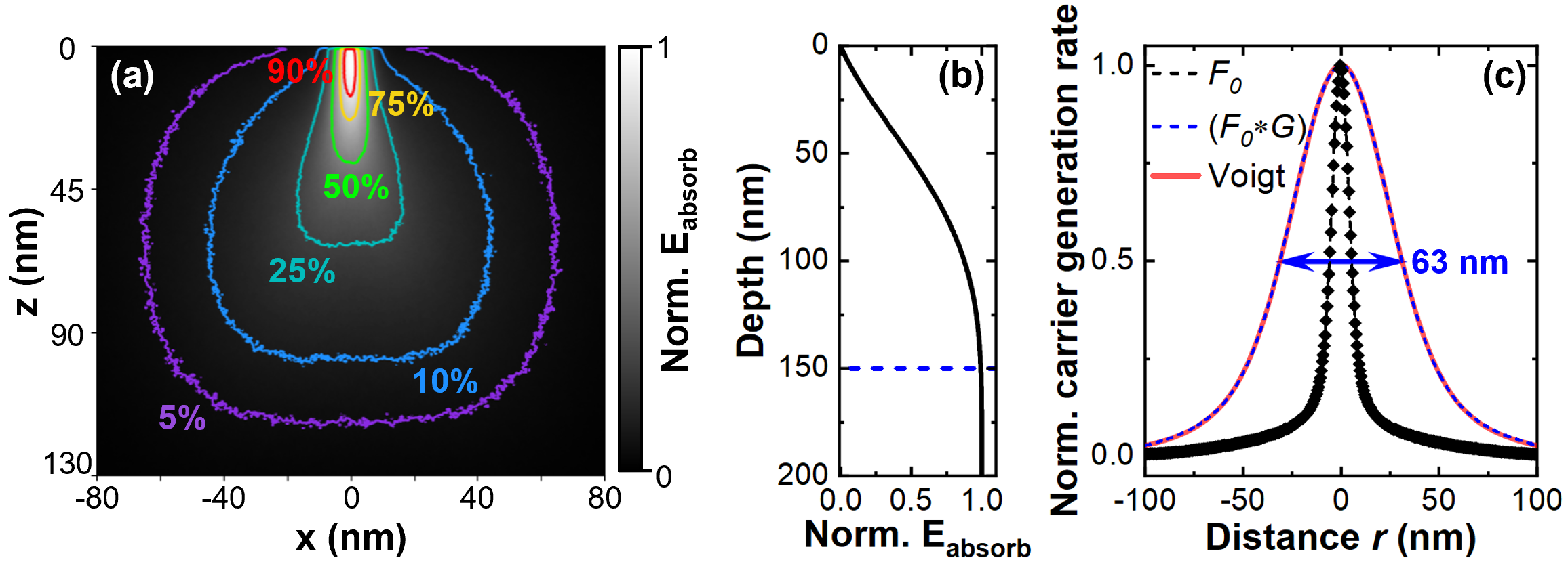
To estimate the carrier density in the QWs (), we first compute the lateral carrier generation rate distribution , where represents the lateral distance to the beam center using cylindrical coordinates. This is achieved by convolving the carrier generation rate distribution , deduced from the simulation, with a Gaussian distribution . Specifically, is obtained by summing the deposited energy over the direction, assuming that all carriers relax to the QW. is characterized by a standard deviation nm, which accounts for the broadening caused by carrier thermalization at 300 K 38. The resulting profile is normalized by its peak value at and fitted by a Voigt function, yielding a full width at half maximum (FWHM) of nm (Fig. S1(c)). It is important to note that our estimation does not consider the lateral carrier diffusion occurring in the surface barrier before carriers completely relax to the QW. As a result, the calculated FWHM underestimates the actual broadening of the carrier generation rate distribution in the QW. Meanwhile, the total generation rate, (s-1), of carriers in CL can be estimated using the well-known equation 39:
| (1) |
where is the electron beam probe current, is the charge of an electron, is the average energy deposited per electron in the sample, and is the bandgap of the sample. is calculated as the difference between the beam energy () and the energy lost through backscattered electrons (). In our case, to 233 pA, measured using a Faraday cup attached to the sample holder, eV for Al0.1Ga0.9N at 300 K 40, keV, and keV computed via Monte Carlo simulation. Assuming that all generated carriers relax to the QW, the carrier generation rate in the QW, , is around to s-1. Under the assumptions of carrier lifetime being independent of carrier density and no carrier diffusion in the QW, the maximal carrier density in the QW at can be calculated as:
| (2) |
with representing the carrier lifetime, which is typically around 1 ns for GaN/Al0.1Ga0.9N structures at RT 41, 42. Hence, the estimated maximum carrier density in the QWs is approximately to cm-2. It should be noted that this value may be overestimated, considering the broader actual carrier distribution, as discussed previously. Additionally, our assumption that all carriers relax to the QW might not hold true in practice. As a result, the average carrier density in the QWs is expected to be on the order of cm-2.
7 3. Optical properties of surface GaN QWs
Since the QW emission varies significantly with the surface barrier thickness, , CL spectra of the surface GaN QWs are presented in logarithmic scale in Fig. S2(a), which improves the visibility of lower-intensity peaks. It is evident that, unlike surface GaAs QWs 13, the emission intensity from our surface GaN QWs remains considerably strong even in the absence of a surface barrier. In this logscale plot, the AlGaN spacer emission from all the samples exhibits almost identical intensity. This confirms that the injection level into the samples is nearly the same, unaffected by the varying .
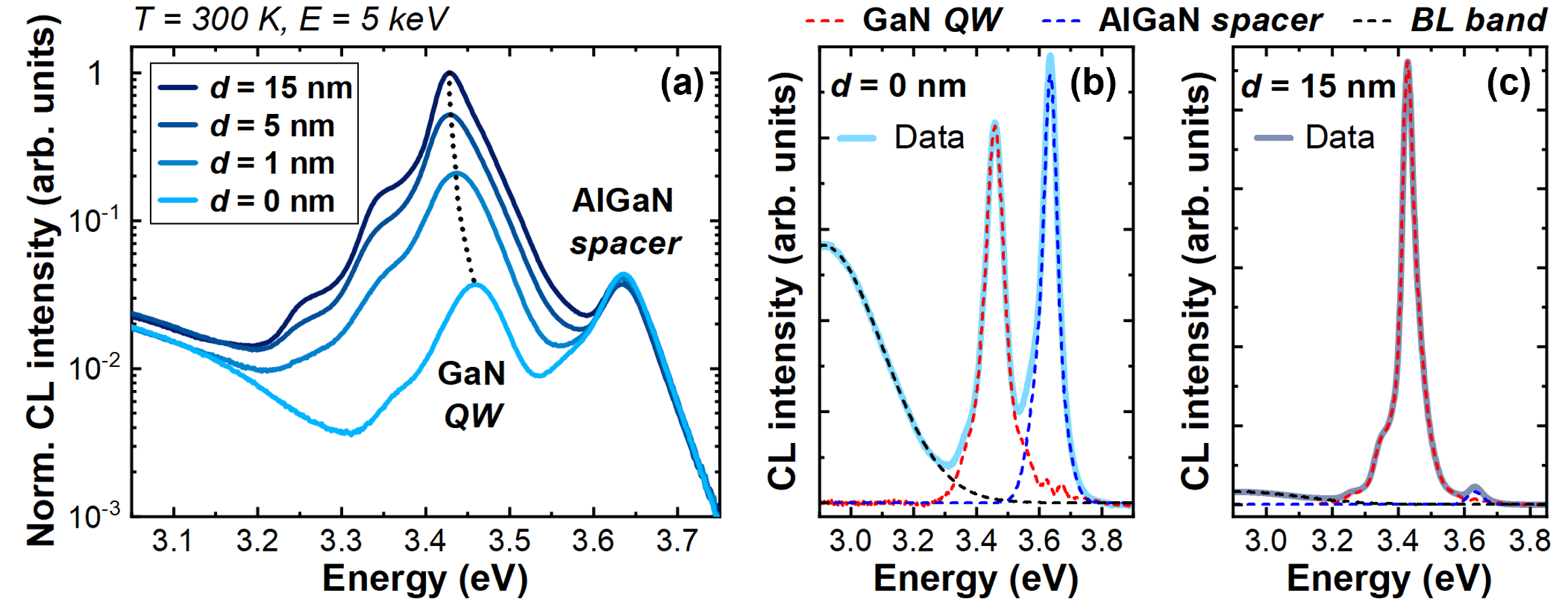
For all the CL spectra analyzed in this study, a spectral deconvolution is conducted to extract detailed information of the GaN QW and AlGaN spacer emissions (Figs. S2(b, c)), in particular the peak energy and integrated intensity. The spectral deconvolution begins with a preliminary multi-peak fitting aimed at extracting the line shapes of the AlGaN emission and the background defect emission, \latini.e., the broad blue luminescence (BL) band peaking at eV 43. However, for the GaN QW emission, which includes the ZPL and multiple LO phonon replicas, achieving an accurate fit is challenging. To address this, we deduced the QW emission by subtracting the fitted BL band and AlGaN emission from the raw data. This approach ensures a uniform treatment for all spectra, maintaining effective deconvolution of the overlapping QW and AlGaN emissions (Fig. S2(b)) while preserving the precise line shape of the entire QW emission (Fig. S2(c)). All the error bars in integrated intensity are estimated from the preliminary multi-peak fitting.
| d | 0 nm | 1 nm | 5 nm | 15 nm |
|---|---|---|---|---|
| GaN QW | 3.459 eV | 3.437 eV | 3.429 eV | 3.429 eV |
| AlGaN spacer | 3.635 eV | 3.635 eV | 3.635 eV | 3.633 eV |
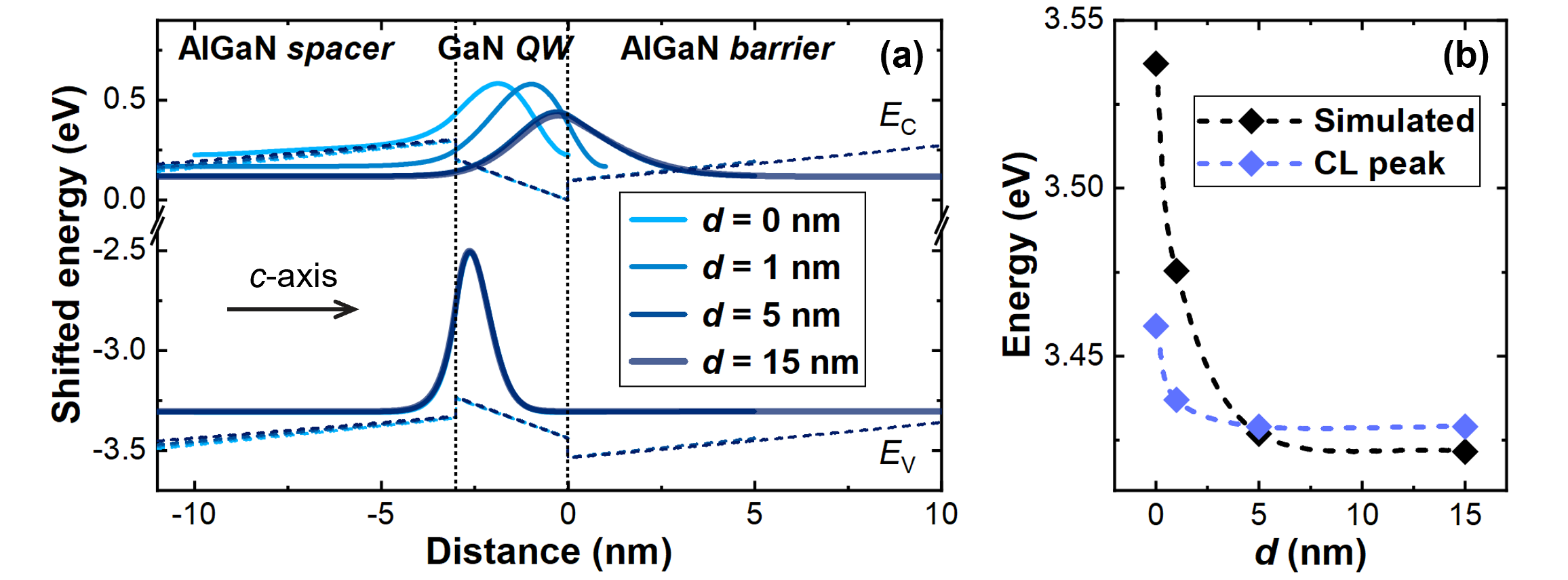
The peak energies of the surface GaN QWs are presented in Table 1. Notably, the peak energy of the AlGaN spacer emission remains nearly constant across all samples. In contrast, the GaN QW peak exhibits a small blueshift for the sample with nm and an even larger blueshift for the uncapped QW ( nm). To gain insights into these observations, we conducted band diagram calculations and analyzed the corresponding confined states using the commercial software, nextnano 44, as shown in Fig. S3(a). For these polar surface QWs, the presence of the free surface restricts the electron wavefunction penetration into the surface barrier, which leads to enhanced quantum confinement of carriers in the well when is small. To further analyze the emission energy as a function of , we compared the simulated interband transition energies with the GaN QW peak energies extracted from CL measurements (Fig. S3(b)). While the overall -dependent trends are in agreement, the simulated values for QWs with nm are much higher than the experimental data. This disparity arises from the Dirichlet boundary condition applied at the free surface in the simulation, which does not consider the evanescent wave in the vacuum, thus leading to an overestimation of the confinement energy induced by the free surface. Despite this discrepancy, the overall agreement between the two trends provides a reasonable explanation for the large blueshift observed in the uncapped QW: carrier quantum confinement in this “well” is significantly enhanced by the free surface.
In Fig. S4(a), the integrated QW intensity is plotted against , clearly demonstrating a nonlinear increase with increasing . However, this is contradictory to the simulation (Fig. S3(a)): for larger , the wavefunction overlap is smaller, thus the radiative recombination rate is lower. If the weight of non-radiative recombination was the same for all the samples, the QW emission intensity should decrease with increasing . Therefore, the observed increase in intensity is dominated by a reduction in non-radiative recombination channels. Given the relation to , these non-radiative channels are surface-related, \latini.e., STs.
Since the physics of the envelope function formalism fails in vacuum as there is no longer any Bloch function, we will not use the simulated wavefunctions for the comparison of the QW emission intensities. To model the -dependent QW emission intensity, we take into account the probability of carrier tunneling from the well to the surface 13, where carriers could potentially become trapped without emitting light, \latini.e., recombine non-radiatively. First of all, the measured QW emission intensity is correlated to the internal quantum efficiency of the sample, which is the ratio between the radiative recombination rate () and the effective recombination rate (). Given that these samples possess similar structures and were grown under identical conditions, and that their difference in confinement has a negligible impact on the emission, as previously discussed, it is reasonable to assume that in these QWs remains constant. Subsequently, the QW intensity should be inversely proportional to :
| (3) |
where represents the effective recombination rate in the absence of STs, \latini.e., QWs with very large . denotes the non-radiative recombination rate associated with STs, which can be expressed as:
| (4) |
where is the probability of a surface carrier being non-radiatively trapped by STs, and is the carrier Schrödinger wavefunction, with the distance measured along the -axis. Here, is defined at the QW-barrier interface. Hence, the integral of the probability density, , from to infinity, is associated with the probability of carrier tunneling from the well to the surface. In our case, due to the presence of the built-in field, electrons in the well are more likely to cross the barrier (Fig. S3(a)). Therefore, they are regarded as the main carriers responsible for the tunneling from the well to the surface. Assuming a similar, albeit minor, surface band bending across all samples, the barrier height for electrons in the QWs is approximately the conduction band offset, , between the GaN QW and Al0.1Ga0.9N barrier. This value can be estimated by considering the bandgap () at 300 K of GaN ( eV 40) and Al0.1Ga0.9N ( eV 40), along with the “common anion rule” 45: meV. The one-dimensional Schrödinger equation for an electron in the barrier can be written in the form:
| (5) |
Here is the reduced Planck’s constant and is the effective mass of the electron in Al0.1Ga0.9N ( 46, with the electron rest mass). The solution of the equation is in the form of an evanescent wave: , with a constant coefficient. By inserting this expression into Eq. 4, we obtain:
| (6) |
Given that all the samples exhibit comparable material quality, we can treat and as constants independent of the variable . Subsequently, by combining Eqs. 3 and 6, we can model the -dependent normalized QW intensity using the following formula:
| (7) |
Here , calculated using Eq. 5, and is a parameter that can be deduced from the data. The QW CL intensity in Fig. S4(a) is normalized by the value at nm, which aligns with the model, given that the term is at nm, using the previously calculated value of . As shown in Fig. S4(a), our model (black dashed curve) successfully captures most of the experimental data, except for the point at nm.
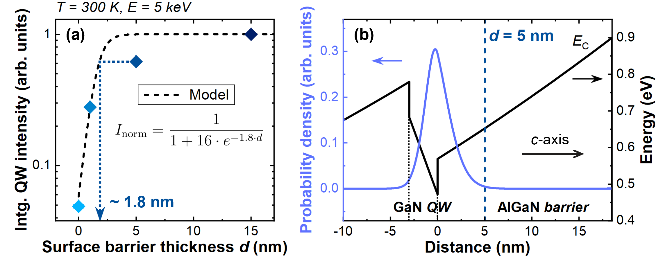
Indeed, if we compute the electron wavefunction probability density in a well with large (Fig. S4(b)), the penetration is no longer affected by the boundary condition at the free surface. Electrons confined in the well have a probability of less than 1 to tunnel through a 5 nm Al0.1Ga0.9N barrier (indicated by the dark blue dashed line). The observed increase in intensity when increases from 5 nm to 15 nm suggests that the effective thickness () of the 5 nm thick AlGaN barrier, acting as an “electron blocking layer”, is significantly smaller than its physical size. In fact, for the same intensity in the model’s curve, the corresponding barrier thickness is nm (indicated by the dark blue dotted arrow in Fig. S4(a)), \latini.e., nm less than the actual thickness. A possible explanation for this discrepancy is the presence of percolative paths in the AlGaN barrier caused by alloy disorder 47. The random distribution of Al atoms in the barrier results in regions of varying Al content, known as alloy disorder. In other words, if we consider the same Al content in the barrier, it implies that is locally changing. Since nm is at the limit of carrier tunneling (Fig. S4(b)), for regions where nm, there is no significant impact on the emission. However, in regions where nm, the intensity can be dramatically affected. Thus, the overall consequence of the percolative paths within the 5 nm thick AlGaN barrier is a reduction in . Considering the typical scale of alloy disorder in the III-nitride system, \latini.e., the average size of the Al-free regions in our case, is nm 48, the disorder-induced percolation effect is consistent with the observed difference between the physical and effective thickness for nm. Regarding the other two samples with smaller , fluctuations in both directions (decreasing and increasing ) lead to changes in the intensity. Therefore, the order of magnitude of the intensity for these samples is less affected by the percolation effect. As a result, unlike the sample with nm, the values of these samples align well with the model, as shown in Fig. S4(a).
To summarize the findings discussed so far, we model the -dependent QW intensity by considering the carrier tunneling effect, and deduce that the presence of alloy disorder in the AlGaN barrier reduces its effective thickness. This leads to surface-sensitive QW emission even with a relatively thick barrier. Among all the samples studied, only the QW with nm appears to be entirely unaffected by surface effects. To further understand the impact of alloy disorder in the barrier, additional investigations, such as transmission electron microscopy, and comparison with QWs using GaN barriers, which lack alloy disorder, are necessary. These investigations are currently in progress in our group.
In order to investigate the change in the QW emission line shape under different injection levels, we compare the CL spectra with the PL spectra of the same samples. The PL spectra were obtained using a cw laser with a power density of W/cm2 at a wavelength of 325 nm. Under this excitation condition, assuming that nearly all carriers relax to the QW and using the previously employed carrier lifetime of 1 ns, the estimated carrier density in the QWs is on the order of cm-2 in PL 49, which is nearly two orders of magnitude lower than the estimated carrier density in CL (SI Sec. 2). As depicted in Fig. S5, the CL peaks are generally blueshifted by meV, which can be attributed to a stronger screening of the built-in field in the QW caused by the higher carrier density. On the other hand, the line shape of the QW peaks remains nearly identical between CL and PL spectra. If the carrier density in CL were above the critical density of the Mott transition, a much more asymmetric line shape would be expected due to band filling of the continuum states 26. Our observation strongly suggests that in the CL measurements, carriers in the QWs predominantly exist as excitons rather than unbound electron-hole pairs. Consequently, the emission studied in this work is primarily governed by excitonic features.
8 4. Thickness determination of MoS2
2D MoS2 flakes were first obtained by mechanically exfoliating bulk MoS2 crystals, and deposited onto a Si substrate pre-coated with a 275 nm thick SiO2 layer. This particular thickness of oxide was chosen to optimize the visibility of ML-MoS2 under the optical microscope, based on light interference 50. The flakes of interest were initially identified using optical microscopy (Fig. S6(a)), and their thickness was subsequently determined by AFM (Fig. S6(b)). For our MoS2 samples with lateral thickness variation, we estimated the layer thickness in different regions based on the typical ML-MoS2 thickness of nm. However, it must be acknowledged that in the AFM measurements, ML-flakes on bare substrates showed a broad distribution in heights, ranging from 0.6 to 0.9 nm 51, which may be due to the presence of adsorbates beneath the flake or other flake-substrate interactions 52.
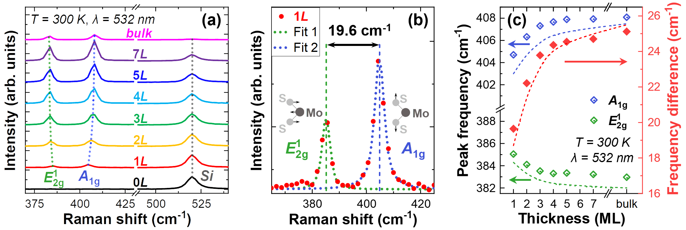
To double-check the layer thickness, Raman spectroscopy measurements were carried out in different regions using a cw 532 nm laser in an air ambient environment (Fig. S7(a)). This method is based on the fact that the Raman frequencies of the mode (in-plane opposite vibrations of S and Mo atoms, illustrated in Fig. S7(b)) and the mode (out-of-plane vibration of S atoms in opposite directions, illustrated in Fig. S7(b)) are highly sensitive to MoS2 thickness within the range of 1-4 MLs 51. Especially, the difference between the two peaks in ML-MoS2 generally falls within the range of 18-21 cm-1, regardless of the laser 53 or substrate 54 used. Therefore, this feature is commonly used to identify ML-MoS2. In our case, the observed thickness-dependent Raman peaks and the frequency difference between the two peaks (diamonds in Fig. S7(c)) align well with the reported trend (dashed curves in Fig. S7(c)) 51, thus corroborating the thickness determined by AFM. Furthermore, the presence of a ML-MoS2 region () in the flakes of interest, which is crucial for our study, is well confirmed (Fig. S7(b)).
9 5. CL data processing
The hyperspectral analysis was conducted using the hyperspy package in Python 55. For each pixel in the hyperspectral map, a multi-peak fitting is employed to extract the integrated intensity of the GaN QW and AlGaN spacer emissions (Figs. S8(a, b)), which enables the generation of integrated intensity maps for each emission within the scanned area (Figs. S8(c, d)).
To extract information from regions with different MoS2 thicknesses, we employed image segmentation on the high-resolution optical micrograph of the flake (Figs. S9(a, b)). This is based on the thickness-sensitive color contrast mentioned earlier. Consequently, regions with different thicknesses are assigned specific colors, \latini.e., defined pixel values. The resulting segmented image was then rotated and resized to align it with the contour of the flake in the panchromatic CL map (Fig. S9(c)). The reshaped image was subsequently cropped and binned to generate a mask for the CL map, ensuring that its image size and number of pixels are the same as the CL map (Fig. S9(d)). Due to the lower resolution of the CL map, pixels located at the boundaries of the segmented regions exhibit intermediate values after the binning process. To address this, all these new pixel values were converted to (255, 255, 255) (white in color), which represent “dead pixels” and are excluded from further data processing and analysis. For all the CL maps in this study, we generated an associated mask where the color of each pixel represents the number of MoS2 MLs at that position.
The use of thickness-related masks is crucial to our study. Firstly, these masks enable the calculation of the average background intensity () in different emission maps, which allows equivalent normalization of the maps and facilitates comparison across different samples. Specifically, the normalized intensity is calculated using , so that the average background intensity is set to 1 for all maps. In this way, the contrast observed in each map represents the relative change in intensity induced by the presence of MoS2, allowing direct comparisons between different maps. Secondly, instead of comparing solely the intensity maps that primarily reflect spatial variations related to the surface morphology of the sample, we also focus on the spectral domain by comparing the average spectra obtained from regions coated with MoS2 of different thicknesses. The advantage of this analysis is twofold. On the one hand, the average spectrum captures the general properties of the interface effect associated with MoS2 thickness and effectively minimizes the impact of microscale fluctuations arising from surface roughness or other factors that are not the main focus of this study. On the other hand, by averaging a large number of spectra, the resulting spectrum has a higher signal-to-noise ratio. This facilitates quantitative analyses, including the peak identification (\latine.g., ZPL and LO phonon replicas of the GaN QW emission) and the calculation of energy-dependent intensity contrasts (see Fig. 5(b) in the main text). Overall, the use of thickness-related masks enables equivalent data normalization, spectral analysis, and quantitative calculations, which improves the interpretability and reliability of our results.
10 6. MoS2 on bulk GaN epilayer
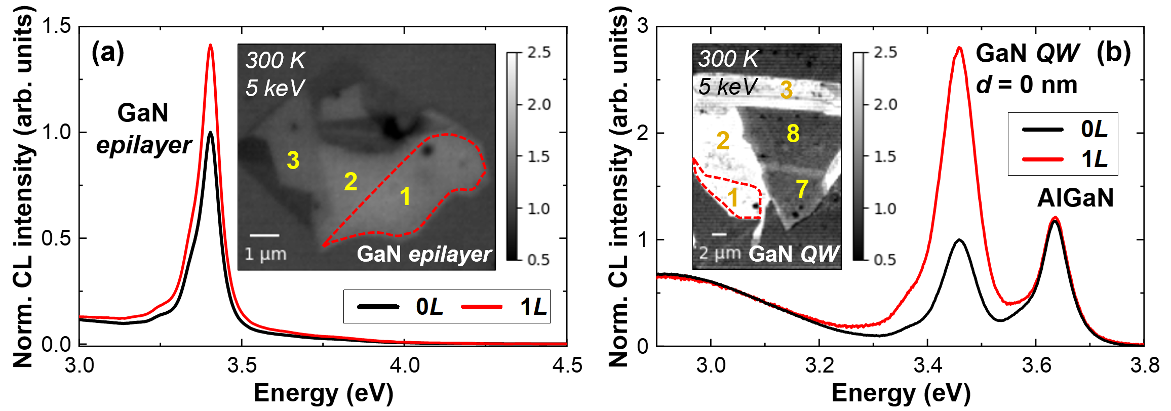
To confirm the hypothesis of the surface passivation effect, we deposited an MoS2 flake of 1-3 MLs on a bulk GaN epilayer, identical to the GaN buffer used to grow the QWs (SI Sec. 1). CL measurement was performed on this flake at 300 K using 5 keV excitation. The resulting GaN intensity map is normalized (inset of Fig. S10(a)) and compared to the normalized GaN QW intensity map of the uncapped GaN QW ( nm) coated with 2D MoS2 (inset of Fig. S10(b)). Through normalization, both maps have the same average background intensity, \latini.e., 1. Upon comparison, it is evident that both maps demonstrate enhanced GaN emission in the presence of MoS2. However, the enhancement is obviously stronger for the uncapped GaN QW emission than for the GaN epilayer emission. To quantitatively visualize this difference, average CL spectra of the bare region () and the region coated with ML-MoS2 () are compared. For the GaN epilayer, the emission is enhanced by ML-MoS2, with a peak intensity ratio of (Fig. S10(a)). In contrast, for the uncapped QW, only the GaN QW emission is enhanced, but with a higher peak intensity ratio of (Fig. S10(b)). This discrepancy in MoS2-induced intensity enhancement between the two cases is consistent with the surface passivation effect. In the uncapped QW, the detected GaN emission comes solely from the surface region, whereas in the GaN epilayer, the emission arises from both surface and bulk regions. As a result, the enhancement is much greater in the former case due to the direct influence of surface passivation.
11 7. MoS2 on GaN QW, nm
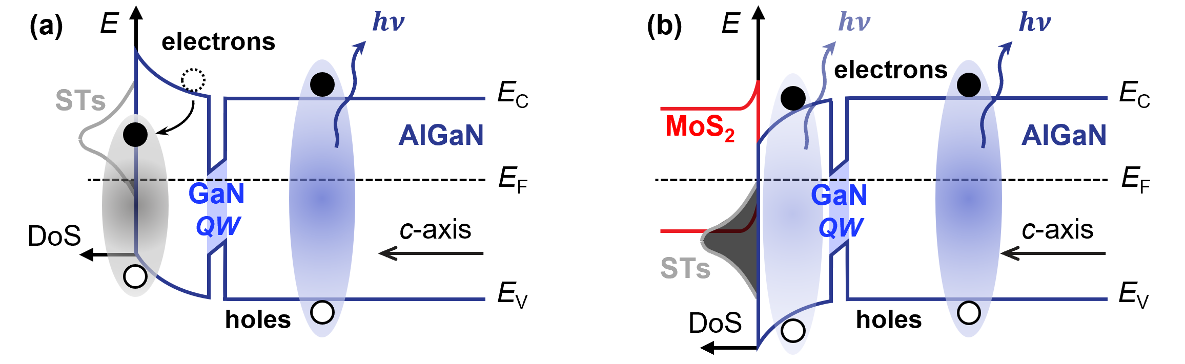
The presence of ML-MoS2 enhances the AlGaN emission from the GaN QW with nm (see Fig. 5(b) in the main text). This enhancement can be attributed to the surface passivation induced by the deposition of ML-MoS2, as illustrated in Fig. S11. In the case of a bare QW without the deposition of MoS2 (Fig. S11(a)), potential emission in the AlGaN surface barrier is quenched due to the presence of STs. Consequently, the AlGaN emission primarily originates from the spacer region, situated far from the surface. Upon the deposition of ML-MoS2 (Fig. S11(b)), the change in surface band bending 12 results in the filling of STs by charges transferred through the vdW interface. As the occupied STs are no longer capable of capturing excitons in the surface region, the emission from the surface AlGaN barrier could potentially be enhanced, which results in an overall increase in the AlGaN emission in the presence of ML-MoS2 coating.
12 8. MoS2 on GaN QWs, nm and nm
Detailed CL results of the QW with nm are presented in Fig. S12. This includes the optical micrograph of the MoS2 flake deposited on a SiO2/Si substrate (Fig. S12(a)), the integrated QW CL intensity map (Fig. S12(b)), and the average CL spectra extracted from the hyperspectral map using the segmentation mask (Fig. S12(c)).
By extracting average spectra from regions with varying MoS2 thicknesses across all the samples in the series, we calculated the CL intensity contrast between the background () and the region coated with ML-MoS2 (), as well as between two other regions with MoS2 thickness differing by 1 ML ( and , with ). As shown in Fig. S13, the contrast observed in other regions, induced by the presence of the additional ML-MoS2 (-to-, light blue curve) aligns with ML-MoS2 spectral absorptance 23 (black dashed curve). However, the contrast observed on the QW surface, resulting from the deposition of a single ML-MoS2 (-to-, blue curve), differs significantly from the absorption behavior and displays distinct peaks associated with the QW emissions. It is worth noting that the shape of these contrast peaks varies between different samples, which is likely due to variations in excitonic transitions within the QWs of different , influenced by structural or material disorders that arise during the growth process. Let us focus on the peak around 3.4 eV (indicated by the red arrow), which corresponds to the ZPL of the QWs. The peak contrast is for nm (Fig. S13(a)), for nm (Fig. S13(b)), and for nm (Fig. S13(c)). The amplitude of this peak reflects the strength of the excitonic interactions between the GaN QW and ML-MoS2. It is evident that the interaction strength is strongly dependent on the distance between the two materials, \latini.e., . This observation is in line with the mechanism of FRET 17.
References
- Nakamura \latinet al. 1994 Nakamura, S.; Mukai, T.; Senoh, M. Candela-class high-brightness InGaN/AlGaN double-heterostructure blue-light-emitting diodes. Appl. Phys. Lett. 1994, 64, 1687–1689
- Steube \latinet al. 1997 Steube, M.; Reimann, K.; Fröhlich, D.; Clarke, S. J. Free excitons with in bulk GaN. Appl. Phys. Lett. 1997, 71, 948–949
- Malpuech \latinet al. 2002 Malpuech, G.; Di Carlo, A.; Kavokin, A.; Baumberg, J. J.; Zamfirescu, M.; Lugli, P. Room-temperature polariton lasers based on GaN microcavities. Appl. Phys. Lett. 2002, 81, 412–414
- Christopoulos \latinet al. 2007 Christopoulos, S.; von Högersthal, G. B. H.; Grundy, A. J. D.; Lagoudakis, P. G.; Kavokin, A. V.; Baumberg, J. J.; Christmann, G.; Butté, R.; Feltin, E.; Carlin, J.-F.; Grandjean, N. Room-temperature polariton lasing in semiconductor microcavities. Phys. Rev. Lett. 2007, 98, 126405
- Novoselov \latinet al. 2004 Novoselov, K. S.; Geim, A. K.; Morozov, S. V.; Jiang, D.; Zhang, Y.; Dubonos, S. V.; Grigorieva, I. V.; Firsov, A. A. Electric field effect in atomically thin carbon films. Science 2004, 306, 666–669
- Chaves \latinet al. 2020 Chaves, A. \latinet al. Bandgap engineering of two-dimensional semiconductor materials. npj 2D Mater. Appl. 2020, 4, 29
- Britnell \latinet al. 2013 Britnell, L.; Ribeiro, R. M.; Eckmann, A.; Jalil, R.; Belle, B. D.; Mishchenko, A.; Kim, Y.-J.; Gorbachev, R. V.; Georgiou, T.; Morozov, S. V.; Grigorenko, A. N.; Geim, A. K.; Casiraghi, C.; Neto, A. H. C.; Novoselov, K. S. Strong light-matter interactions in heterostructures of atomically thin films. Science 2013, 340, 1311–1314
- Mueller and Malic 2018 Mueller, T.; Malic, E. Exciton physics and device application of two-dimensional transition metal dichalcogenide semiconductors. npj 2D Mater. Appl. 2018, 2, 29
- Ciarrocchi \latinet al. 2022 Ciarrocchi, A.; Tagarelli, F.; Avsar, A.; Kis, A. Excitonic devices with van der Waals heterostructures: valleytronics meets twistronics. Nat. Rev. Mater. 2022, 7, 449–464
- Li \latinet al. 2015 Li, D.; Cheng, R.; Zhou, H.; Wang, C.; Yin, A.; Chen, Y.; Weiss, N. O.; Huang, Y.; Duan, X. Electric-field-induced strong enhancement of electroluminescence in multilayer molybdenum disulfide. Nat. Commun. 2015, 6, 7509
- Zhang \latinet al. 2018 Zhang, Z.; Qian, Q.; Li, B.; Chen, K. J. Interface engineering of monolayer MoS2/GaN hybrid heterostructure: modified band alignment for photocatalytic water splitting application by nitridation treatment. ACS Appl. Mater. Interfaces 2018, 10, 17419–17426
- Jain \latinet al. 2020 Jain, S. K.; Kumar, R. R.; Aggarwal, N.; Vashishtha, P.; Goswami, L.; Kuriakose, S.; Pandey, A.; Bhaskaran, M.; Walia, S.; Gupta, G. Current transport and band alignment study of MoS2/GaN and MoS2/AlGaN heterointerfaces for broadband photodetection application. ACS Appl. Electron. Mater. 2020, 2, 710–718
- Chang \latinet al. 1993 Chang, Y.-L.; Tan, I.-H.; Zhang, Y.-H.; Bimberg, D.; Merz, J.; Hu, E. Reduced quantum efficiency of a near-surface quantum well. J. Appl. Phys. 1993, 74, 5144–5148
- Bulashevich and Karpov 2016 Bulashevich, K. A.; Karpov, S. Y. Impact of surface recombination on efficiency of III-nitride light-emitting diodes. Phys. Status Solidi RRL 2016, 10, 480–484
- Grandjean \latinet al. 1999 Grandjean, N.; Damilano, B.; Dalmasso, S.; Leroux, M.; Laügt, M.; Massies, J. Built-in electric-field effects in wurtzite AlGaN/GaN quantum wells. J. Appl. Phys. 1999, 86, 3714–3720
- Bernardini \latinet al. 1997 Bernardini, F.; Fiorentini, V.; Vanderbilt, D. Spontaneous polarization and piezoelectric constants of III-V nitrides. Phys. Rev. B 1997, 56, R10024–R10027
- Förster 1960 Förster, T. Transfer mechanisms of electronic excitation energy. Radiat. Res. Suppl. 1960, 2, 326–339
- Achermann \latinet al. 2004 Achermann, M.; Petruska, M. A.; Kos, S.; Smith, D. L.; Koleske, D. D.; Klimov, V. I. Energy-transfer pumping of semiconductor nanocrystals using an epitaxial quantum well. Nature 2004, 429, 642–646
- Gonzalez \latinet al. 2001 Gonzalez, J. C.; Bunker, K. L.; Russell, P. E. Minority-carrier diffusion length in a GaN-based light-emitting diode. Appl. Phys. Lett. 2001, 79, 1567–1569
- Van de Walle and Segev 2007 Van de Walle, C. G.; Segev, D. Microscopic origins of surface states on nitride surfaces. J. Appl. Phys. 2007, 101, 081704
- Seong and Amano 2020 Seong, T.-Y.; Amano, H. Surface passivation of light emitting diodes: From nano-size to conventional mesa-etched devices. Surf. Interfaces 2020, 21, 100765
- Li \latinet al. 2013 Li, H.; Wu, J.; Huang, X.; Lu, G.; Yang, J.; Lu, X.; Xiong, Q.; Zhang, H. Rapid and reliable thickness identification of two-dimensional nanosheets using optical microscopy. ACS Nano 2013, 7, 10344–10353
- Dumcenco \latinet al. 2015 Dumcenco, D.; Ovchinnikov, D.; Marinov, K.; Lazić, P.; Gibertini, M.; Marzari, N.; Sanchez, O. L.; Kung, Y.-C.; Krasnozhon, D.; Chen, M.-W.; Bertolazzi, S.; Gillet, P.; Fontcuberta i Morral, A.; Radenovic, A.; Kis, A. Large-area epitaxial monolayer MoS2. ACS Nano 2015, 9, 4611–4620
- Castellanos-Gomez \latinet al. 2016 Castellanos-Gomez, A.; Quereda, J.; van der Meulen, H. P.; Agraït, N.; Rubio-Bollinger, G. Spatially resolved optical absorption spectroscopy of single- and few-layer MoS2 by hyperspectral imaging. Nanotechnology 2016, 27, 115705
- Negri \latinet al. 2020 Negri, M.; Francaviglia, L.; Dumcenco, D.; Bosi, M.; Kaplan, D.; Swaminathan, V.; Salviati, G.; Kis, A.; Fabbri, F.; Fontcuberta i Morral, A. Quantitative nanoscale absorption mapping: a novel technique to probe optical absorption of two-dimensional materials. Nano Lett. 2020, 20, 567–576
- Rossbach \latinet al. 2014 Rossbach, G.; Levrat, J.; Jacopin, G.; Shahmohammadi, M.; Carlin, J.-F.; Ganière, J.-D.; Butté, R.; Deveaud, B.; Grandjean, N. High-temperature Mott transition in wide-band-gap semiconductor quantum wells. Phys. Rev. B 2014, 90, 201308
- Shahmohammadi \latinet al. 2014 Shahmohammadi, M.; Jacopin, G.; Rossbach, G.; Levrat, J.; Feltin, E.; Carlin, J.-F.; Ganière, J.-D.; Butté, R.; Grandjean, N.; Deveaud, B. Biexcitonic molecules survive excitons at the Mott transition. Nat. Commun. 2014, 5, 5251
- Klingshirn 2005 Klingshirn, C. F. Semiconductor optics; Springer: Berlin; New York, 2005
- Hofstetter \latinet al. 2020 Hofstetter, D.; Beck, H.; Epler, J. E.; Kirste, L.; Bour, D. P. Evidence of strong electron-phonon interaction in a GaN-based quantum cascade emitter. Superlattices Microstruct. 2020, 145, 106631
- Itskos \latinet al. 2007 Itskos, G.; Heliotis, G.; Lagoudakis, P. G.; Lupton, J.; Barradas, N. P.; Alves, E.; Pereira, S.; Watson, I. M.; Dawson, M. D.; Feldmann, J.; Murray, R.; Bradley, D. D. C. Efficient dipole-dipole coupling of Mott-Wannier and Frenkel excitons in (Ga,In)N quantum well/polyfluorene semiconductor heterostructures. Phys. Rev. B 2007, 76, 035344
- Prins \latinet al. 2014 Prins, F.; Goodman, A. J.; Tisdale, W. A. Reduced dielectric screening and enhanced energy transfer in single- and few-layer MoS2. Nano Lett. 2014, 14, 6087–6091
- Taghipour \latinet al. 2018 Taghipour, N.; Hernandez Martinez, P. L.; Ozden, A.; Olutas, M.; Dede, D.; Gungor, K.; Erdem, O.; Perkgoz, N. K.; Demir, H. V. Near-unity efficiency energy transfer from colloidal semiconductor quantum wells of CdSe/CdS nanoplatelets to a monolayer of MoS2. ACS Nano 2018, 12, 8547–8554
- Feltin \latinet al. 2007 Feltin, E.; Simeonov, D.; Carlin, J.-F.; Butté, R.; Grandjean, N. Narrow UV emission from homogeneous GaN/AlGaN quantum wells. Appl. Phys. Lett. 2007, 90, 021905
- Wang \latinet al. 2013 Wang, L.; Meric, I.; Huang, P. Y.; Gao, Q.; Gao, Y.; Tran, H.; Taniguchi, T.; Watanabe, K.; Campos, L. M.; Muller, D. A.; Guo, J.; Kim, P.; Hone, J.; Shepard, K. L.; Dean, C. R. One-dimensional electrical contact to a two-dimensional material. Science 2013, 342, 614–617
- Castellanos-Gomez \latinet al. 2022 Castellanos-Gomez, A.; Duan, X.; Fei, Z.; Gutierrez, H. R.; Huang, Y.; Huang, X.; Quereda, J.; Qian, Q.; Sutter, E.; Sutter, P. Van der Waals heterostructures. Nat. Rev. Methods Primers 2022, 2, 58
- Drouin \latinet al. 2007 Drouin, D.; Couture, A. R.; Joly, D.; Tastet, X.; Aimez, V.; Gauvin, R. CASINO V2.42 — A fast and easy-to-use modeling tool for scanning electron microscopy and microanalysis users. Scanning 2007, 29, 92–101
- Evoy \latinet al. 1999 Evoy, S.; Harnett, C. K.; Keller, S.; Mishra, U. K.; DenBaars, S. P.; Craighead, H. G. Scanning tunneling microscope-induced luminescence studies of defects in GaN layers and heterostructures. MRS Online Proceedings Library 1999, 588, 19
- Jahn \latinet al. 2022 Jahn, U.; Kaganer, V. M.; Sabelfeld, K. K.; Kireeva, A. E.; Lähnemann, J.; Pfüller, C.; Flissikowski, T.; Chèze, C.; Biermann, K.; Calarco, R.; Brandt, O. Carrier diffusion in : A cathodoluminescence study. I. Temperature-dependent generation volume. Phys. Rev. Appl. 2022, 17, 024017
- Guthrey and Moseley 2020 Guthrey, H.; Moseley, J. A review and perspective on cathodoluminescence analysis of halide perovskites. Adv. Energy Mater. 2020, 10, 1903840
- Brunner \latinet al. 1997 Brunner, D.; Angerer, H.; Bustarret, E.; Freudenberg, F.; Höpler, R.; Dimitrov, R.; Ambacher, O.; Stutzmann, M. Optical constants of epitaxial AlGaN films and their temperature dependence. J. Appl. Phys. 1997, 82, 5090–5096
- Podlipskas \latinet al. 2019 Podlipskas, Z.; Jurkevičius, J.; Kadys, A.; Miasojedovas, S.; Malinauskas, T.; Aleksiejūnas, R. The detrimental effect of AlGaN barrier quality on carrier dynamics in AlGaN/GaN interface. Sci. Rep. 2019, 9, 17346
- Liu 2019 Liu, W. Ultrafast carrier dynamics in III-nitride nanostructures and LED quantum efficiency; Ph.D. Dissertation, École Polytechnique Fédérale de Lausanne, Lausanne, Switzerland, 2019
- Reshchikov \latinet al. 2000 Reshchikov, M. A.; Shahedipour, F.; Korotkov, R. Y.; Wessels, B. W.; Ulmer, M. P. Photoluminescence band near 2.9 eV in undoped GaN epitaxial layers. J. Appl. Phys. 2000, 87, 3351–3354
- Birner \latinet al. 2007 Birner, S.; Zibold, T.; Andlauer, T.; Kubis, T.; Sabathil, M.; Trellakis, A.; Vogl, P. nextnano: General purpose 3-D simulations. IEEE Trans. Electron Devices 2007, 54, 2137–2142
- Rosencher and Vinter 2002 Rosencher, E.; Vinter, B. Optoelectronics; Cambridge University Press: Cambridge, UK, 2002
- Vurgaftman and Meyer 2003 Vurgaftman, I.; Meyer, J. R. Band parameters for nitrogen-containing semiconductors. J. Appl. Phys. 2003, 94, 3675–3696
- Nath \latinet al. 2013 Nath, D. N.; Yang, Z. C.; Lee, C.-Y.; Park, P. S.; Wu, Y.-R.; Rajan, S. Unipolar vertical transport in GaN/AlGaN/GaN heterostructures. Appl. Phys. Lett. 2013, 103, 022102
- Li \latinet al. 2017 Li, C.-K.; Piccardo, M.; Lu, L.-S.; Mayboroda, S.; Martinelli, L.; Peretti, J.; Speck, J. S.; Weisbuch, C.; Filoche, M.; Wu, Y.-R. Localization landscape theory of disorder in semiconductors. III. Application to carrier transport and recombination in light emitting diodes. Phys. Rev. B 2017, 95, 144206
- Triviño \latinet al. 2015 Triviño, N. V.; Butté, R.; Carlin, J.-F.; Grandjean, N. Continuous wave blue lasing in III-nitride nanobeam cavity on silicon. Nano Lett. 2015, 15, 1259–1263
- Benameur \latinet al. 2011 Benameur, M. M.; Radisavljevic, B.; Héron, J. S.; Sahoo, S.; Berger, H.; Kis, A. Visibility of dichalcogenide nanolayers. Nanotechnology 2011, 22, 125706
- Lee \latinet al. 2010 Lee, C.; Yan, H.; Brus, L. E.; Heinz, T. F.; Hone, J.; Ryu, S. Anomalous lattice vibrations of single- and few-layer MoS2. ACS Nano 2010, 4, 2695–2700
- Nemes-Incze \latinet al. 2008 Nemes-Incze, P.; Osváth, Z.; Kamarás, K.; Biró, L. P. Anomalies in thickness measurements of graphene and few layer graphite crystals by tapping mode atomic force microscopy. Carbon 2008, 46, 1435–1442
- Li \latinet al. 2012 Li, H.; Zhang, Q.; Yap, C. C. R.; Tay, B. K.; Edwin, T. H. T.; Olivier, A.; Baillargeat, D. From bulk to monolayer MoS2: Evolution of Raman scattering. Adv. Funct. Mater. 2012, 22, 1385–1390
- Buscema \latinet al. 2014 Buscema, M.; Steele, G. A.; van der Zant, H. S. J.; Castellanos-Gomez, A. The effect of the substrate on the Raman and photoluminescence emission of single-layer MoS2. Nano Res. 2014, 7, 561–571
- de la Peña \latinet al. 2022 de la Peña, F. \latinet al. hyperspy/hyperspy: Release v1.7.3. 2022; https://doi.org/10.5281/zenodo.7263263