Fingerprinting Defects in Hexagonal Boron Nitride via Multi-Phonon Excitation
Abstract
Single photon emitters in hexagonal boron nitride have gathered a lot of attention due to their favourable emission properties and the manifold of possible applications. Despite extensive scientific effort, the exact atomic origin of these emitters has remained unkown thus far. Recently, several studies have tied the emission in the yellow spectral region to carbon-related defects, but the exact atomic structure of the defects remains elusive. In this study, photoluminescence emission and excitation spectroscopy is performed on a large number of emitters within this region. By comparison of the experimental data with theoretical predictions, the origin of yellow single photon emission in hexagonal boron nitride is determined. Knowledge of this atomic structure and its optical properties is crucial for the reliable implementation of these emitters in quantum technologies.
I Introduction
Optical quantum technologies rely on the highly controlled generation of photonic quantum states. A promising way to generate such states in a scalable way are solid-state single photon emitters such as quantum dots or defect centers in diamond [1]. Each of these emitters comes with its specific advantages and disadvantages for usage in quantum technologies and there is an ongoing effort to discover new emitters with more favorable properties.
After the first report in 2016, color centers in hexagonal boron nitride (hBN) have gained increased attention [3]. Being hosted in a layered two-dimensional material, they are fundamentally different from defects in bulk materials such as diamond. Their remarkable optical properties together with their quantum emission at room-temperature make these emitters excellent candidates for technological aplications like integrated photonic structures [4, 5, 6, 7, 8] and quantum cryptography [9, 10]. Defects in hBN exhibit bright and stable emission with high single photon purity at and above room temperature [11] with zero phonon lines (ZPLs) ranging over a broad spectrum from the near-ultraviolet to near-infrared [12, 13, 14, 15, 16, 17]. Certain defects have been shown to possess Fourier-limited linewidth at room temperature [18], tunable internal quantum efficiency [19], spin triplet ground states [20, 21], shelving states [22], as well as a large non-linear excitation cross-section [23]. This hints at a rich underlying level structure of the plethora of possible atomic defects within the large bandgap host material. Understanding the atomic structure of these defects will shed light on their optical levels and the underlying symmetry. If known precisely, a rich level structure is a great resource for quantum technologies. Hence, knowledge of the defects’ atomic structure is of uttermost importance for using such quantum emitters in a scalable way and for the development of novel quantum sensing schemes [21]. A large portion of emitters in hBN investigated so far exhibit ZPL emission in the yellow spectral region around nm ( eV). Recent efforts have connected this emission to carbon-related atomic origins [24, 25, 26, 27, 28, 29]. Optical characteristics can be studied and compared with ab-initio calculations for different carbon defects to further narrow down the exact origin. To this end, photoluminescence excitation (PLE) as well as stimulated emission depletion experiments have been conducted on emitters in the yellow region [30, 31, 32, 33, 25]. Following these previous studies, we perform photoluminescence excitation spectroscopy on a large number of emitters in this spectral region. In our measurements of a large set of emitters, we find a correlation in the excitation characteristics by a value of around meV, which we interpret as a preferred coupling to a single distinct phonon mode. These findings, in combination with ab-initio predicitions, help us to identify the most likely atomic origin out of the carbon-related defects proposed in [34, 31, 35, 36, 27].
II Methods
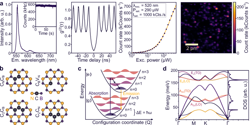
In order to characterize the optical properties of single photon emitters in hBN, we study commercially available hBN nanoflakes on silicon substrate in a homebuilt confocal fluorescence microscope. The samples undergo a consecutive annealing step at °C under a constant nitrogen flow for a duration of one hour. Single emitters are excited by a pulsed ( MHz) supercontinuum source with an accousto optical tunable filter. The excitation laser light is then filtered out and the fluorescence signal from the sample is collected in a single-mode fiber. The emitted light is then either directed to a spectrograph or two avalanche single photon detectors in a Hanbury-Brown-Twiss configuration. For a more detailed description of the setup and sample preparation, the reader is referred to supplementary 1. From confocal scans with an excitation wavelength of nm at a mean excitation power of µW fluorescent spots are selected automatically and characterized (see supplementary 2). The excitation power is chosen due to the typically observed saturation power around this value under pulsed excitation at nm (compare figure 1 a). On the selected spots, we first record photoluminescence excitation spectra by sweeping the excitation wavelength in steps of nm from nm to nm at a fixed power of µW, which is the maximum constant average power our laser system could deliver over this wavelength range. The emission count rate and second-order autocorrelation function are then measured for a duration of s at an excitation wavelength of nm at µW excitation power. From these measurements we analyze the emission stability and confirm the single-photon nature of the emission. Furthermore, we measure the saturation and the photoluminescence (PL) spectrum of the emitter at nm excitation. Exemplary measurements for a selected emitter are shown in figure 1 a.
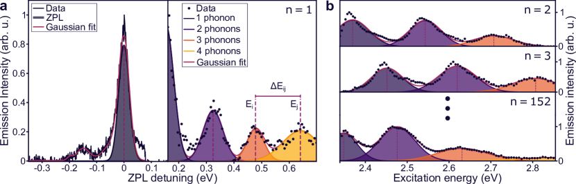
Using this procedure a total of 6143 fluorescent spots have been selected, out of which 3079 showed signs of photobleaching and were discarded during the measurement sequence. The main limiting factor for the further analysis procedure is the blinking behavior of the majority of remaining fluorescent spots. This behavior makes the distinction between significant features of the fluorescent characteristics and temporal instabilities challenging. Thus, only 364 emitters were selected from the remaining 3064 fluorescent spots based on sufficient temporal emission stability as well as single photon purity. The selection criteria are the same for all emitters and are evaluated automatically to avoid any bias in the data (see supplementary 2). On the remaining set of suitable emitters peaks in the recorded PLE spectrum are identified and fitted by a multi-Gaussian function (see supplement 3). In this way information about the transition distribution of individual emitters is retrieved. The recorded PL spectra are analyzed similarly for their zero phonon line and phonon contributions [37, 38] (see supplementary 3). From the fits of the PLE spectra the positions and overall spacing, i.e., energetic distances between distinct transitions of individual emitters are derived. Exemplary evaluation of the measured PLE spectra is shown in figure 2. Consistent spacings between transitions in the PLE spectra can be explained by coupling to a distinct phonon mode in the well-known Huang-Rhys model (see figure 1 c), which phenomenologically describes the interaction between electrons and distinct phonon modes within the surrounding lattice [39, 40]. By comparing these couplings with the theoretically predicted partial Huang-Rhys factors from ab-initio calculations, the atomic origin of the hosted defects can be narrowed down.
III Results
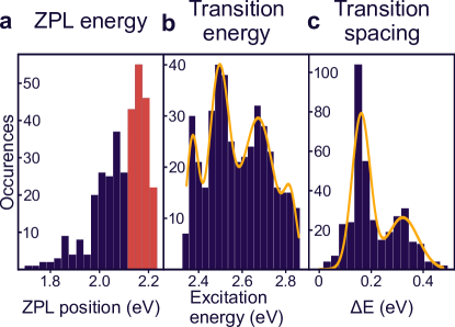
The distribution of measured ZPLs (figure 3 a) shows that the majority of the observed emitters exhibit zero phonon line emission around nm. Further peaks in the ZPL distribution are not significant. As recent studies suggest [24, 34, 26] this predominant yellow emission of single photon emitters in hBN is tied to carbon-related defects. Out of all the different possibilities three distinct candidates, namely , , and (see figure 1 b), show good agreement between ab-initio calculations and experiments [31, 31, 33, 32]. In order to further fingerprint these carbon defects, we restrict the analysis to emitters with ZPL around nm ( eV). This way, a set of 152 emitters remains, as highlighted in figure 3 a. Across all measured transition energies we find four local maxima (fig. 3 b) in the corresponding density. The outer maxima can suffer from errors since we discard peaks in the PLE spectra close to the edge of our experimental range. We therefor focus on the distances between the found transition energies (see fig. 2 a). The density of all extracted energy differences between transitions of individual emitters shows two distinct peaks around meV and meV (fig. 3 c).
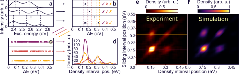
e) Correlations among the measured features in the photoluminescence excitation spectra. The x-axis are the densities of occuring energetic separations on conditional subsets. The center of the slicing interval for building these subsets as described in a) – d) is depicted on the y-axis. f) shows the same evaluation of on a simulated data set with predominant spacing of meV between transitions.
To test if the higher-order maximum can be interpreted as multiple excitations of a single phonon mode, we check whether or not these extracted local maxima are correlated. We do this by performing the previous evaluation on non-disjoint subsets of emitters. These subsets are constructed by chosing a variable energy interval and selecting emitters that exhibit at least one energy difference between their transitions within this interval (fig. 4 a and b). The density of occurring energy differences is then evaluated on each subset (fig. 4 c and d). The evaluation over all subsets is depicted as a heatmap (fig. 4 e), with the centers of the density intervals and the chosen energy intervals given on the x- and y-axis, respectively. The isolated lobes of elavated intensity show that the local maxima at meV and meV are indeed correlated. This characteristic feature is indicative of a phonon-assisted excitation process by coupling to harmonic oscillators of a fixed fundamental energy, as depicted in the Huang-Rhys model. It should be highlighted that since this evaluation concerns differences in the PLE spectra, the second local maxima in the density plot corresponds to at least a threefold excitation of the respective fundamental phonon mode. To determine the contributions of different phonon energies in these results, we simulate the expected behaviour of the PLE data in the presence of well-known discrete phononic contributions. This is done by creating a toy data set that matches the selected spectral region around nm. We focus on three discrete modes located at meV, meV, and meV. The first two values are chosen because of the dominant partial Huang-Rhys factors for these modes for the defects under consideration [36, 27, 34, 31]. The mode at meV is selected heuristically to simulate the visibly increased density around this value (compare figure 3 c). Starting from the ZPL, we distribute further transition lines step by step. The distance from the previous transition is selected from the above mentioned set of phonon energies at fixed relative probabilities. With this approach the PLE data of an emitter can exhibit transitions at fixed energetic spacings or a mixture of phononic modes. By varying the relative probabilities of the different components, we find that a ratio for the respective phonon energies of meV, meV, and meV yields the best agreement with the data. Increasing the content of the latter two modes leads to significant deviations from the experimental data.
IV Discussion
From the measured PLE spectra, we find local maxima in the fluorescence distanced by multiples of meV. From this observation, it is possible to draw conclusions about the atomic origin of these defects via their predicted phonon coupling from first principle calculations. As pointed out in several theoretical studies [34, 31, 35, 36, 27], two likely candidates, the and carbon trimers, show good agreement in terms of the theoretically proposed electron-phonon-coupling (partial Huang-Rhys factors) and experimental results. Out of these two possibilities, the simulated PL and PLE spectra of the center show stronger coupling to phonon modes around meV111The same holds true for the carbon dimer , on which the two trimers are based (see figure 1 d).. In contrast, the trimer shows good agreement with the observed coupling to the phonon mode around meV. In addition, the simulations presented in [31] indicate that higher order phonon sidebands of the defect constitute less resolved traces of the two competing modes, whereas they appear less ambiguous for the center. The observed correlations involving the third order optical phonon mode are thus more likely to stem from the center. Another defect that could potentially match the observed emission around nm, is the carbon-vacancy center. This defect, however, exhibits larger partial Huang-Rhys factors for low-energy phonons [31, 41, 31], making it less likely to be the origin behind the observed emission properties. Our method therefor serves as an identification tool via the exclusion principle. Out of four proposed defects with emission energies in the yellow region, the shows the best agreement with the observed emission characteristics in this study. Another supporting factor for the center as the origin is the additional annealing step in a nitrogen-enriched atmosphere. The higher relative nitrogen concentration during the annealing favors the formation of the over the center due to its lower formation energy according to [27].
Due to the statistical nature of our study, this does not rule out that some emitters may still be related to other defects. In order to put the experimental data into an objective framework it is important to highlight the limitations of this work. Temperature influences the resolution of the PLE spectra via thermal broadening [31, 42, 43]. Similarly mixing of the two competing modes in the higher order phonon excitations could lead to larger errors. These effects, however, will in most cases lead to the identification of the more dominant mode, which favours defect identification via its partial Huang-Rhys factors.
V Conclusion
Across a set of 152 measured emitters in the spectral emission range between meV and meV we found a predominant coupling to the phonon mode of the surrounding lattice. In particular, a large portion of emitters exhibit emission upon excitation via three optical phonons. This observation can be used to connect the exact atomic configuration of the majority of single photon emitters in this range to the carbon trimer (compare figure 1 b) based on theoretical predictions. The identification of the atomic origin of the quantum emission in hBN is a pivotal step toward the implementation of hBN in quantum applications such as quantum computing [44, 45], quantum key distribution [9, 10, 46], or quantum sensing [21, 47, 48]. In order to make emitters in hBN a useful resource, detailed knowledge of its level system is a key requirement. Additionally, the exact identification of the spectral emission and excitation characteristics is paramount for the integration of these emitters into photonic structures. With the study presented here, a decisive step into this direction has been taken. To follow this promising lead further emitters could be chosen even more restrictively. A smaller range of the ZPL position or consideration of the spectral density of the PL spectrum, lifetime, and photon yield could increase the certainty of the defect identification. Furthermore, the experiments presented in [32] could be extended to larger detunings. This way the interaction between the optical dipole and electrical field distortions induced by higher order phonon modes could be taken into account.
VI Acknowledgements
This work was funded by Project Nos. EMPIR 20FUN05 SEQUME and EMPIR 20IND05 QADeT. These projects have received funding from the EMPIR programme co-financed by the Participating States and from the European Union’s 2020 research and innovation programme. This work was also funded by the Deutsche Forschungsgemeinschaft (DFG, German Research Foundation) under Germany’s Excellence Strategy within the Cluster of Excellence QuantumFrontiers (EXC 2123, Project No. 390837967) and within the Cluster of Excellence PhoenixD (EXC 2122, Project No. 390833453).
VII Author declaration
VII.1 Conflicts of interest
The authors have no conflicts of interest to disclose.
VII.2 Author contributions
P. Tieben performed the experiment, evaluated the results, and wrote the manuscript. A. W. Schell designed and supervised the study. All authors discussed and interpreted the data.
VIII Data availability
All raw data used in this study, i.e., all 6143 individual fluorescent spots characterized, are available here: https://doi.org/10.25835/q8oa042o.
References
- Aharonovich et al. [2016] I. Aharonovich, D. Englund, and M. Toth, Solid-state single-photon emitters, Nature Photonics 10, 631 (2016).
- Wang et al. [2016] L. Wang, Y. Pu, A. Soh, Y. Shi, and S. Liu, Layers dependent dielectric properties of two dimensional hexagonal boron nitridenanosheets, AIP Advances 6, 125126 (2016).
- Tran et al. [2016] T. T. Tran, K. Bray, M. J. Ford, M. Toth, and I. Aharonovich, Quantum emission from hexagonal boron nitride monolayers, Nature Nanotechnology 11, 37 (2016).
- Schell et al. [2017a] A. W. Schell, H. Takashima, T. T. Tran, I. Aharonovich, and S. Takeuchi, Coupling quantum emitters in 2d materials with tapered fibers, ACS Photonics 4, 761 (2017a).
- Proscia et al. [2019] N. V. Proscia, R. J. Collison, C. A. Meriles, and V. M. Menon, Coupling of deterministically activated quantum emitters in hexagonal boron nitride to plasmonic surface lattice resonances, Nanophotonics 8, 2057 (2019).
- Karanikolas et al. [2022] V. D. Karanikolas, T. Iwasaki, J. Henzie, N. Ikeda, Y. Yamauchi, Y. Wakayama, T. Kuroda, K. Watanabe, and T. Taniguchi, Plasmon triggered ultrafast operation of color centers in hbn layers (2022).
- Mendelson et al. [2019] N. Mendelson, M. Doherty, M. Toth, I. Aharonovich, and T. Trong Tran, Strain Engineering of Quantum Emitters in Hexagonal Boron Nitride, arXiv e-prints (2019), arXiv:1911.08072 [cond-mat.mtrl-sci] .
- Grosso et al. [2017] G. Grosso, H. Moon, B. Lienhard, S. Ali, D. K. Efetov, M. M. Furchi, P. Jarillo-Herrero, M. J. Ford, I. Aharonovich, and D. Englund, Tunable and high-purity room temperature single-photon emission from atomic defects in hexagonal boron nitride, Nature Communications 8, 705 (2017).
- Samaner et al. [2022] C. Samaner, S. Pacal, G. Mutlu, K. Uyanik, and S. Ates, Free-space quantum key distribution with single photons from defects in hexagonal boron nitride, Advanced Quantum Technologies 5 (2022).
- Al-Juboori et al. [2023] A. Al-Juboori, H. Z. J. Zeng, M. A. P. Nguyen, X. Ai, A. Laucht, A. Solntsev, M. Toth, R. Malaney, and I. Aharonovich, Quantum key distribution using a quantum emitter in hexagonal boron nitride, Advanced Quantum Technologies , 2300038 (2023).
- Kianinia et al. [2017] M. Kianinia, B. Regan, S. A. Tawfik, T. T. Tran, M. J. Ford, I. Aharonovich, and M. Toth, Robust solid-state quantum system operating at 800 k, ACS Photonics 4, 768 (2017).
- Li et al. [2022a] S. Li, A. Pershin, G. Thiering, P. Udvarhelyi, and A. Gali, Ultraviolet quantum emitters in hexagonal boron nitride from carbon clusters, The Journal of Physical Chemistry Letters 13, 3150 (2022a).
- Tan et al. [2019] Q.-H. Tan, J.-M. Lai, X.-L. Liu, Y.-Z. Xue, X.-M. Dou, B.-Q. Sun, W.-B. Gao, P.-H. Tan, and J. Zhang, Robust Ultraviolet to Near-infrared Quantum Emitters in Hexagonal Boron Nitride up to 1100 K (2019) arXiv:1908.06578 [physics.app-ph] .
- Zhigulin et al. [2023] I. Zhigulin, K. Yamamura, V. Ivády, A. Gale, J. Horder, C. J. Lobo, M. Kianinia, M. Toth, and I. Aharonovich, Photophysics of blue quantum emitters in hexagonal boron nitride, Materials for Quantum Technology 3, 015002 (2023).
- Elbadawi et al. [2016] C. Elbadawi, T. Tran, O. Shimoni (nee Kulygin), D. Totonjian, C. Lobo, G. Grosso, H. Moon, D. Englund, M. Ford, I. Aharonovich, and M. Toth, Ultra-bright emission from hexagonal boron nitride defects as a new platform for bio-imaging and bio-labelling (2016) p. 1001314.
- Castelletto et al. [2020] S. Castelletto, F. A. Inam, S. ichiro Sato, and A. Boretti, Hexagonal boron nitride: a review of the emerging material platform for single-photon sources and the spin–photon interface, Beilstein Journal of Nanotechnology 11, 740 (2020).
- Camphausen et al. [2020] R. Camphausen, L. Marini, S. A. Tawfik, T. T. Tran, M. J. Ford, and S. Palomba, Observation of near-infrared sub-poissonian photon emission in hexagonal boron nitride at room temperature, APL Photonics 5, 076103 (2020).
- Hoese et al. [2020] M. Hoese, P. Reddy, A. Dietrich, M. K. Koch, K. G. Fehler, M. W. Doherty, and A. Kubanek, Mechanical decoupling of quantum emitters in hexagonal boron nitride from low-energy phonon modes, Science Advances 6, eaba6038 (2020).
- Schell et al. [2017b] A. Schell, M. Svedendahl, and R. Quidant, Quantum emitters in hexagonal boron nitride have spectrally tunable quantum efficiency, Advanced Materials 30 (2017b).
- Gottscholl et al. [2020] A. Gottscholl, M. Kianinia, V. Soltamov, S. Orlinskii, G. Mamin, C. Bradac, C. Kasper, K. Krambrock, A. Sperlich, M. Toth, I. Aharonovich, and V. Dyakonov, Initialization and read-out of intrinsic spin defects in a van der waals crystal at room temperature, Nature Materials 19, 540 (2020).
- Vaidya et al. [2023] S. Vaidya, X. Gao, S. Dikshit, I. Aharonovich, and T. Li, Quantum sensing and imaging with spin defects in hexagonal boron nitride (2023).
- Kianinia et al. [2018] M. Kianinia, C. Bradac, B. Sontheimer, F. Wang, T. T. Tran, M. Nguyen, S. Kim, Z.-Q. Xu, D. Jin, A. W. Schell, C. J. Lobo, I. Aharonovich, and M. Toth, All-optical control and super-resolution imaging of quantum emitters in layered materials, Nature Communications 9, 874 (2018).
- Schell et al. [2016] A. Schell, T. Tran, H. Takashima, S. Takeuchi, and I. Aharonovich, Non-linear excitation of quantum emitters in hexagonal boron nitride multiplayers, APL Photonics 1 (2016).
- Mendelson et al. [2021] N. Mendelson, D. Chugh, J. R. Reimers, T. S. Cheng, A. Gottscholl, H. Long, C. J. Mellor, A. Zettl, V. Dyakonov, P. H. Beton, S. V. Novikov, C. Jagadish, H. H. Tan, M. J. Ford, M. Toth, C. Bradac, and I. Aharonovich, Identifying carbon as the source of visible single-photon emission from hexagonal boron nitride, Nature Materials 20, 321 (2021).
- Li and Gali [2022] S. Li and A. Gali, Bistable carbon-vacancy defects in h-bn, Frontiers in Quantum Science and Technology 1 (2022).
- Huang et al. [2022] P. Huang, M. Grzeszczyk, K. Vaklinova, K. Watanabe, T. Taniguchi, K. S. Novoselov, and M. Koperski, Carbon and vacancy centers in hexagonal boron nitride, Phys. Rev. B 106, 014107 (2022).
- Li et al. [2022b] K. Li, T. J. Smart, and Y. Ping, Carbon trimer as a 2 ev single-photon emitter candidate in hexagonal boron nitride: A first-principles study, Phys. Rev. Mater. 6, L042201 (2022b).
- Li et al. [2023] S. X. Li, T. Ichihara, H. Park, G. He, D. Kozawa, Y. Wen, V. B. Koman, Y. Zeng, M. Kuehne, Z. Yuan, S. Faucher, J. H. Warner, and M. S. Strano, Prolonged photostability in hexagonal boron nitride quantum emitters, Communications Materials 4, 19 (2023).
- Maciaszek et al. [2022] M. Maciaszek, L. Razinkovas, and A. Alkauskas, Thermodynamics of carbon point defects in hexagonal boron nitride, Phys. Rev. Mater. 6, 014005 (2022).
- Jungwirth and Fuchs [2017] N. R. Jungwirth and G. D. Fuchs, Optical absorption and emission mechanisms of single defects in hexagonal boron nitride, Phys. Rev. Lett. 119, 057401 (2017).
- Fischer et al. [2023] M. Fischer, A. Sajid, J. Iles-Smith, A. Hötger, D. I. Miakota, M. K. Svendsen, C. Kastl, S. Canulescu, S. Xiao, M. Wubs, K. S. Thygesen, A. W. Holleitner, and N. Stenger, Combining experiments on luminescent centres in hexagonal boron nitride with the polaron model and ab initio methods towards the identification of their microscopic origin, Nanoscale 15, 14215 (2023).
- Malein et al. [2021] R. N. E. Malein, P. Khatri, A. J. Ramsay, and I. J. Luxmoore, Stimulated emission depletion spectroscopy of color centers in hexagonal boron nitride, ACS Photonics 8, 1007 (2021).
- Preuss et al. [2022] J. A. Preuss, D. Groll, R. Schmidt, T. Hahn, P. Machnikowski, R. Bratschitsch, T. Kuhn, S. M. de Vasconcellos, and D. Wigger, Resonant and phonon-assisted ultrafast coherent control of a single hbn color center, Optica 9, 522 (2022).
- Jara et al. [2021] C. Jara, T. Rauch, S. Botti, M. A. L. Marques, A. Norambuena, R. Coto, J. E. Castellanos-Águila, J. R. Maze, and F. Munoz, First-principles identification of single photon emitters based on carbon clusters in hexagonal boron nitride, The Journal of Physical Chemistry A 125, 1325 (2021).
- Auburger and Gali [2021] P. Auburger and Á. Gali, Towards ab initio identification of paramagnetic substitutional carbon defects in hexagonal boron nitride acting as quantum bits, Physical Review B (2021).
- Sharman et al. [2022] K. Sharman, O. Golami, S. C. Wein, H. Zadeh-Haghighi, C. G. da Rocha, A. Kubanek, and C. Simon, A first-principles calculation of electron-phonon interactions for the and defects in hexagonal boron nitride (2022).
- Wigger et al. [2019] D. Wigger, R. Schmidt, O. D. Pozo-Zamudio, J. A. Preuß, P. Tonndorf, R. Schneider, P. Steeger, J. Kern, Y. Khodaei, J. Sperling, S. M. de Vasconcellos, R. Bratschitsch, and T. Kuhn, Phonon-assisted emission and absorption of individual color centers in hexagonal boron nitride, 2D Materials 6, 035006 (2019).
- Bommer and Becher [2019] A. Bommer and C. Becher, New insights into nonclassical light emission from defects in multi-layer hexagonal boron nitride, Nanophotonics 8, 2041 (2019).
- Huang et al. [1950] K. Huang, A. Rhys, and N. F. Mott, Theory of light absorption and non-radiative transitions in -centres, Proceedings of the Royal Society of London. Series A. Mathematical and Physical Sciences 204, 406 (1950).
- Zhang [2019] Y. Zhang, Applications of huang–rhys theory in semiconductor optical spectroscopy, Journal of Semiconductors 40, 091102 (2019).
- Tawfik et al. [2017] S. A. Tawfik, S. Ali, M. Fronzi, M. Kianinia, T. T. Tran, C. Stampfl, I. Aharonovich, M. Toth, and M. J. Ford, First-principles investigation of quantum emission from hbn defects, Nanoscale 9, 13575 (2017).
- Jungwirth et al. [2016] N. R. Jungwirth, B. Calderon, Y. Ji, M. G. Spencer, M. E. Flatté, and G. D. Fuchs, Temperature dependence of wavelength selectable zero-phonon emission from single defects in hexagonal boron nitride, Nano Letters 16, 6052 (2016).
- Tan et al. [2022] Q. Tan, J.-M. Lai, X.-L. Liu, D. Guo, Y. Xue, X. Dou, B.-Q. Sun, H.-X. Deng, P.-H. Tan, I. Aharonovich, W. Gao, and J. Zhang, Donor–acceptor pair quantum emitters in hexagonal boron nitride, Nano Letters 22, 1331 (2022).
- Couteau et al. [2023] C. Couteau, S. Barz, T. Durt, T. Gerrits, J. Huwer, R. Prevedel, J. Rarity, A. Shields, and G. Weihs, Applications of single photons to quantum communication and computing, Nature Reviews Physics 5, 326 (2023).
- Fournier et al. [2022] C. Fournier, S. Roux, K. Watanabe, T. Taniguchi, S. Buil, J. Barjon, J.-P. Hermier, and A. Delteil, Two-photon interference from a quantum emitter in hexagonal boron nitride (2022).
- Brańczyk [2017] A. M. Brańczyk, Hong-Ou-Mandel Interference, arXiv e-prints (2017), arXiv:1711.00080 [quant-ph] .
- Degen et al. [2017] C. L. Degen, F. Reinhard, and P. Cappellaro, Quantum sensing, Rev. Mod. Phys. 89, 035002 (2017).
- Lyu et al. [2022] X. Lyu, Q. Tan, L. Wu, C. Zhang, Z. Zhang, Z. Mu, J. Zúñiga-Pérez, H. Cai, and W. Gao, Strain quantum sensing with spin defects in hexagonal boron nitride, Nano Letters 22, 6553 (2022).