Visualizing the Localized Electrons of a Kagome Flat Band
Abstract
Destructive interference between electron wavefunctions on the two-dimensional (2D) kagome lattice induces an electronic flat band, which could host a variety of interesting many-body quantum states. Key to realize these proposals is to demonstrate the real space localization of kagome flat band electrons. In particular, the extent to which the often more complex lattice structure and orbital composition of realistic materials counteract the localizing effect of destructive interference, described by the 2D kagome lattice model, is hitherto unknown. We used scanning tunneling microscopy (STM) to visualize the non-trivial Wannier states of a kagome flat band at the surface of CoSn, a kagome metal. We find that the local density of states associated with the flat bands of CoSn is localized at the center of the kagome lattice, consistent with theoretical expectations for their corresponding Wannier states. Our results show that these states exhibit an extremely small localization length of two to three angstroms concomitant with a strongly renormalized quasiparticle velocity m/s, which is comparable to that of moiré superlattices. Hence, interaction effects in the flat bands of CoSn could be much more significant than previously thought. Our findings provide fundamental insight into the electronic properties of kagome metals and are a key step for future research on emergent many-body states in transition metal based kagome materials.
I I. INTRODUCTION
Electrons occupying flat bands in momentum space are expected to be localized in real space. Hence, materials with electronic flat bands present an attractive venue to explore many-body quantum states that can arise from Coulomb interactions. To date, much interest has been directed to the study of many-body quantum states appearing in moiré flat bands Cao et al. (2018a, b); Serlin et al. (2020); Tang et al. (2020); Regan et al. (2020); Xie et al. (2021). The two-dimensional kagome lattice model, realized through a set of corner sharing triangles (see Fig. 1a), offers an alternative way to realize a topological flat band Sun et al. (2011); Guo and Franz (2009). Here, destructive interference between electron wavefunctions is predicted to result in electronic states with non-trivial real space Wannier functions Kang et al. (2020a) which are localized at atomic length scales. The experimental demonstration of these characteristics will be key toward the realization of various interesting quantum phases, such as zero-field fractional quantum Hall states Tang et al. (2011); Neupert et al. (2011), unconventional superconductivity Cao et al. (2018a), and Hubbard-Mott transitions Tang et al. (2020); Regan et al. (2020). Moreover, a variety of kagome materials that exhibit topological electronic states Ye et al. (2018), superconductivity Ortiz et al. (2020), and chiral charge density waves Arachchige et al. (2022) have been discovered recently. Experimental insights into the electronic properties of kagome metals will generally promote a better understanding of this rich phenomenology.
The kagome metals of the FeSn family have attracted significant interest, because the judicious choice of constituent elements and stoichiometry permits control of the electronic, magnetic, and topological properties Ye et al. (2018); Kang et al. (2020b, a); Liu et al. (2020); Xing et al. (2020); Liu et al. (2018); Sankar et al. (2023). In this regard, CoSn was identified as a particularly promising candidate Sales et al. (2022) in which an advantageous layer stacking sequence combined with the absence of long-range magnetic order results in a set of weakly dispersing bands near Fermi energy () Kang et al. (2020a); Liu et al. (2020); Meier et al. (2020). It is important to appreciate that realistic materials deviate from the 2D kagome lattice model; the electronic coupling in the out-of-plane direction, a more complex lattice structure, and spin-orbit coupling could weaken the electron localization. The inherent interest in flat band systems is in the potential amplification of interaction effects between localized charge carriers. The effective interaction strength is strongly affected by the degree of localization of the relevant orbitals, and how it suffers from these deteriorating effects is not known so far.
Here, we perform the first real-space characterization of electrons occupying a kagome flat band using STM. Such measurements are particularly suited to study the energy-resolved local electronic density of states (LDOS) at atomic resolution and previously helped characterize the flat bands of moiré superlattices Li et al. (2010); Wong et al. (2015); Li et al. (2021). In this work, we use spectroscopic imaging with the STM on the surface of CoSn thin films to visualize the real space localization of kagome flat band electrons. Going beyond a bandwidth characterization in momentum space Kang et al. (2020a); Liu et al. (2020), the high spatial resolution of STM enables us to distinguish the non-trivial Wannier states of the kagome flat band from trivially localized states. Surprisingly, they appear more localized than what earlier theories predict Kang et al. (2020a) and exhibit a strongly renormalized quasiparticle velocity. This suggests the enhancement of interaction effects in these flat bands could be more significant than previously thought.
II II. RESULTS
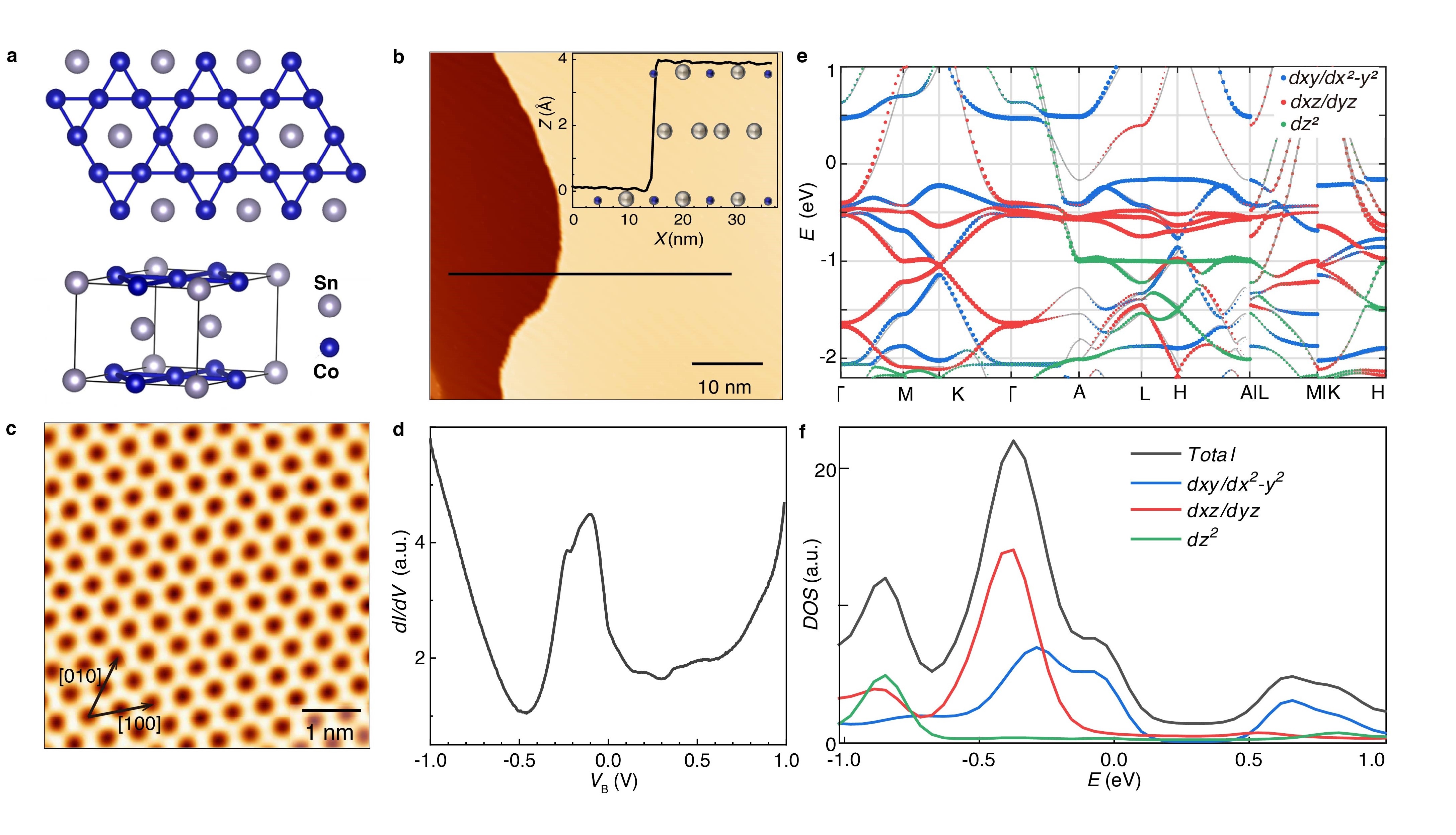
CoSn ( space group, Å, Å) crystallizes in a hexagonal lattice structure that consists of alternating Sn2 honeycomb (stanene) and Co3Sn kagome layers. We prepared CoSn thin films (nominal thickness 50 nm) on the surface of niobium (Nb) doped SrTiO3 (111) by using molecular beam epitaxy (MBE) (see Methods, as well as Ref. SI for materials characterization). The Vollmer-Weber growth mode results in flat top islands with typical diameters of few hundreds of nanometers SI . STM measurements conducted on the surface of these islands show large, atomically flat, and defect-free terraces (Fig. 1b), which makes them suitable for spectroscopic imaging measurements with the STM to visualize the kagome flat bands. High-resolution STM topographies recorded on various islands show that their surface is terminated by a Co3Sn layer, whose apparent height is dominated by the -orbitals of the Co atoms occupying the kagome lattice sites (Fig. 1c) Liu et al. (2020). This observation is consistent with the high substrate temperature °C during film deposition, which disfavors a stanene termination Zhu et al. (2015). A detailed analysis of the Co3Sn lattice structure (Fig. 1a) further reveals the presence of approximately tensile strain along the [010]-direction (crystallographic b-axis), which presumably results from the lattice mismatch () with the substrate.
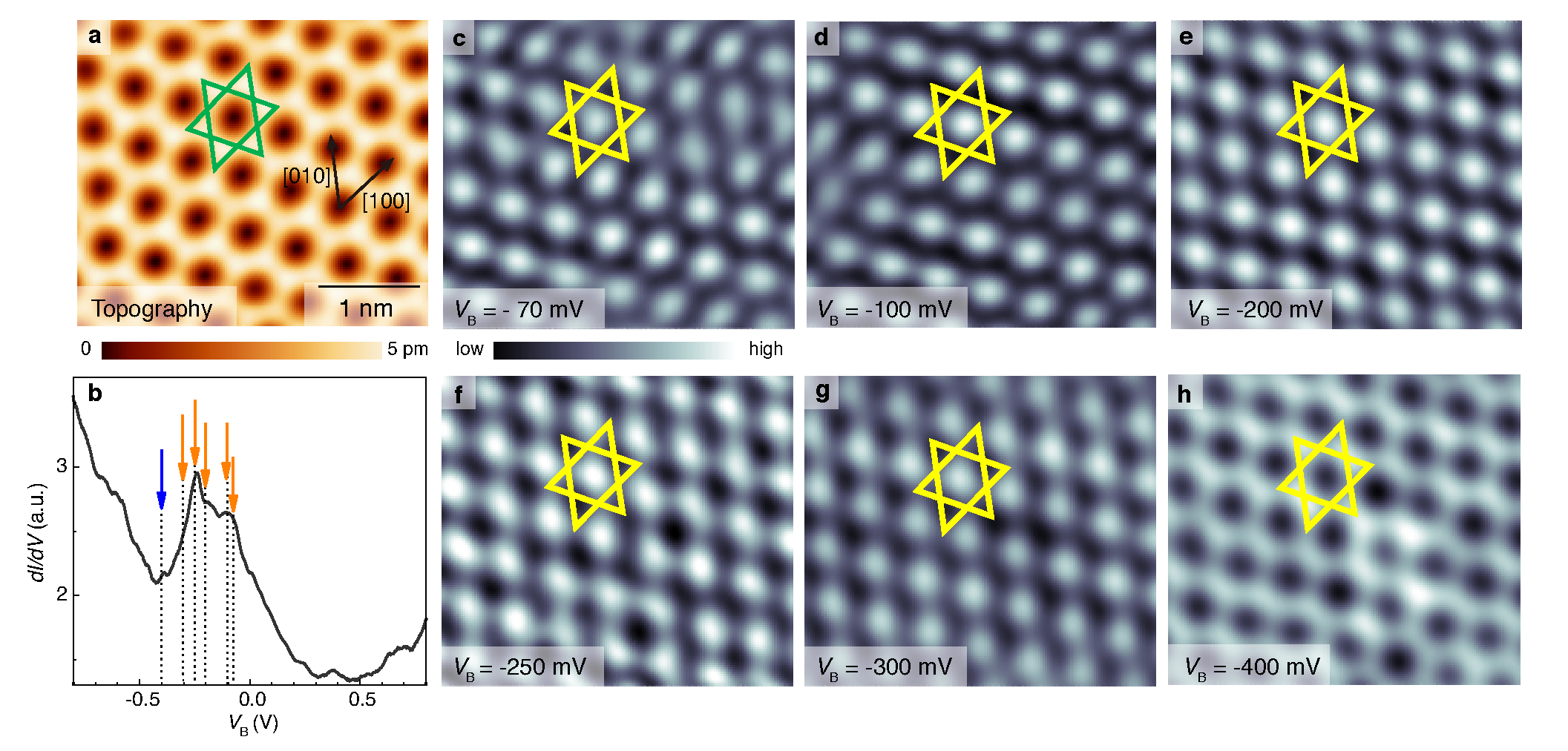
Electronic flat bands manifest as a sharp peak in the differential conductance () spectrum Li et al. (2010); Wong et al. (2015); Xie et al. (2019) of scanning tunneling spectroscopy (STS) measurements, owing to the flat band’s large LDOS () within a small energy window. We have performed STS measurements to detect the presence of such a spectral feature at the surface of CoSn. The spectrum (Fig. 1d) is dominated by a prominent double peak structure, which is located just below zero applied bias voltage . Comparing these characteristics with the electronic structure and LDOS obtained from ab-initio calculations (Fig. 1, d and f, and Methods) and previous results from photo-electron spectroscopy measurements Liu et al. (2020); Kang et al. (2020a), these peaks can be associated with the LDOS of the kagome flat bands. These calculations reveal that two flat bands are situated near Fermi energy and derive from the Co -orbitals (Fig. 1, e and f); The first flat band (FB1), which is located just below , is formed by and orbitals while a second flat band (FB2), appearing at lower energies, originates from the and orbitals. This observation of a pronounced peak associated with the CoSn flat bands contrasts with our results from STM studies on thin films of the iso-structural antiferromagnet FeSn SI . Here, spectra recorded on the Fe3Sn surface lack this distinct feature Lee et al. (2022); Li et al. (2022); Multer et al. (2023), because the electronic structure of FeSn does not have a kagome flat band, owing to the deteriorating influence of strong magnetic exchange terms (see Ref. SI ). We further note that the tensile strain along the [010]-direction slightly modifies the spectral appearance of the peaks associated with the flat band LDOS but it does not significantly affect neither the height nor the width of this spectral feature (see Fig. 2, Fig. 3 and Ref. SI for measurements on other CoSn islands).
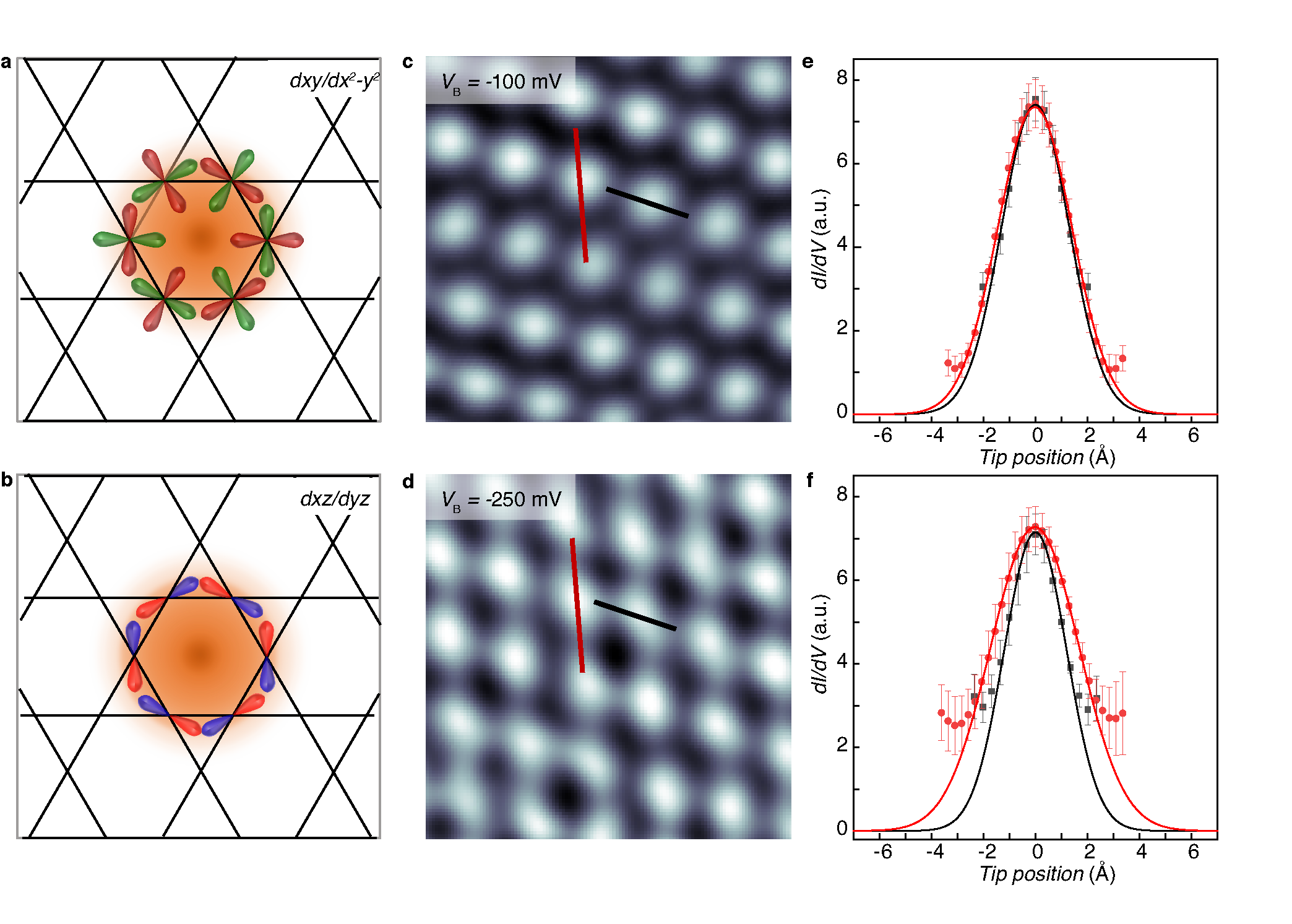
The Wannier functions of -orbital-derived kagome flat bands are expected to be localized at the kagome lattice center Kang et al. (2020a) (cf. Fig. 1a). Our experimental results from spectroscopic imaging measurements are consistent with this expectation (see Ref. SI for results on another CoSn island). The spectroscopic map recorded at a bias voltage = -400 mV (Fig. 2h), which corresponds to an energy outside the flat band peak mirrors the corresponding STM topography (Fig. 2a). It reflects the Co atom positions in the kagome lattice of the Co3Sn layer, whose -orbitals contribute the spectral weight of the dispersive electron bands at this energy (cf. Fig. 1,a and e; denotes the electron charge). Interestingly, spectroscopic maps recorded within the flat band peak at -300 mV mV exhibit a contrast reversal; an enhanced amplitude is observed at the kagome lattice center, which is not occupied by a Co atom (Fig. 2, c to g). We note the Sn atom at the kagome lattice center of the Co3Sn layer (cf. Fig. 1a) contributes negligible spectral weight at these energies and cannot account for the observed characteristics SI . Hence, this observation serves as direct evidence for the non-trivial character of the flat band Wannier states, and it allows us to distinguish them from trivially localized states, which would reside at the kagome lattice sites of the Co atoms. By contrast, the real-space identification of the non-trivial Wannier state of a kagome flat band would not be easily feasible in case of s- and p-orbital derived flat bands, whose spectral weight is expected to reside on the kagome lattice sites Li et al. (2018). Interestingly, the localized LDOS in spectroscopic maps recorded at -100 mV (Fig. 2,c and d) exhibits an circular shaped real space pattern, whereas it appears rather elongated along the [010]-direction in maps recorded at mV and mV (Fig. 2,f and g). This different strain response indicates the different orbital origin of FB1 and FB2, consistent with theoretical expectations (cf. Fig. 1e).
Previous theoretical analyses of the Wannier states of the CoSn flat bands predict a localization length Å Kang et al. (2020a). Interestingly, our quantitative analysis of the spatial distributions reveals much shorter values. We analyze as the spatial decay of the amplitude and apply Gaussian fits to representative line cuts (see Fig. 3, c to f). The -derived FB1 exhibits localization lengths Å and Å along the [100]- and [010]-directions, respectively. Similarly, the -derived FB2 exhibits localization lengths Å and Å along the [100]- and [010]-directions, respectively. While tensile strain along the [010]-direction increases the localization length along this direction, the spectral weight remains predominantly localized at the kagome lattice center (nominal diameter Å).
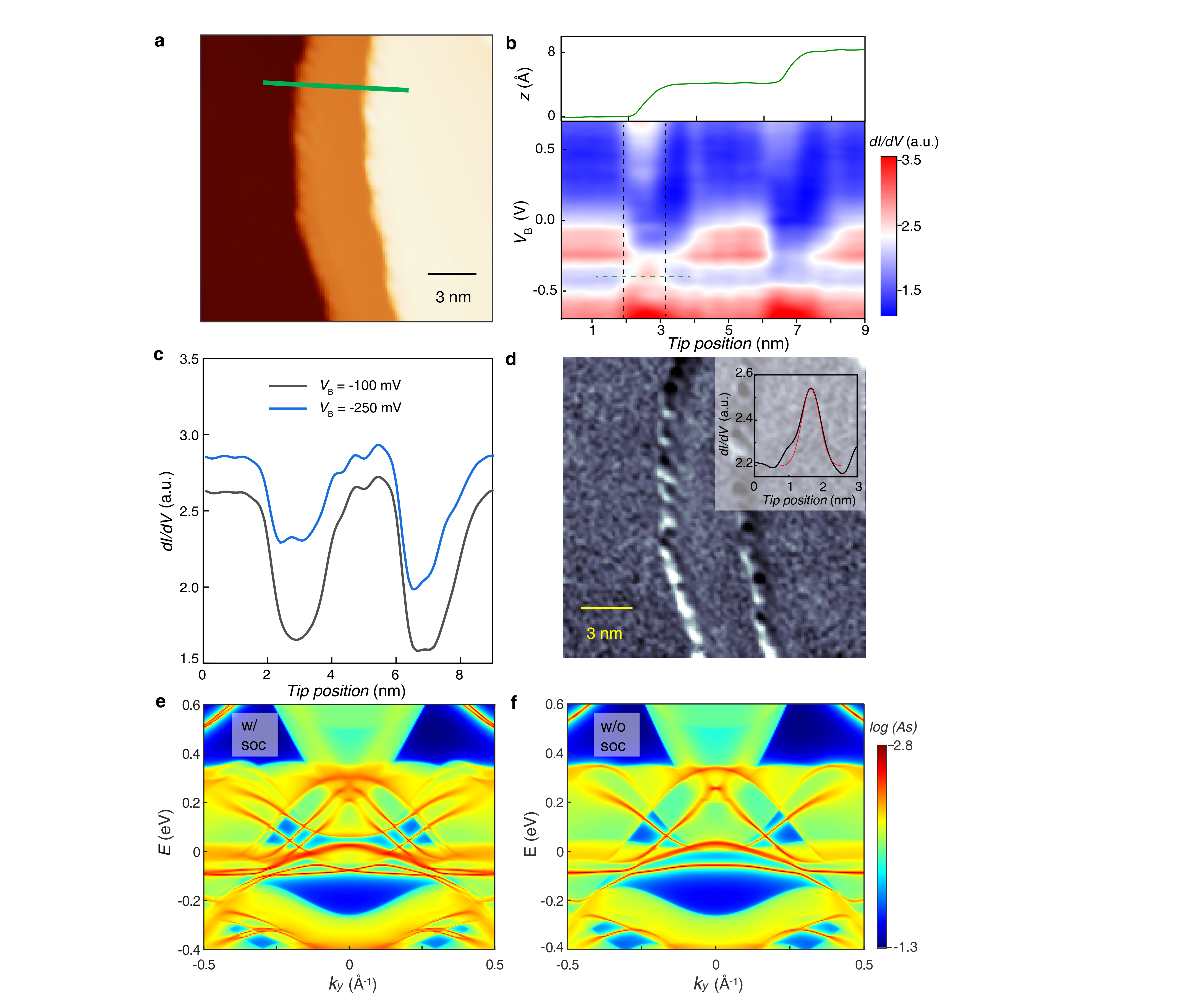
This observed real space localization of the flat band electrons suggests a moderate out-of-plane (crystallographic c-axis) coupling between adjacent Co3Sn layers, that is, the kagome flat band of CoSn should be quasi-two-dimensional. Unlike three-dimensional electronic states which extend into the bulk, 2D electronic states are strongly perturbed by surface defects, such as atoms Heller et al. (1994) and step edges Drozdov et al. (2014). We test the dimensionality of the CoSn flat bands by recording spectra along a line, which crosses two one unit cell high step edges (Fig. 4a). The amplitude associated with the dispersive Co bands at mV weakly responds to the presence of the step edges (Fig. 4b). This is consistent with the observed out-of-plane dispersion of these electronic states in from a previous study Kang et al. (2020a) and indicates their three-dimensional character. By contrast, the flat band amplitude at exhibits a strong response to the presence of step edges and significantly decays over a distance of less than one nanometer (Fig. 4, b and c). This observation indicates the quasi-2D character of the kagome flat bands of CoSn, consistent with a vanishing out-of-plane dispersion of these bands in momentum space Kang et al. (2020a); Liu et al. (2020).
The suppression of the flat band LDOS near atomic step edges permits the presence of a localized edge state in the same energy range (Fig. 4b). Spatial mapping of the amplitude at mV confirms the one-dimensional edge state character of this spectral feature (Fig. 4d) the non-uniform distribution of which suggests that its presence depends on details of the edge termination. Analyzing the characteristic decay length of this state into the quasi-2D bulk, we can estimate the quasiparticle velocity of the kagome flat bands. We extract Å by fitting the spatial decay of the edge state by using a Gaussian function (Fig. 4d inset) and estimate of the kagome flat bands via ( denotes Planck’s constant). Previous measurements of the electronic structure of CoSn detected a spin-orbit coupling (SOC) induced spectral gap meV at the -point between -300 meV and -400 meV Kang et al. (2020a). Using these parameters, we obtain m/s, an extremely small value which is comparable to the quasiparticle velocity found in moiré superlattices (e.g., m/s for magic angle twisted bilayer graphene Cao et al. (2018b). This value is also quantitatively comparable to the theoretical estimate m/s in a simple tight-binding approximation ( - crystal momentum) for a calculated hopping parameter meV between the flat band Wannier states Kang et al. (2020a).
Finally, we comment on the discussed topological character of the CoSn flat band Kang et al. (2020a). Interestingly, a SOC-induced spectral gap at the -point imbues the kagome flat band in the 2D limit with a non-trivial index. Our tight-binding model calculations (see Methods and Ref. SI ) of one CoSn layer (1 unit cell thickness, 40-unit cells width) indeed show the presence of 1D edge states, which appear at the flat band energy. They connect the flat bands with the dispersive conduction and valence bands of the 2D bulk over a large energy range (Fig. 4, e and f). However, these states appear both in case SOC is included and excluded and SOC merely induces a spectral splitting. The opening of a non-trivial meV due to SOC Kang et al. (2020a) (see ref. SI for the bulk spectral functions) could indeed reconnect these edge states with the bulk bands in a non-trivial fashion to accommodate the index. While we cannot resolve these details in our calculations, owing to the coupling of the edge states to the metallic bulk states, it will be interesting to conduct further experiments with magnetic scattering centers Jäck et al. (2020) to clarify the topological origin of the observed edge states.
III III. DISCUSSION AND CONCLUSION
Our experimental results demonstrate the real space localization of electrons occupying a kagome flat band. Spectroscopic mapping with the STM allowed us to directly visualize the corresponding non-trivial Wannier states, which results from destructive electron interference. While interlayer and spin-orbit coupling, and a more complex lattice structure appearing under realistic conditions are generally believed to counteract the localization mechanism of destructive interference described in the 2D kagome lattice model, our observations demonstrate that kagome flat band electrons can retain their localized nature despite these effects. This key result also emphasizes the importance of a suitable layer stacking sequence, such as found in CoSn, and may inform future material design efforts to identify other promising kagome flat band materials Meier et al. (2020).
Our quantitative analyses further show that the flat band Wannier states of CoSn are localized with Å, a value much smaller than theoretically expected Kang et al. (2020a). This strong localization is concomitant with a significantly renormalized m/s. Our findings contrast with moiré superlattice materials where the larger spatial extent (e.g., nm for magic angle twisted bilayer graphene) of the flat band Wannier functions Po et al. (2018) affords a comparably small Coulomb on-site repulsion meV Cao et al. (2018b); Xie et al. (2019). Hence, the enhancement of interaction effects in the flat bands of CoSn due to a large eV Kang et al. (2020a) could be even more pronounced than previously thought Huang et al. (2022).
Together, our observations establish transition-metal based kagome metals as a promising venue to explore the emergence of interacting many-body quantum states in a topological flat band at potentially elevated temperatures Sun et al. (2011); Tang et al. (2011); Guo and Franz (2009). We anticipate that chemical Sales et al. (2021) and modulation doping Cheng et al. (2022), as well as lattice strain Kang et al. (2020a) (see Ref. SI for a discussion of tensile strain observed in our study) offer rich opportunities to realize partial flat band occupations at which these effects are expected to appear.
IV ACKNOWLEDGEMENTS
This work has been primarily supported by an early career grant of the Hong Kong RGC through grant No. 26304221 and the Croucher foundation through grant No. CIA22SC02 awarded to B.J. K.T.L. acknowledges the support of the Ministry of Science and Technology, China, and Hong Kong Research Grant Council through grants Nos. 2020YFA0309600, RFS2021-6S03, C6025-19G, AoE/P-701/20, 16310520, 16310219, and 16307622. H.C.P. acknowledges support from the Hong Kong RGC through grant No. 26308021 and the Croucher Foundation through grant No. CF21SC01. C.C. acknowledges support through a postdoctoral fellowship from the Tin Ka Ping foundation.
C.C., J.Z., and S.S. prepared and characterized the samples. C.C. and J.Z. performed the STM measurements and analyzed the data. R.Y. performed the model calculations. All authors discussed the results and contributed to the manuscript, which was written by C.C. and B.J.
V APPENDIX: Methods
V.1 1. Sample preparation
The experiments were performed in a home-built ultra-high vacuum (UHV) MBE-STM system. CoSn thin films were synthesized on single crystal Nb-doped SrTiO3(111) substrates (CrysTec, mm, 0.05 wt% Nb concentration). Prior to the film synthesis, the substrates were prepared by hydrofluoric acid etching and annealed at 1050 °C in an oxygen atmosphere for one hour to prepare atomically flat and nominally oxygen-vacancy-free surfaces. The prepared substrates were loaded into the MBE chamber and annealed in UHV at 600 °C and 850 °C for 60 min and 5 min, respectively to remove residual moisture and surface adsorbates. CoSn films were deposited by co-evaporating Co and Sn from solid source effusion cells at a background pressure mbar. During the growth, the substrate was kept at a constant temperature ( 830 °C) and enclosed by a cryoshroud nominally held at K. The ratio of beam-equivalent pressures (BEPs) was =1:4.3, where and denote the BEPs of Co and Sn, respectively. The nominal thicknesses of the grown films are nm.
V.2 2. STM measurements
The STM and STS measurements were performed at liquid helium temperature and UHV conditions (mbar) using a chemically etched tungsten STM tip. The tip was prepared on a Cu(111) surface by field emission and controlled indention and calibrated against the Cu(111) Shockley surface state before each set of measurements. spectra were recorded using standard lock-in techniques with a small bias modulation chosen between mV to mV at a frequency Hz. maps were recorded using the multi-pass mode. Here, the topographic height profile is first recorded in constant current mode at a suitable bias voltage. In the next step, the recorded topographic profile is replayed under open feedback conditions and the position-dependent amplitude is recorded at a chosen in a set of multiple passes along the same topographic line. This allows for the acquisition of high-quality maps while avoiding set-points effects.
V.3 3. Model calculations
Density functional theory (DFT) calculations were performed using the Vienna Ab-Initio Simulation Package (VASP) Kresse and Furthmüller (1996a, b). The pseudo-potential is from the projector-augmented wave (PAW) method Blöchl (1994), with the exchange-correlation functional given by the generalized-gradient approximation (GGA) parameterized by Perdew-Berke-Ernzerhof (PBE) Perdew et al. (1996).The plane-wave cut-off energy is set to 300 eV, and a -point mesh of is adopted for the first Brillouin zone sampling. The Wannier tight-binding Hamiltonian of bulk is constructed using the Wannier90 package Mostofi et al. (2014); the -orbitals of the Co atoms and the -orbitals of the Sn atoms are selected as the initial projection basis. Based on this tight-binding model of bulk CoSn, the effective Hamiltonian of the geometry with certain real space truncation can be constructed.
References
- Cao et al. (2018a) Y. Cao, V. Fatemi, S. Fang, K. Watanabe, T. Taniguchi, E. Kaxiras, and P. Jarillo-Herrero, Nature 556, 43 (2018a).
- Cao et al. (2018b) Y. Cao, V. Fatemi, A. Demir, S. Fang, S. L. Tomarken, J. Y. Luo, J. D. Sanchez-Yamagishi, K. Watanabe, T. Taniguchi, E. Kaxiras, et al., Nature 556, 80 (2018b).
- Serlin et al. (2020) M. Serlin, C. Tschirhart, H. Polshyn, Y. Zhang, J. Zhu, K. Watanabe, T. Taniguchi, L. Balents, and A. Young, Science 367, 900 (2020).
- Tang et al. (2020) Y. Tang, L. Li, T. Li, Y. Xu, S. Liu, K. Barmak, K. Watanabe, T. Taniguchi, A. H. MacDonald, J. Shan, et al., Nature 579, 353 (2020).
- Regan et al. (2020) E. C. Regan, D. Wang, C. Jin, M. I. Bakti Utama, B. Gao, X. Wei, S. Zhao, W. Zhao, Z. Zhang, K. Yumigeta, et al., Nature 579, 359 (2020).
- Xie et al. (2021) Y. Xie, A. T. Pierce, J. M. Park, D. E. Parker, E. Khalaf, P. Ledwith, Y. Cao, S. H. Lee, S. Chen, P. R. Forrester, et al., Nature 600, 439 (2021).
- Sun et al. (2011) K. Sun, Z. Gu, H. Katsura, and S. D. Sarma, Physical review letters 106, 236803 (2011).
- Guo and Franz (2009) H.-M. Guo and M. Franz, Physical Review B 80, 113102 (2009).
- Kang et al. (2020a) M. Kang, S. Fang, L. Ye, H. C. Po, J. Denlinger, C. Jozwiak, A. Bostwick, E. Rotenberg, E. Kaxiras, J. G. Checkelsky, et al., Nature communications 11, 4004 (2020a).
- Tang et al. (2011) E. Tang, J.-W. Mei, and X.-G. Wen, Physical review letters 106, 236802 (2011).
- Neupert et al. (2011) T. Neupert, L. Santos, C. Chamon, and C. Mudry, Physical review letters 106, 236804 (2011).
- Ye et al. (2018) L. Ye, M. Kang, J. Liu, F. Von Cube, C. R. Wicker, T. Suzuki, C. Jozwiak, A. Bostwick, E. Rotenberg, D. C. Bell, et al., Nature 555, 638 (2018).
- Ortiz et al. (2020) B. R. Ortiz, S. M. Teicher, Y. Hu, J. L. Zuo, P. M. Sarte, E. C. Schueller, A. M. Abeykoon, M. J. Krogstad, S. Rosenkranz, R. Osborn, et al., Physical Review Letters 125, 247002 (2020).
- Arachchige et al. (2022) H. W. S. Arachchige, W. R. Meier, M. Marshall, T. Matsuoka, R. Xue, M. A. McGuire, R. P. Hermann, H. Cao, and D. Mandrus, Physical Review Letters 129, 216402 (2022).
- Kang et al. (2020b) M. Kang, L. Ye, S. Fang, J.-S. You, A. Levitan, M. Han, J. I. Facio, C. Jozwiak, A. Bostwick, E. Rotenberg, et al., Nature materials 19, 163 (2020b).
- Liu et al. (2020) Z. Liu, M. Li, Q. Wang, G. Wang, C. Wen, K. Jiang, X. Lu, S. Yan, Y. Huang, D. Shen, et al., Nature communications 11, 4002 (2020).
- Xing et al. (2020) Y. Xing, J. Shen, H. Chen, L. Huang, Y. Gao, Q. Zheng, Y.-Y. Zhang, G. Li, B. Hu, G. Qian, et al., Nature communications 11, 5613 (2020).
- Liu et al. (2018) E. Liu, Y. Sun, N. Kumar, L. Muechler, A. Sun, L. Jiao, S.-Y. Yang, D. Liu, A. Liang, Q. Xu, et al., Nature physics 14, 1125 (2018).
- Sankar et al. (2023) S. Sankar, R. Liu, X.-J. Gao, Q.-F. Li, C. Chen, C.-P. Zhang, J. Zheng, Y.-H. Lin, K. Qian, R.-P. Yu, et al., arXiv preprint arXiv:2303.03274 (2023).
- Sales et al. (2022) B. Sales, W. Meier, D. Parker, L. Yin, J. Yan, A. May, S. Calder, A. Aczel, Q. Zhang, H. Li, et al., arXiv preprint arXiv:2201.12421 (2022).
- Meier et al. (2020) W. R. Meier, M.-H. Du, S. Okamoto, N. Mohanta, A. F. May, M. A. McGuire, C. A. Bridges, G. D. Samolyuk, and B. C. Sales, Physical Review B 102, 075148 (2020).
- Li et al. (2010) G. Li, A. Luican, J. Lopes dos Santos, A. Castro Neto, A. Reina, J. Kong, and E. Andrei, Nature physics 6, 109 (2010).
- Wong et al. (2015) D. Wong, Y. Wang, J. Jung, S. Pezzini, A. M. DaSilva, H.-Z. Tsai, H. S. Jung, R. Khajeh, Y. Kim, J. Lee, et al., Physical Review B 92, 155409 (2015).
- Li et al. (2021) H. Li, S. Li, M. H. Naik, J. Xie, X. Li, J. Wang, E. Regan, D. Wang, W. Zhao, S. Zhao, et al., Nature materials 20, 945 (2021).
- (25) “see supplementary information to this manuscript,” .
- Zhu et al. (2015) F.-f. Zhu, W.-j. Chen, Y. Xu, C.-l. Gao, D.-d. Guan, C.-h. Liu, D. Qian, S.-C. Zhang, and J.-f. Jia, Nature materials 14, 1020 (2015).
- Xie et al. (2019) Y. Xie, B. Lian, B. Jäck, X. Liu, C.-L. Chiu, K. Watanabe, T. Taniguchi, B. A. Bernevig, and A. Yazdani, Nature 572, 101 (2019).
- Lee et al. (2022) S.-H. Lee, Y. Kim, B. Cho, J. Park, M.-S. Kim, K. Park, H. Jeon, M. Jung, K. Park, J. Lee, et al., Communications Physics 5, 235 (2022).
- Li et al. (2022) H. Li, H. Zhao, Q. Yin, Q. Wang, Z. Ren, S. Sharma, H. Lei, Z. Wang, and I. Zeljkovic, Scientific Reports 12, 14525 (2022).
- Multer et al. (2023) D. Multer, J.-X. Yin, M. S. Hossain, X. Yang, B. C. Sales, H. Miao, W. R. Meier, Y.-X. Jiang, Y. Xie, P. Dai, et al., Communications Materials 4, 17 (2023).
- Li et al. (2018) Z. Li, J. Zhuang, L. Wang, H. Feng, Q. Gao, X. Xu, W. Hao, X. Wang, C. Zhang, K. Wu, et al., Science advances 4, eaau4511 (2018).
- Heller et al. (1994) E. Heller, M. Crommie, C. Lutz, and D. Eigler, Nature 369, 464 (1994).
- Drozdov et al. (2014) I. K. Drozdov, A. Alexandradinata, S. Jeon, S. Nadj-Perge, H. Ji, R. Cava, B. Andrei Bernevig, and A. Yazdani, Nature Physics 10, 664 (2014).
- Jäck et al. (2020) B. Jäck, Y. Xie, B. Andrei Bernevig, and A. Yazdani, Proceedings of the National Academy of Sciences 117, 16214 (2020).
- Po et al. (2018) H. C. Po, L. Zou, A. Vishwanath, and T. Senthil, Physical Review X 8, 031089 (2018).
- Huang et al. (2022) H. Huang, L. Zheng, Z. Lin, X. Guo, S. Wang, S. Zhang, C. Zhang, Z. Sun, Z. Wang, H. Weng, et al., Physical Review Letters 128, 096601 (2022).
- Sales et al. (2021) B. C. Sales, W. Meier, A. F. May, J. Xing, J.-Q. Yan, S. Gao, Y. Liu, M. Stone, A. Christianson, Q. Zhang, et al., Physical Review Materials 5, 044202 (2021).
- Cheng et al. (2022) S. Cheng, B. Wang, I. Lyalin, N. Bagués, A. J. Bishop, D. W. McComb, and R. K. Kawakami, APL Materials 10, 061112 (2022).
- Kresse and Furthmüller (1996a) G. Kresse and J. Furthmüller, Physical review B 54, 11169 (1996a).
- Kresse and Furthmüller (1996b) G. Kresse and J. Furthmüller, Computational materials science 6, 15 (1996b).
- Blöchl (1994) P. E. Blöchl, Physical review B 50, 17953 (1994).
- Perdew et al. (1996) J. P. Perdew, K. Burke, and M. Ernzerhof, Physical review letters 77, 3865 (1996).
- Mostofi et al. (2014) A. A. Mostofi, J. R. Yates, G. Pizzi, Y.-S. Lee, I. Souza, D. Vanderbilt, and N. Marzari, Computer Physics Communications 185, 2309 (2014).