Electrostatic Steering of Thermal Emission with Active Metasurface Control of Delocalized Modes
Abstract
Abstract We theoretically describe and experimentally demonstrate a graphene-integrated metasurface structure that enables electrically-tunable directional control of thermal emission. This device consists of a dielectric slab that acts as a Fabry-Perot (F-P) resonator supporting long-range delocalized modes bounded on one side by an electrostatically tunable metal-graphene metasurface. By varying the Fermi level of the graphene, the accumulated phase of the F-P mode is shifted, which changes the direction of absorption and emission at a fixed frequency. We directly measure the frequency- and angle-dependent emissivity of the thermal emission from a fabricated device heated to 250∘. Our results show that electrostatic control allows the thermal emission at to be continuously steered over , with a peak emissivity maintained above . We analyze the dynamic behavior of the thermal emission steerer theoretically using a Fano interference model, and use the model to design optimized thermal steerer structures.
The mid infrared (MIR) is an important band for applications ranging from free-space laser communicationsCorrigan et al. (2009) to chemical sensing Haas and Mizaikoff (2016); Rodrigo et al. (2015). An optimal MIR source for these applications would be narrowband, and also offer high speed directional control, such that the beam can be rastered over a range of angles, or have a controllable focal point. Typically, such beam-steering is achieved by reflecting a beam using mechanical devices such as gimbal-mounted mirrorsYoo et al. (2013), optical phased arrays of antennaSun et al. (2013a); Han et al. (2020), or liquid crystal-based devicesFrantz et al. (2018). While each of these techniques have their own set of advantages and disadvantages, one limitation common to them all is that they require an external source of light, such as a quantum cascade laser.
An alternative source of MIR light is one that can be found everywhere, thermal radiation. Any material at a non-zero temperature will emit radiation over a broad range of frequencies which, at moderate temperatures (-), is peaked in the MIR. Though thermal emission is typically viewed as incoherent, isotropic, and broadband, recent advances in nanoengineering have demonstrated that it is possible to engineer the emissivity of a structured material to create narrowbandWang et al. (2018) directionalGreffet et al. (2002) emissions that exhibits coherence. These include metasurfaces composed of non-interacting, localized resonator elements tuned to specific wavelengths, such as metallic nanoantennasLiu et al. (2011) or semiconducting nanostructures that exhibit sharp quasi bound-state-int the continuum resonancesDoiron and Naik (2019); Sun et al. (2021). To achieve coherent directional emission, meanwhile, structures that support long-range delocalized modes can be utilized. These include surface waves that are out-coupled via gratingsGreffet et al. (2002); Tsai et al. (2006); Ghanekar et al. (2022), F-P cavitiesWang et al. (2009), photonic crystalsLee et al. (2005); Celanovic et al. (2005); Battula and Chen (2006), epsilon near zero modesXu et al. (2021) and delocalized modes formed by coupled resonatorsOvervig et al. (2021); Weiss et al. (2022); Nolen et al. (2023). In all of these demonstrated devices, heating is all that is required to produce the desired light as the relevant optical modes are excited thermally, thus providing an elegant source of MIR radiation.
Imparting tunability into such devices - which could allow for dynamic beam control and frequency shifting - requires the integration of materials with variable optical properties. Materials with temperature-dependent phases and/or indices, such as GSTChu et al. (2016); Abdollahramezani et al. (2022); Zhang et al. (2021), VO2Rensberg et al. (2016); Nouman et al. (2018); Kim et al. (2019); Audhkhasi and Povinelli (2021), or SiSun et al. (2013b) have been utilized to create metasurfaces that control the magnitude and phase of scattered light in reflection or transmission geometries, but such materials are unsuitable for thermal emission devices that operate at high, constant temperatures. Alternatively, materials with indices that depend on carrier density, including graphene, III-V quantum wells and indium tin oxide (ITO), can be utilized to bestow electrostatic tunability on metasurfaces, and devices that control phase, frequency, and intensity of reflected light have been demonstratedKim et al. (2018, 2022, 2020); Huang et al. (2016); Sarma et al. (2018); Wu et al. (2019). These materials are also chemically and phase stable at high temperatures, which has enabled them to be integrated within thermal-control metasurfaces to electrostatically tune the intensity and frequency of incandescent light in the mid-IRBrar et al. (2015); Park et al. (2018); Inoue et al. (2014). Unfortunately, such materials also introduce ohmic loss which can, in some geometries, suppresses formation of the long-range delocalized modes that are necessary for coherent, directional thermal emission. As such, dynamic angular tuning of thermal emission is an outstanding problem in the field of thermal metasurfaces.
In this work, we theoretically describe and experimentally demonstrate a thermal emission device that can be tuned electrostatically to control the directionality of thermal emission within a narrow bandwidth. We show experimentally that by using a tunable graphene-integrated metasurface as a boundary for a delocalized F-P cavity mode, the thermal emission from a surface at ( \unitcm-1) can be continuously steered by by changing the carrier density of the graphene sheet. Theoretical calculations, meanwhile, show that an optimized geometry using real materials could achieve of continuous tuning.
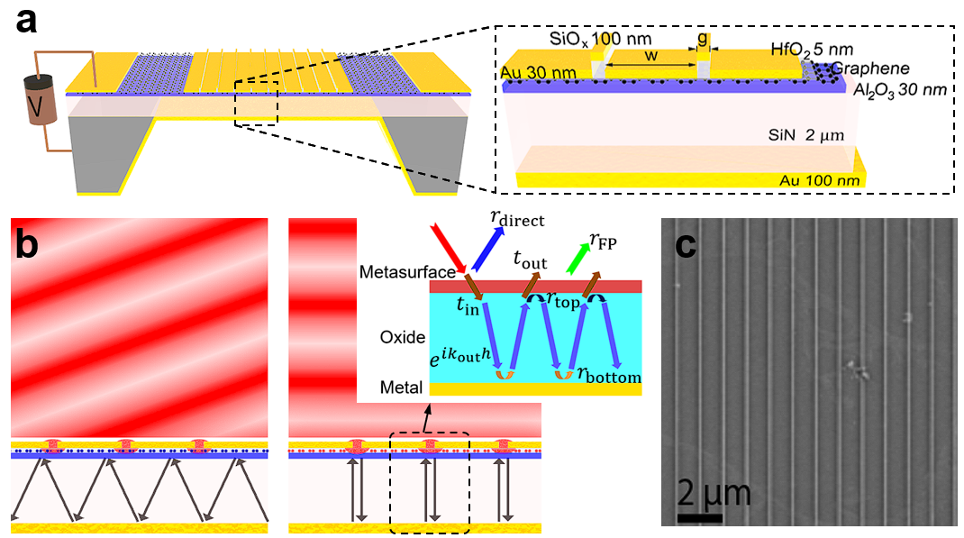
For dynamic thermal emission steering, we utilize an electrically tunable F-P resonance of a SiN dielectric layer sandwiched by a gold back reflector and a graphene-based active metasurface as illustrated in Fig. 1(a). The graphene metasurface consists of thick, wide gold strips spaced 40 nm apart on top of HfO2 (5 nm)/graphene/Al2O3 () trilayer, sitting on the 2 \unit think SiN membrane with the 100 nm gold back reflector that also serves as a back gate electrode. The gaps between the gold strips are filled with a bilayer of gold and 100 nm SiO. The sub-wavelength period of the structure suppresses far-field diffraction except for the zeroth order.
The working principle of our device is illustrated in Fig. 1(b). The graphene-based metasurface covering the top surface of the SiN membrane acts as a partially reflecting mirror to form a vertical F-P cavity. By applying an electrostatic potential () across the dielectric layers, the Fermi level of graphene () is modulated and so are the complex reflection and transmission coefficients of the top graphene metasurface. Consequently, the condition for the resonance shifts, causing a shift in the peak emission angle () for a given frequency. These changes can be qualitatively understood by treating the top metasurface as a two-dimensional sheet with an effective surface admittance, which is justified since the metasurface thickness is about two orders of magnitude shorter than the wavelength of the free space lightJang et al. (2014); Kim et al. (2018); Han et al. (2020). In this model, the subwavelength metallic stips with narrow gaps make the overall optical response of the graphene metasurface to be highly capacitive (i.e. large imaginary impedance) at a low carrier concentration. As the conductivity of graphene raises with increasing , the metasurface exhibits a reduced, but still high, capacitance and also acquires a larger conductance, changing the reflection/transmission characteristics. The quantitative surface admittance model for the graphene metasurface is discussed in detail in Supplementary Notes 1, 2, and 3.
Recognizing the emissivity of a reciprocal object is equal to its absorptivity Kirchhoff (1860), one can understand the mechanism of the directional shift in thermal emission more intuitively by analyzing the absorption process. Since the transmission channel is blocked by the back reflector,
| (1) |
where is the total reflection, which can be decomposed into the direct reflection from the top surface () and the resonant reflection due to the F-P interference formed by multiple reflections inside the dielectric layer (). The interplay between and , both of which are dependent on , determines the overall absorption (and thus the emission) of the device. The absorption peak occurs when and destructively interfere with each other by having similar amplitudes and a phase difference.
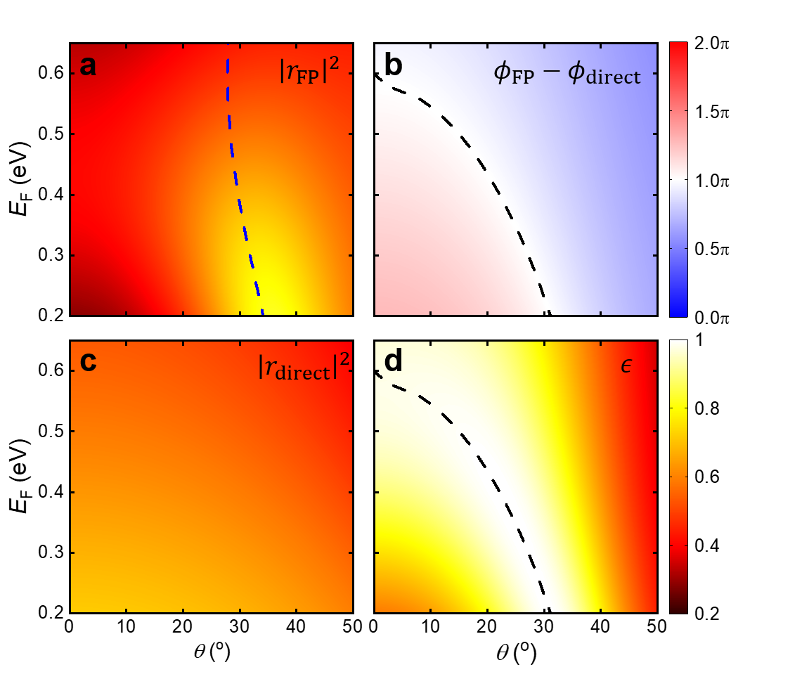
We first theoretically investigate the behavior of the proposed device using full-field electromagnetic simulations based on the finite element method as summarized in Fig. 2. The dependence of on and for TM polarized light is shown in Fig.2(c). can be obtained by simulating the reflection by the graphene metasurface sitting on a semi-infinite SiN layer without a back reflector. Since the top graphene metasurface does not support any distinctive resonance around the target frequency of \unitcm^-1, the direct reflectance, , exhibit a generic weak dependence on within the range of to . As the carrier density of graphene increases, the metasurface becomes less capacitive, leading to better impedance matching as elaborated in (Supplementary Notes 1 and 3). Consequently, monotonically decreases with increasing . The phase of the direct reflection, , remains nearly constant round 0.9 within and .
Unlike , shows a strong dependence on both and due to its resonant nature. The F-P resonance occurs when the out-of-plane wavevector inside the dielectric, , satisfies the constructive interference condition:
| (2) |
where is the phase accumulation associated with vertical wave propagation across the dielectric layer, and are the reflection phase from the top and bottom surfaces, respectively, and is an integer. does not dependent on since the bottom surface is a mere gold back reflector, which behaves like a perfect electric conductor at mid-infrared frequencies. , in principle, could depend on for metasurfaces with an admittance comparable to the surrounding medium, but in our device the admittance is large and, thus, the dependence of is weak for \uniteV. (see Supplementary Note 1 for a detailed analysis). As a result, at a fixed frequency, the resonance angle slightly decreases from to when increases from to as indicated as a blue dashed curve in Fig.2(a); And, at a fixed , the resonance frequency slightly blueshifts with increasing . The F-P resonance becomes weaker with increasing as the top graphene metasurface becomes less reflective and more absorptive, raising both the radiative and dissipative decay rate of the resonant mode. However, while shows only a small dependence on , the overall phase shift due to the F-P resonance () includes phase accumulated while passing into and out of the F-P cavity, through the complex transmission coefficients and , which show considerably more dependence on . (see Supplementary Note 3)
Since the amplitude of is similar to that of near the broad F-P resonance, what mainly determines the overall absorption is their phase difference, . We note that the Fano interference between a non-resonant and) a resonant scattering channel has been widely adopted to create a sharp resonant responseMiroshnichenko et al. (2010); Jang et al. (2018). The dependence of on and , which is dominated by due to the near constant , are plotted in Fig. 2(b). monotonically decreases with because the propagation phase across the dielectric layer, , decreases as shortens. also decreases with as the capacitive phase shift of the top graphene metasurface reduces. As a result, the condition for the Fano resonance, , shifts from to as alters from to . This change in the phase matching condition drives an overall change in the angular-dependent absorptivity/emissivity, shown in Fig.2(d), and thus allows the device to thermally emit at an angle that can be tuned by varying .
In order to experimentally verify the possibility of active thermal emission steering, we fabricated the proposed device using e-beam lithography over a \unitmm^2 area (see Methods), heated it to , and measured its angle-dependent thermal emission spectra while varying the by applying different gate voltages . A polarizer was used to accept only TM polarized emission, and the acceptance angle of the emitted light was . The emissivity of the structure is calculated by normalizing the emitted radiation of the device to the emitted radiation of a reference carbon nanotube blackbodyXiao et al. (2019).
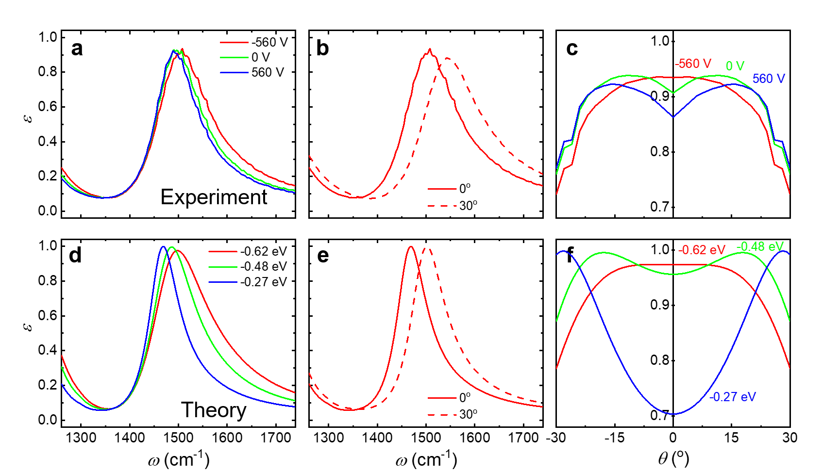
The measured surface normal emissivity spectra for at = 560, 0 and V, shown in Fig.3(a), exhibit a well-defined resonance peak at around \unitcm^-1 that blueshifts as the Fermi level of graphene increases, indicating that the thermal emission peaks are electrostatically tunable with minor variation in the intensity. The measured emissivity spectra also shows a strong angular dependence as shown in Fig.3(b). At a constant doping level ( V), the emission peak shifts from to as changes from to . There are also higher order features present around 2400 \unit^-1 (see Supplementary Note 4) that show similar but more limited shifting. Finally, Fig.3(c) demonstrates the dynamic thermal emission steering by showing how the emission angle is modulated by altering the doping level of graphene at a fixed target frequency \unitcm^-1. At \unitV, we observe that the emission peak is most intense at normal incidence and decreases in intensity as the angle is increased. As the applied gate voltage increases to , the lobe shifts from normal incidence to increasing angles, up to , allowing for continuous tuning in that range.
These experimental results can be compared to simulated emissivity spectra shown in Figures 3(d-f). In these simulations, the value of at \unitV was chosen as a fitting parameter and found to be \uniteV, indicating that the sample is heavily hole-doped, which is consistent with previous studies of graphene grown and transferred using similar proceduresSiegel et al. (2021). Using this initial value of , the Fermi energies at other gate voltages were derived with a simple capacitance model. The overall qualitative behavior of the simulations is consistent with our experimental finding, but the emission lobes are broader and the change of emission angle of the emitter is smaller in our experiment than was theoretically predicted. The likely sources of this inconsistency are the metastructure geometric and material parameter variations across the full 4 x 4 mm2 device (see Subsections A and B in Supplementary Note 5), and carrier density variation during the heating process due to the temperature dependence of the SiN, Al2O3, and HfO2 dielectric propertiesAllers (2004); Bellucci et al. (2021); Bülbül (2007); Chen and Hunter (2004); Dow et al. (2017); Zhu et al. (2002). The estimated carrier density is also affected by substrate and interface charge traps, which can act to decrease the overall doping range (see Methods). We also note that the modulation depth at is predicted to be larger than what is observed experimentally, and we attribute this mostly to decreases in the magnitude of the graphene carrier density due to the filling of charge traps, as well as small potential misalignment of the heating stage. (see Methods) The intensity of emission at large angles can also be reduced due to ellipsoidal elongation of the measurement area which, for small device areas, can extend the active zone to include some low emissivity, unpatterned gold areas.
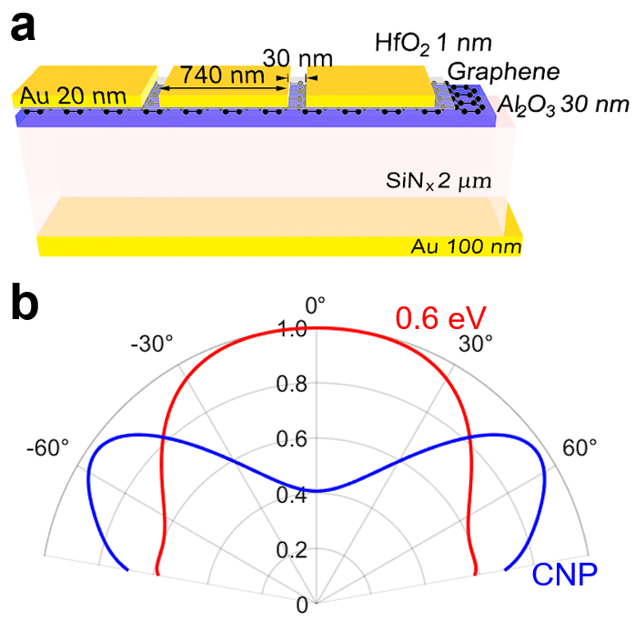
To further explore the potential of the proposed thermal steerer device, we investigate the maximum realizable emission angle under the limitation of realistic geometric and material parameters. The Fermi level of graphene is assumed to be electrostatically tunable between and , considering typical dielectric strength of SiN and numerical optimizations of the geometric parameters of the device were performed to maximize the angle tunability. To prevent performance degradation due to non-local effects (see Supplementary Note 5 for more discussion), we set the minimum gap width to and carried out simulations in the frame of classical electrodynamics. Figure 4(a) shows the structure of the optimized device. The gap and width of Au slit array are and , respectively. The HfO2 is thinned to 1 nm which is achievable smallest value that could avoid quantum tunneling effect. The bilayer Au/SiO area eliminated to enhance interaction between graphene and Au slit array. The optimization results show that it is possible to achieve thermal emission angle steering with unity peak emissivity (Fig.4(b)). The achievable performance is greater than most metasurface-based electrically tunable beam steering devicesBerini (2022) and is comparable to state-of-the-art MEMS-based beam steering device where field of viewZhang et al. (2022). The improvements in the optimized structure in comparison to the experimentally measured sample are due to three main effects. First, the optimized structure utilized a smaller, spacing between the gold strips. This acts to increase the electric field concentration within the graphene and minimize stray fields connecting the gold strips, allowing more interaction with the graphene and a stronger effect of the graphene on the metasurface properties. Second, a thinner HfO2 layer is used in the optimized structure, which brings the graphene closer to the gold and also increases the electric field intensity within the graphene sheet (see Supplementary Notes 2 and 5). And, third, in the optimized structure we assume a greater range of tunability, which is consistent with the potential properties of the dielectrics, but could not be achieved in our experiments due to our methods of contacting the sample (i.e. wirebonding) which weakened the dielectric strength and restricted the range of .
Conclusion
In conclusion, we have demonstrated a thermal emitter that can continuously change the angle of emission in the mid-IR for a designated frequency. We show that by including a graphene-metal metasurface as a boundary, a delocalized F-P optical mode can be tuned to exhibit resonances with angular and frequency dependencies that depend on the carrier density of graphene, which can be tuned electrostatically. The net result is a surface that has an emissivity that is strongly angular dependent and tunable. 16∘ of thermal emission steering at was demonstrated experimentally, and we outline design strategies that could increase the tunability to almost 60∘. This work lays the foundation for next generation beamsteering devices that do not require an external lightsource, and could be broadly applicable for remote sensing and thermal camouflage applications.
Methods
.1 Fabrication of Device
thick, x SiN membranes on a thick Si frame were purchased from Norcada. Metal deposition of the back-reflector consisted of a chromium adhesion layer and of gold. Atomic Layer Deposition (a Fiji G2 ALD) was used to grow a film of Al2O3 on the top of the SiN membrane. Once the Al2O3 was grown, a prepared graphene sheet was transferred on top of the Al2O3 film. Graphene was purchased from Grolltex and was grown on a Cu foil. To remove the foil, first a protective layer of PMMA (950k, A4, MicroChem Corp.) was added on top of the graphene. The Cu foil was etched away with FeCl3 (CE-100, Transene) then the graphene/PMMA stack was rinsed in a series of deionized water baths until transfer to the prepared membranes. Once transferred, the PMMA was removed by soaking in acetone for 1 h. After the graphene transfer, a film of HfO2 was grown via atomic layer deposition. To prepare the SiN membranes for the next steps, the Si frame of the sample was glued to a carrier Si chip with PMMA (950k, A8, MicroChem Corp.). The prepared substrate was then coated with a negative tone hydrogen silesquioxane resist (HSiQ, 6%, DisChem Inc.) at . The sample was then exposed and patterned using the Elionix ELS G-100, an electron beam lithography tool. After exposure, the samples were developed in MF-321 for 90 s, with a 30 s rinse in DI water and then a 30 s rinse in IPA. The development process converts the exposed HSiQ to SiO. For metal deposition of the top, a metal mask was placed above the substrate to create electrically disconnected regions. The deposition consisted of a chromium adhesion layer and of gold. Following these processing steps, the graphene was found to be heavily hole-doped, similar to what has been observed in previous worksSiegel et al. (2021); Brar et al. (2015), Gate-dependent resistivity measurements showed an increase in resistance for positive gate bias, but no maximum resistance was observed that would indicate charge neutrality. These measurements also exhibited hysteresis, consistent with what has been observed elsewhere, and indicative of surface, interface, and substrate charge traps that can be populated with charge as is changed. At high biases, these traps can screen the applied gating field without doping the graphene, leading to deviations from the simple capacitance model that we use to estimate the graphene carrier density for a given Bonmann (2017); Lu et al. (2022); Bartosik et al. (2020).
.2 Thermal Emission Measurements
The emission measurements were performed using a Bruker Vertex 70 FTIR, where thermal emission from a heated sample was used as the lightsource of the interferometer. The device was mounted on a rotation stage, and thermal emission from the device is collected by the aperture in the FTIRXiao et al. (2019). A carbon-nanontube source was used as our blackbody reference measurement. The finite size of the aperture creates a 3∘ acceptance angle, and there is also some uncertainty in the overall angle due to mechanical play in the stage holder and sample tilting within the sample holder. We estimate this uncertainly to be based on measurements with an alignment laser reflected off of an unpatterned area of the sample surface.
.3 Optical Simulations
The frequency-dependent dielectric functions of Al2O3, Cr, Au and SiO were taken from the Palik dataPALIK (1998). The dielectric functions of HfO2 and SiN were obtained from infrared ellipsometryKim et al. (2018). Heat-induced dielectric function change of SiN is corrected through the higher-order F-P resonance peak which is insensitive to Fermi level modulation (see Supplementary Note 4). The graphene was modeled as a layer with zero thickness, and its optical conductivity was calculated by Kubo formula Falkovsky (2008). The carrier mobility of graphene is assumed to be which is comparable to a previously reported value Kim et al. (2018). The reflection/transmission coefficients and absorption spectrum of the proposed structure were calculated by full-wave simulation with the finite element method.
Acknowledgements
J.S. and V.W.B were supported by the Gordon and Betty Moore Foundation through a Moore Inventors Fellowship. M.F. was supported by Office of Naval Research award N00014-20-1-2356. This work was also supported by the National Research Foundation of Korea (NRF) grants funded by the Ministry of Science, ICT and Future Planning (NRF-2022R1A2C2092095, S.K. and M.S.J.) and by the Ministry of Education (NRF-2022R1I1A1A01065727, S.K.).
Author Contributions
These authors contributed equally: Joel Siegel, Shinho Kim.
Conflict of Interests
The authors declare no conflicts of interests.
References
- Corrigan et al. (2009) P. Corrigan, R. Martini, E. A. Whittaker, and C. Bethea, Opt. Express 17, 4355 (2009).
- Haas and Mizaikoff (2016) J. Haas and B. Mizaikoff, Annual Review of Analytical Chemistry 9, 45 (2016).
- Rodrigo et al. (2015) D. Rodrigo, O. Limaj, D. Janner, D. Etezadi, F. J. G. de Abajo, V. Pruneri, and H. Altug, Science 349, 165 (2015).
- Yoo et al. (2013) B.-W. Yoo, M. Megens, T. Chan, T. Sun, W. Yang, C. J. Chang-Hasnain, D. A. Horsley, and M. C. Wu, Opt. Express 21, 12238 (2013).
- Sun et al. (2013a) J. Sun, E. Timurdogan, A. Yaacobi, E. S. Hosseini, and M. R. Watts, Nature 493, 195 (2013a).
- Han et al. (2020) S. Han, S. Kim, S. Kim, T. Low, V. W. Brar, and M. S. Jang, ACS Nano 14, 1166 (2020).
- Frantz et al. (2018) J. A. Frantz, J. D. Myers, R. Y. Bekele, C. M. Spillmann, J. Naciri, J. Kolacz, H. G. Gotjen, V. Q. Nguyen, C. C. McClain, L. B. Shaw, and J. S. Sanghera, J. Opt. Soc. Am. B 35, C29 (2018).
- Wang et al. (2018) Z. Wang, J. K. Clark, Y.-L. Ho, B. Vilquin, H. Daiguji, and J.-J. Delaunay, ACS Photonics 5, 2446 (2018).
- Greffet et al. (2002) J.-J. Greffet, R. Carminati, K. Joulain, J.-P. Mulet, S. Mainguy, and Y. Chen, Nature 416, 61–64 (2002).
- Liu et al. (2011) X. Liu, T. Tyler, T. Starr, A. F. Starr, N. M. Jokerst, and W. J. Padilla, Phys. Rev. Lett. 107, 045901 (2011).
- Doiron and Naik (2019) C. F. Doiron and G. V. Naik, Advanced Materials 31, 1904154 (2019).
- Sun et al. (2021) K. Sun, Z. Zhao, Y. Cai, U. Levy, and Z. Han, Nanophotonics 10, 4035 (2021).
- Tsai et al. (2006) M.-W. Tsai, T.-H. Chuang, C.-Y. Meng, Y.-T. Chang, and S.-C. Lee, Applied physics letters 89 (2006).
- Ghanekar et al. (2022) A. Ghanekar, R. Kapadia, and M. L. Povinelli, Journal of Quantitative Spectroscopy and Radiative Transfer 293, 108367 (2022).
- Wang et al. (2009) L. Wang, B. Lee, X. Wang, and Z. Zhang, International Journal of Heat and Mass Transfer 52, 3024 (2009).
- Lee et al. (2005) B. Lee, C. Fu, and Z. Zhang, Applied Physics Letters 87 (2005).
- Celanovic et al. (2005) I. Celanovic, D. Perreault, and J. Kassakian, Physical Review B 72, 075127 (2005).
- Battula and Chen (2006) A. Battula and S. Chen, Physical Review B 74, 245407 (2006).
- Xu et al. (2021) J. Xu, J. Mandal, and A. P. Raman, Science 372, 393 (2021).
- Overvig et al. (2021) A. C. Overvig, S. A. Mann, and A. Alù, Physical Review X 11, 021050 (2021).
- Weiss et al. (2022) A. Weiss, C. Frydendahl, J. Bar-David, R. Zektzer, E. Edrei, J. Engelberg, N. Mazurski, B. Desiatov, and U. Levy, ACS Photonics 9, 605 (2022).
- Nolen et al. (2023) J. R. Nolen, A. C. Overvig, M. Cotrufo, and A. Alù, arXiv preprint arXiv:2301.12301 (2023).
- Chu et al. (2016) C. H. Chu, M. L. Tseng, J. Chen, P. C. Wu, Y.-H. Chen, H.-C. Wang, T.-Y. Chen, W. T. Hsieh, H. J. Wu, G. Sun, et al., Laser & Photonics Reviews 10, 986 (2016).
- Abdollahramezani et al. (2022) S. Abdollahramezani, O. Hemmatyar, M. Taghinejad, H. Taghinejad, A. Krasnok, A. A. Eftekhar, C. Teichrib, S. Deshmukh, M. A. El-Sayed, E. Pop, et al., Nature communications 13, 1696 (2022).
- Zhang et al. (2021) Y. Zhang, C. Fowler, J. Liang, B. Azhar, M. Y. Shalaginov, S. Deckoff-Jones, S. An, J. B. Chou, C. M. Roberts, V. Liberman, et al., Nature Nanotechnology 16, 661 (2021).
- Rensberg et al. (2016) J. Rensberg, S. Zhang, Y. Zhou, A. S. McLeod, C. Schwarz, M. Goldflam, M. Liu, J. Kerbusch, R. Nawrodt, S. Ramanathan, et al., Nano letters 16, 1050 (2016).
- Nouman et al. (2018) M. T. Nouman, J. H. Hwang, M. Faiyaz, K.-J. Lee, D.-Y. Noh, and J.-H. Jang, Optics express 26, 12922 (2018).
- Kim et al. (2019) Y. Kim, P. C. Wu, R. Sokhoyan, K. Mauser, R. Glaudell, G. Kafaie Shirmanesh, and H. A. Atwater, Nano letters 19, 3961 (2019).
- Audhkhasi and Povinelli (2021) R. Audhkhasi and M. L. Povinelli, Optics Letters 46, 1768 (2021).
- Sun et al. (2013b) J. Sun, E. Timurdogan, A. Yaacobi, E. S. Hosseini, and M. R. Watts, Nature 493, 195 (2013b).
- Kim et al. (2018) S. Kim, M. S. Jang, V. W. Brar, K. W. Mauser, L. Kim, and H. A. Atwater, Nano Letters 18, 971 (2018).
- Kim et al. (2022) J. Y. Kim, J. Park, G. R. Holdman, J. T. Heiden, S. Kim, V. W. Brar, and M. S. Jang, Nature Communications 13, 2103 (2022).
- Kim et al. (2020) S. Kim, S. G. Menabde, V. W. Brar, and M. S. Jang, Advanced Optical Materials 8, 1901194 (2020).
- Huang et al. (2016) Y.-W. Huang, H. W. H. Lee, R. Sokhoyan, R. A. Pala, K. Thyagarajan, S. Han, D. P. Tsai, and H. A. Atwater, Nano letters 16, 5319 (2016).
- Sarma et al. (2018) R. Sarma, S. Campione, M. Goldflam, J. Shank, J. Noh, L. T. Le, M. D. Lange, P. D. Ye, J. Wendt, I. Ruiz, et al., Applied Physics Letters 113 (2018).
- Wu et al. (2019) P. C. Wu, R. A. Pala, G. Kafaie Shirmanesh, W.-H. Cheng, R. Sokhoyan, M. Grajower, M. Z. Alam, D. Lee, and H. A. Atwater, Nature communications 10, 3654 (2019).
- Brar et al. (2015) V. W. Brar, M. C. Sherrott, M. S. Jang, S. Kim, L. Kim, M. Choi, L. A. Sweatlock, and H. A. Atwater, Nat. Commun. 6, 7032 (2015).
- Park et al. (2018) J. Park, J.-H. Kang, X. Liu, S. J. Maddox, K. Tang, P. C. McIntyre, S. R. Bank, and M. L. Brongersma, Science Advances 4, eaat3163 (2018).
- Inoue et al. (2014) T. Inoue, M. D. Zoysa, T. Asano, and S. Noda, Nat. Mater. 13, 928 (2014).
- Jang et al. (2014) M. S. Jang, V. W. Brar, M. C. Sherrott, J. J. Lopez, L. Kim, S. Kim, M. Choi, and H. A. Atwater, Phys. Rev. B 90, 165409 (2014).
- Kirchhoff (1860) G. Kirchhoff, Annalen der Physik 185, 275 (1860).
- Miroshnichenko et al. (2010) A. E. Miroshnichenko, S. Flach, and Y. S. Kivshar, Rev. Mod. Phys. 82, 2257 (2010).
- Jang et al. (2018) M. S. Jang, S. Kim, V. W. Brar, S. G. Menabde, and H. A. Atwater, Phys. Rev. Appl. 10, 054053 (2018).
- Xiao et al. (2019) Y. Xiao, A. Shahsafi, C. Wan, P. J. Roney, G. Joe, Z. Yu, J. Salman, and M. A. Kats, Phys. Rev. Appl. 11, 014026 (2019).
- Siegel et al. (2021) J. F. Siegel, J. H. Dwyer, A. Suresh, N. S. Safron, M. A. Fortman, C. Wan, J. W. Choi, W. Wei, V. Saraswat, W. Behn, M. A. Kats, M. S. Arnold, P. Gopalan, and V. W. Brar, ACS Photonics 8, 1277 (2021).
- Allers (2004) K.-H. Allers, Microelectronics Reliability 44, 411 (2004).
- Bellucci et al. (2021) A. Bellucci, G. Sabbatella, M. Girolami, M. Mastellone, V. Serpente, A. Mezzi, S. Kaciulis, B. Paci, A. Generosi, R. Polini, et al., Energy Technology 9, 2000788 (2021).
- Bülbül (2007) M. Bülbül, Microelectronic engineering 84, 124 (2007).
- Chen and Hunter (2004) L.-Y. Chen and G. W. Hunter, MRS Online Proceedings Library (OPL) 833, G7 (2004).
- Dow et al. (2017) H. S. Dow, W. S. Kim, and J. W. Lee, AIP Advances 7 (2017).
- Zhu et al. (2002) W. Zhu, T.-P. Ma, T. Tamagawa, J. Kim, and Y. Di, IEEE Electron Device Letters 23, 97 (2002).
- Berini (2022) P. Berini, ACS Photonics 9, 2204 (2022).
- Zhang et al. (2022) X. Zhang, K. Kwon, J. Henriksson, J. Luo, and M. C. Wu, Nature 603, 253 (2022).
- Bonmann (2017) M. Bonmann, Effects of impurities on charge transport in graphene field-effect transistors (Chalmers Tekniska Hogskola (Sweden), 2017).
- Lu et al. (2022) Y.-X. Lu, C.-T. Lin, M.-H. Tsai, and K.-C. Lin, Micromachines 13, 509 (2022).
- Bartosik et al. (2020) M. Bartosik, J. Mach, J. Piastek, D. Nezval, M. Konecny, V. Svarc, K. Ensslin, and T. Šikola, ACS sensors 5, 2940 (2020).
- PALIK (1998) E. D. PALIK, Handbook of Optical Constants of Solids, edited by E. D. PALIK (Academic Press, Boston, 1998).
- Falkovsky (2008) L. A. Falkovsky, Journal of Physics: Conference Series 129, 012004 (2008).