Tilt-induced charge localisation in phosphide antiperovskite photovoltaics
Abstract
Antiperovskites are a rich family of compounds with applications in battery cathodes, superconductors, solid-state lighting, and catalysis. Recently, a novel series of antimonide phosphide antiperovskites (\ce3SbP, where = Ca, Sr, Ba) were proposed as candidate photovoltaic absorbers due to their ideal band gaps, small effective masses and strong optical absorption. In this work, we explore this series of compounds in more detail using relativistic hybrid density functional theory. We reveal that the proposed cubic structures are dynamically unstable and instead identify a tilted orthorhombic phase as the ground state. Tilting is shown to induce charge localisation that widens the band gap and increases the effective masses. Despite this, we demonstrate that the predicted maximum photovoltaic efficiencies remain high ( for thin films) by bringing the band gaps into the ideal range for a solar absorber. Finally, we assess the band alignment of the series and suggest hole and electron contact materials for efficient photovoltaic devices.
1 Introduction
Semiconductors with the perovskite \ce3 structure (where and are cations and is an anion) have attracted attention as novel photovoltaics, photodetectors, and light-emitting diodes (LEDs). Reversing the anion and cation sites results in the antiperovskite, or inverse perovskite, \ce3 structure where anions occupy the and sites and cations occupy the sites. Antiperovskites have been widely studied due to their high ionic conductivity,1 giant magnetoresistance,2 superconductivity,3 negative thermal expansion,4 tunable luminescent properties,5 and catalytic performance.6 For this reason, antiperovskites have found use in a broad range of functional applications including superionics for Li and Na ion batteries,7 white LEDs,8 and electrocatalysts.9 There is also considerable interest in antiperovskites as novel photovoltaic materials due to the success of their hybrid perovskite counterparts, which have seen efficiencies rise to in the last decade.10
Although almost half of the elements in the periodic table are stable in the antiperovskite structure11 — satisfying the necessary requirements of ionic radius, electronegativity, and oxidation state — only a handful of compounds with properties suitable for photovoltaics have been observed experimentally. Fabini et al. 12 screened 33,000 known semiconductors from the Inorganic Crystal Structure Database (ICSD) based on their thermodynamic stability, band gap, and optical absorption, and identified over 200 candidates with predicted photovoltaic efficiencies greater than . Among their top predictions were antiperovskite oxides \ce(Ca,Sr)3(Si,Ge)O and nitrides \ce(Ca,Sr,Ba)3(Sb,Bi)N with high predicted efficiencies and light effective masses. Similarly, Kuhar et al. 13 performed a high-throughput search across previously synthesised inorganic compounds and again identified the hexagonal antiperovskite \ceBa3SbN and cubic antiperovskite \ceSr3SbN. Preliminary defect calculations on the compounds suggested that intrinsic vacancies were shallow and that both may possess a degree of defect tolerance. However, the use of a generalised gradient approximation (GGA) density functional, as used in their work, is known to underestimate the depth of defect traps.
A number of studies have computationally screened entire compositional spaces for novel antiperovskite photovoltaics. To date, nitrides have received the most attention, in part due to the preponderance of experimentally known antiperovskite nitride systems (e.g., Heinselman et al. 14 successfully synthesised thin films of \ceMg3SbN revealing favourable visible light absorption). Mochizuki et al. 15 explored the \ce3N space (where = Mg, Ca, Sr, Ba and = P, As, Sb, Bi) through computational elemental substitution in seven crystal structure prototypes. Based on their small effective masses and high optical absorption, they identified \ceMg3PN and \ceSr3PN as novel candidates and further highlighted \ceBa3SbN and \ceSr3SbN as known promising photovoltaics. \ceBa3SbN and \ceSr3SbN were also identified by Kang 16 who explored their optoelectronic properties using GW0, finding band gaps of and , respectively. A follow-up study from the same author investigated the defect physics of \ceBa3SbN using hybrid density functional theory (DFT), which is known to provide increased predictive accuracy compared to semi-local GGA functionals.17 In contrast to previous work,13 they revealed low vacancy and interstitial formation energies that suggests the concentrations of these defects will be high at all accessible synthesis conditions. However, the relatively small charge-capture cross sections of these defects indicates they may not contribute significantly to non-radiative recombination.
A wide range of quaternary antiperovskites have been screened for single-junction and tandem photovoltaic devices. Sreedevi et al. 18 studied the \ce2PN and \ce3P2N2 series (where = Mg, Ca, Sr, Ba, Zn) using hybrid DFT. Despite identifying \ceBa3Sr3P2N2 based on its ideal band gap, its relatively weak optical absorption (only reaching at over ) precludes its use in commercial devices. Similarly, Han et al. 19 screened the series \ce6N2 (where \ce = PAs, PSb, AsSb, PBi, AsBi, SbBi) and \ce62 (where \ce = NP, NAs, PAs, and = Sb, Bi). Their work identified 5 promising antimonides based on their thermodynamic stability, optical absorption, and high dielectric constants (expected to efficiently screen charged impurities). Their most promising candidate, \ceCa6N2AsSb, was investigated in a further study using G0W0+SOC and the Bethe–Salpeter equation (BSE) to confirm its optical performance.20 This work reported an ideal band gap and suggested ideal electron and hole contact materials needed for an efficient photovoltaic device.
Clearly, a wide range of antiperovskite nitrides and antimonides have been studied as potential photovoltaics. However, the phosphide antiperovskites — in which phosphorous is coordinated to two site cations — have received less attention. A recent report from Liang et al. 21 proposed the \ce3SbP series (where = Ca, Sr, Ba) as a novel class of antiperovskite absorbers, with band gaps from and relatively small effective masses. The stability of the series was investigated using elastic constant criteria and the thermodynamic “energy above hull” (found to be in all cases, indicating no competing phases with lower energy). However, this work only reported on the cubic phase of the series, whereas antiperovskites are known to adopt a wide range of structural polytypes, including tilted and other low-dimensional structures. Accordingly, further work is necessary to establish the stability and optoelectronic properties of this class of materials.
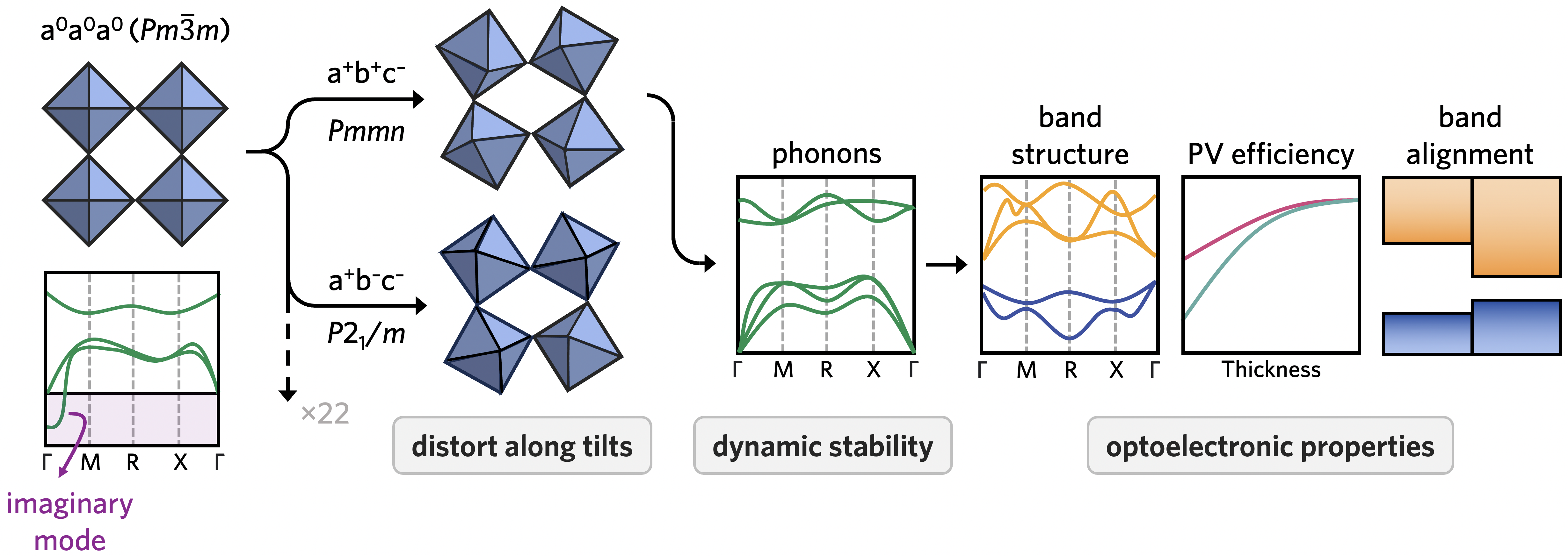
In this work, we use relativistic hybrid density functional theory to investigate the thermodynamic and dynamical stability, optoelectronic properties, and photovoltaic performance of \ce3SbP (where = Ca, Sr, Ba). An overview of the computational approach taken is illustrated in Fig. 1. Vibrational analysis reveals that the cubic phase is dynamically unstable, with imaginary phonon modes indicating spontaneous distortion to lower energy structures. By exploring the 23 tilting patterns possible in the antiperovskite structure, in addition to a number of low-dimensional polytypes, we identify an orthorhombic structure as the ground state in all cases. This tilting is found to induce charge localisation that opens the band gap and slightly reduces the effective masses when compared to the hypothetical cubic structure. Counterintuitively, these effects only marginally impact the predicted photovoltaic efficiency (which is on the order of ), by bringing the band gaps into the ideal range specified by the detailed-balance limit. Finally, we assess the band alignment of the series and suggest hole and electron contact materials for efficient photovoltaic devices.
2 Methodology
All calculations employed Kohn-Sham density functional theory22 using the Vienna Ab initio Simulation Package (VASP).23, 24, 25, 26 The plane-wave energy cutoff and -point mesh were converged to a tolerance of and respectively. All ground state calculations employed an energy cutoff of , with the converged -point meshes presented in Table S1 of the Supplementary Information. Structural optimisations and vibrational properties were performed using the PBEsol exchange–correlation functional27, a version of the PBE functional28 revised for solids. The convergence criteria for energy and forces were set to and , respectively. For accurate descriptions of optoelectronic properties, we employed the Heyd–Scuseria–Ernzerhof hybrid functional (HSE06) for band structures, density of states, and optical absorption calculations.29, 30 The inclusion of spin–orbit coupling (SOC) effects was essential to describe optoelectronic properties accurately due to the presence of heavy Sb atoms. This combination of HSE+SOC has been shown to provide a reliable description of the electronic properties for a range of antimony 31, 32 and bismuth 33 containing materials. Density of states, band structures, and band edge effective masses were obtained using the sumo package.34
The high-frequency dielectric response was calculated using HSE+SOC through the frequency-dependent microscopic polarisability matrix as implemented in VASP.35 The converged -point meshes used to obtain the dielectric response are presented in Table S1 of the Supplementary Information. To analyse the upper radiative limit of thickness-dependent energy conversion, we applied the detailed balance method proposed by Blank et al. 36 — herein termed the “Blank” approach. Band alignment calculations employed a slab structure constructed via the surfaxe package37 with a slab and vacuum thickness of each. A (100) surface was employed, due to its lack of surface dipole and low surface energy.
Vibrational properties were calculated within the harmonic approximation using the finite displacement method as implemented in the phonopy package.38 Vibrational eigenvalues were found to be converged using and supercells for the cubic and orthorhombic structures, respectively. Phonon calculations were performed using the PBEsol functional, with the structure relaxed to a tighter force convergence criterion of . Finite displacements were performed with a energy cutoff, with the converged -point meshes presented in Table S1 of the Supplementary Information.
3 Results and discussion
3.1 Thermodynamic and dynamical stability
Liang et al. 21 proposed that \ce3SbP ( = Ca, Sr, Ba) adopt the cubic antiperovskite structure containing edge sharing \ceP6 octahedra with Sb in the 12-fold cuboctahedral environment. In the cubic structure, all octahedra are aligned with no tilting present, resulting in a 5-atom primitive cell (Fig. 2a). The structural stability of antiperovskites can be predicted using the Goldschmidt tolerance factor,39 , as
| (1) |
where , , and correspond to the radii of the , , and ions of the \ce3 structure. A tolerance factor greater than 1 indicates a hexagonal or tetragonal perovskite structure is most likely to form, a value between indicates a cubic perovskite, between an orthorhombic or rhombohedral perovskite, and a value less than 0.71 is an indicator that alternative non-perovskite structures will be more stable. We calculate tolerance factors between for the \ce3SbP series, strongly indicating that a cubic structure is unlikely. This contrasts with tolerance factors of for the nitride antiperovskites \ce3SbN (where = Ca, Sr, Ba), which are known to crystallise in the cubic (Ca, Sr) and hexagonal (Ba) perovskite structures.15 We note, typically Goldschmidt tolerance factors are calculated using Shannon’s ionic radii, however, the radii for anionic pnictogens \ceP^3- and \ceSb^3- were not reported. Instead, we use the values derived by Mochizuki et al. 15 — namely P () and Sb () — with the remaining values taken from Shannon’s tabulation as Ca (), Sr (), and Ba ().40
The instability of the cubic antiperovskite structures is further highlighted through vibrational analysis. The cubic structures of \ce3SbP were relaxed using the PBEsol exchange–correlation functional and the phonons calculated using the finite-displacement approach implemented in phonopy. The phonon band structures reveal all materials are dynamically unstable with multiple imaginary modes appearing at the -point and persisting across the Brillouin zone. The phonon band structure of cubic \ceBa3SbP is illustrated in Fig. 2c as a representative example. Accordingly, the proposed cubic structures are not a reliable description of the geometry of these compounds, and therefore should not be used to evaluate their photovoltaic performance.
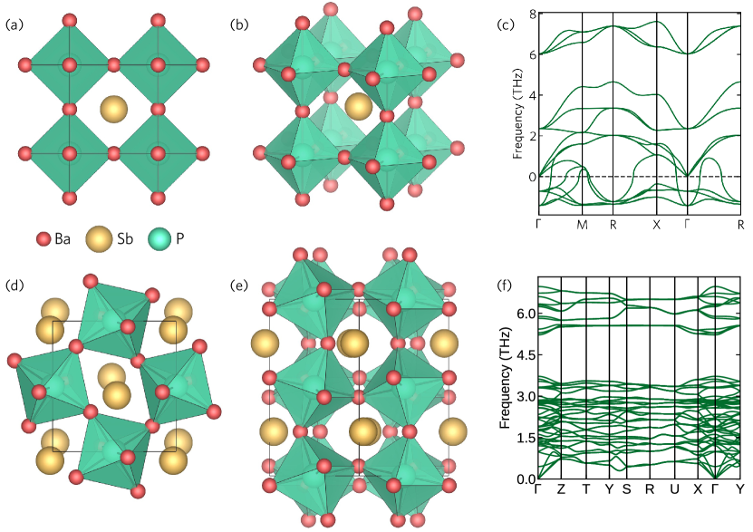
One route to resolving the ground state structure of dynamically unstable phases is through phonon mode-mapping. In this approach, the structure is displaced along the eigenvectors of an imaginary mode and allowed to relaxed. The phonons are recalculated and the process repeated until no imaginary modes remain. This approach has been successfully applied to discover the complex ground state of bismuth stannate containing 176 atoms.41 In contrast, the distortion modes of perovskites were well characterised by Glazer in the 1970s, with only 22 tilting patterns commensurate with the perovskite structure. These tilting patterns can be expressed in Glazer notation as axbycz, where a, b, and c represent the unit cell parameters (if two parameters are the same they share the same letter), while , , denote the rotation of octahedra along that axis and can take values of 0, , and , indicating no-tilt, anti-phase tilt, and in-phase tilt, respectively. Accordingly, for perovskite structures, it is often more computationally efficient to distort along each of the 22 modes directly, as it avoids the need for repeated phonon calculations.
For each member of the \ce3SbP series, we distort the structure along each of the 22 Glazer tilting patterns, with octahedral rotation angles of , , and along the a, b, and c axes. The tilted structures were relaxed using PBEsol and the symmetry of the resulting structure was calculated. In many cases, the structures relaxed away from their initial distortions, resulting in only 11 symmetry inequivalent tilting patterns. We also tested a number of perovskite-like polytypes including the \ceYMnO3 (), ilmenite (), rhombohedral perovskite (), and hexagonal perovskite () structures which cannot be obtained through simple rotations of the antiperovskite structure. The full results are presented in Sections S2 and S3 of the Supplementary Information.
We find that an orthorhombic perovskite structure (space group with a+a-a- tilting) is the ground state for all members of the \ce3SbP series. In each case, the structure is considerably lower in energy than the cubic phase, with the distortion resulting in an energy stabilisation of (Ca), (Sr), and (Ba). This structure is one of the most commonly observed in antiperovskite materials, such as in \ceNa3OCl42 and \ceLi3OCl43. The structure is lower in energy than the next most stable phase ( with a+b+b- tilting for all compositions) by (Ca), (Sr), and (Ba). We note, for Ba this difference is of the order at () and thus the structure may be thermally accessible at room temperature. The dynamic stability of the orthorhombic phase is confirmed by the phonon band structures which reveal the absence of any imaginary modes, as presented in Fig. 2f for \ceBa3SbP. Accordingly, we continue with the ground state orthorhombic structure for the remainder of this work.
As expected, the lattice parameters of the structures are found to increase in line with the ionic radii of the group 2 elements, with an average increase in lattice parameter of for Sr and for Ba relative to \ceCa3SbP. We also find the degree of tilting away from the perfectly cubic structure increases down the group, with the average tilt angles increasing from (Ca) to (Sr) and (Ba). The increase in tilting is in line with the Goldschmidt tolerance factors of the series, which decrease from Ca to Ba (an indication of greater distortion) as detailed above. An additional element of distortion in the antiperovskite structure is the displacement of the Sb ions (which sit in the voids between octahedra) away from their idealised positions. We find the displacement distance also increases down the group, from (Ca) to (Sr) and (Ba). In Table S6 of the Supplementary Materials, we provide the full set of lattice parameters and tilt angles for the series.
3.2 Electronic properties
The band gaps of \ce3SbP calculated using HSE+SOC are presented in Table 1. The band gaps decrease down the group from (Ca) to (Sr) an (Ba). All band gaps are within the ideal range specified by the detailed balance limit ( for a maximum efficiency ). The fundamental band gaps are all direct and appear at the -point in the Brillouin zone as indicated by the band structure of \ceBa3SbP displayed in Fig. 3a. The band structures for Ca and Sr are presented in Fig. S2 of the Supplementary Information. We note that the band gaps are noticeably larger than those of the corresponding antiperovskite nitrides \ceSr3SbN () and \ceBa3SbN ()16, in part due to the greater octahedral tilting present in the phosphide systems.
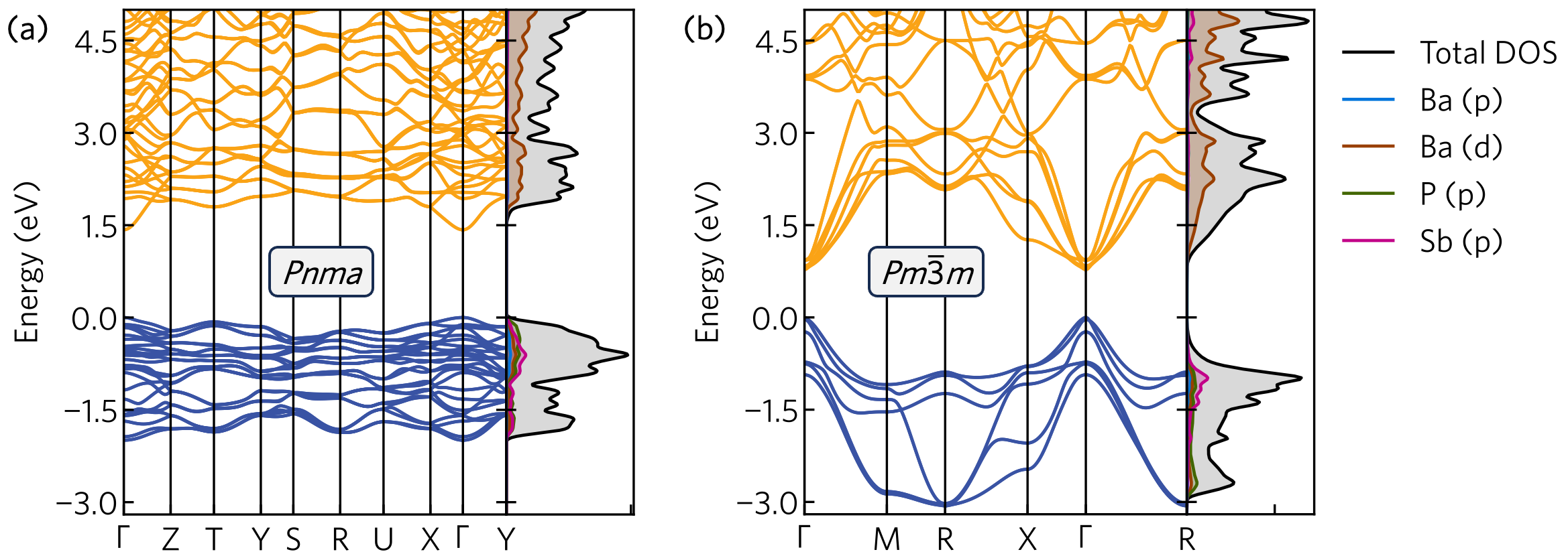
To understand the trend in the band gaps of the series, we examine the orbital contributions at the band edges. The orbital-projected density of states of \ceBa3SbP, calculated using HSE+SOC is presented in Fig. 3a. Similar to the nitride antiperovskites, the Sb site plays a critical role in the frontier orbitals at the band edges.16 This is in contrast to the conventional perovskites, in which the species on the cuboctahedral site are typically spectator ions whose role is to charge balance the composition and provide structural support for the octahedral cages. The valence band maximum is composed of P 3p and Sb 5p states, whereas the conduction band minimum is almost entirely composed of the Ba 5d orbitals. The conduction band states are particularly delocalised, as demonstrated by the charge density isosurfaces displayed in Section S4 of the Supplementary Information, and give rise to a relatively disperse band. As we shall demonstrate later through analysis of the bulk band alignment, the band gap change down the series is largely driven by a shift in the valence band maximum, with the conduction band minimum remaining roughly fixed. The valence band shift is controlled by two competing factors: i) the bandwidth of the valence band states, which decreases down the series due to the increased bond lengths (from for Ca to for Ba) and which acts to open the band gap. ii) The Madelung energies at the Sb and P sites which comprise the valence band edge, which decrease down the series due to the greater octahedral distortions (see Supplementary Table S7 for the tabulated Madelung energies) and which act to lower the band gap. Finally, we note that spin–orbit coupling has a small but non-negligible impact on the electronic structure, with relativistic renormalisation of (Ca), (Sr), and (Ba). The diminishing impact of SOC down the group can be attributed to the shrinking contributions of the Sb 5p states — the only frontier orbitals experiencing strong SOC — at the valence band edge down the series due to increased tilting (as revealed in the charge density isosurfaces presented in Fig. S3 of the Supplementary Information).
| Compound | IP | EA | ||||||||||
|---|---|---|---|---|---|---|---|---|---|---|---|---|
| \ceCa3SbP | 1.07 | 0.22 | 0.38 | 4.9 | 29.7 | 1.63 | 0.38 | 0.67 | 7.5 | 23.9 | 2.86 | 1.23 |
| \ceSr3SbP | 0.85 | 0.21 | 0.11 | 4.7 | 28.0 | 1.62 | 0.45 | 0.22 | 6.9 | 27.2 | 2.70 | 1.09 |
| \ceBa3SbP | 0.78 | 0.16 | 0.16 | 4.3 | 27.0 | 1.43 | 0.93 | 0.28 | 3.6 | 31.4 | 2.57 | 1.14 |
To better understand the nature of carrier transport in \ce3SbP, we calculate band edge effective masses using the sumo package.34 The effective masses of the valence band maximum and conduction band minimum are listed in Table 1. The electron effective masses were found to be relatively light and range from (Ca) to (Sr) and (Ba), as expected based on the dispersive charge density isosurfaces in Fig. S4 of the Supplementary Information. This is comparable to the antiperovskite nitrides \ceSr3SbN () and \ceBa3SbN ()16, and other more established photovoltaic absorbers, such as \ceCH3NH3PbI3 ( = )44 and CdTe (). Small effective masses improve the collection efficiency of photoexcited carriers and typically result in large polarons, weakly bound excitons,45 and small defect capture cross sections.46. The hole effective masses are somewhat larger, ranging from across the series. We note that the effective masses are reasonably anisotropic, particularly for holes, as demonstrated in Table S10 of the Supplementary Information.
We find that the orthorhombic phase undergoes significant charge localisation compared to the cubic structure. Primarily, this can be seen in the bandwidth of the upper valence band which reduces from over in the cubic phase to in the orthorhombic phase for \ceBa3SbP (Fig. 3). A similar effect can be observed in the conduction band and persists for the other compounds in the series. This localisation widens the band gap from to and increases the electron effective masses from to in the case of the Ba analogue. This effect is well known in the conventional and hybrid perovskites and originates from increased octahedral tilting that decreases the overlap between the orbitals comprising the band edges.47 We note, however, that this localisation acts to increase the band gaps of the series into the ideal range for efficient solar absorbers () and thus may be beneficial for photovoltaic device performance.
3.3 Optical absorption and predicted photovoltaic efficiency
Beyond an appropriate band gap and light charge carriers, strong visible light absorption is essential for efficient photovoltaics. The optical absorption of \ce3SbP calculated using HSE+SOC is presented in Fig. 4a. All three materials exhibit a steep absorption onset, quickly reaching greater than within less than of the fundamental band gap. The strength of the absorption can be attributed to the double degeneracy of the highest valence band and lowest conduction band. \ceBa3SbP displays the strongest absorption onset, in part due to the more localised valence band edge which increases the joint density of states. In contrast, \ceCa3SbP exhibits the slowest absorption onset due to its disperse valence band. The absorption for the series is competitive with other thin-film absorbers such as \ceCH3NH3PbI3 and CdTe, and is considerably stronger silicon due to its indirect band gap.48
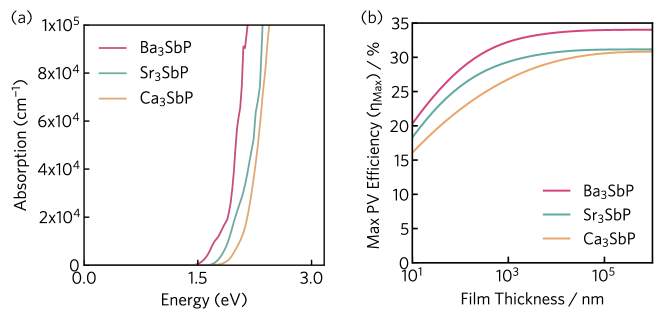
To assess the potential of the \ce3SbP series in photovoltaic devices, we calculate the maximum theoretical efficiency using the detailed balance metric developed by Blank et al. 36 This approach goes beyond the standard Shockley–Queisser limit49 by taking into account the full optical response and distinguishing external luminescence yield from internal radiative recombination. We model a Lambertian surface that reduces losses through a diffusely scattering front surface and a back surface with unity reflectance. The theoretical efficiencies were obtained using the frequency-dependent dielectric response calculated using HSE+SOC. The theoretical efficiency strongly depends on the thickness of the absorber layer and reaches a maximum value of (Ca, Sr) and (Ba) in the high thickness limit. For films (as commonly used in thin-film photovoltaics), the efficiency is found to be (Ca), (Sr), and (Ba). This is noticeably larger than predicted for \ceSr3SbN and \ceBa3SbN ( and , respectively16), and competitive with other emerging antimony absorbers such as \ceSn2SbS2I3 ().50 It is important to stress that the Blank metric provides an upper limit to the photovoltaic performance. In practical devices, the efficiency will be reduced through non-radiative recombination and contact losses at interfaces. Regardless, our results highlight the potential of \ce3SbP as photovoltaic absorbers.
3.4 Band alignment
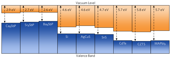
Photovoltaic devices with high performance require electron and hole contact materials with suitable alignments to the valence and conduction bands of the absorber. An efficient alignment prevents open-circuit voltage losses and minimises barriers for carrier diffusion at the interfaces. To provide insight into ideal device architectures, we perform band alignment calculations using a slab–vacuum model. Our calculations aim to understand the “bulk” band alignment — namely, they do not take into account relaxations and band bending at the surface. We calculate ultra-low ionisation potentials and electron affinities of and , respectively. We find the depth of the conduction band remains roughly fixed down the series, whereas the valence band edge is raised monotonically from Ca to Ba. Our calculated band offsets are roughly smaller than those found in the nitride antiperovskites.16 For example, Kang 16 calculated an ionisation potential and electron affinity of and for \ceSr3SbN, using a slab–vaccuum approach with PBE+SOC. The origin of this shift can be attributed to the greater electronegativity of nitrogen, which acts to push the valence band further from the vacuum level. In Fig. 5, we compare the band alignment of the series to a range of conventional and emerging photovoltaic absorbers. We find the ionisation potentials of \ce3SbP to be considerably smaller than any other commonly used absorber, for example Si and AgCuS which are closest in magnitude at .
The shallow ionisation potentials and electron affinities will require careful choice of contact materials to maximise the obtainable open circuit voltage. Efficient devices require the work function () of the transparent electron contact to be greater than the electron affinity of the absorber. Conversely, the workfunction of the hole transport material should be smaller than the ionisation potential of the absorber. Most -type transparent conductors have deep workfunctions (greater than ) and therefore will not be suitable for the phosphide antiperovskites. Accordingly, ultra-low workfunction electron contact materials such as the semiconducting polymer TPHP(\ceLiClO4) ( = ) should be employed.55 For hole extraction, a low workfunction metal alloy such as MgNd ( = ) may be appropriate.56
4 Conclusion
We evaluated the \ce3SbP antiperovskites (where A = Ca, Sr, Ba) as potential photovoltaics using relativistic hybrid density functional theory calculations. In contrast to previous reports,21 we demonstrate the cubic phase is likely unstable and will spontaneously distort to an orthorhombic structure. We evaluate the thermodynamic stability of this phase against other antiperovskite-like compositions and reveal that it is dynamically stable, with no imaginary modes found in the phonon band structure. The series possesses ideal band gaps between , with small electron effective masses, and strong visible light absorption. The predicted maximum theoretical efficiencies of for thin films are competitive with other state-of-the-art and emerging absorbers. Furthermore, we performed band alignment calculations to recommend hole and electron contact materials that will provide efficient charge extraction in optimised devices. We believe that the \ce3SbP series show potential as photovoltaic absorbers and should be targeted for experimental verification.
5 Author Contributions
CRediT system for author contributions: https://credit.niso.org Ruiqi Wu: Investigation, Formal Analysis, Methodology, Visualization, Writing – original draft, Writing – review & editing. Alex Ganose: Conceptualization, Methodology, Resources, Supervision, Writing – review & editing.
6 Acknowledgements
A.M.G. was supported by EPSRC Fellowship EP/T033231/1. We are grateful to the UK Materials and Molecular Modelling Hub for computational resources, which is partially funded by EPSRC (EP/P020194/1 and EP/T022213/1). This work used the ARCHER2 UK National Supercomputing Service (https://www.archer2.ac.uk) via our membership of the UK’s HEC Materials Chemistry Consortium, which is funded by EPSRC (EP/L000202).
References
- 1 Kamaya, N.; Homma, K.; Yamakawa, Y.; Hirayama, M.; Kanno, R.; Yonemura, M.; Kamiyama, T.; Kato, Y.; Hama, S.; Kawamoto, K.; Mitsui, A. A Lithium Superionic Conductor. Nature Mater. 10, 682–686
- 2 Kamishima, K.; Goto, T.; Nakagawa, H.; Miura, N.; Ohashi, M.; Mori, N.; Sasaki, T.; Kanomata, T. Giant Magnetoresistance in the Intermetallic Compound Mn3GaC. Phys. Rev. B 63, 024426
- 3 Bauer, E.; Hilscher, G.; Michor, H.; Paul, C.; Scheidt, E.-W.; Gribanov, A.; Seropegin, Y.; Noël, H.; Sigrist, M.; Rogl, P. Heavy Fermion Superconductivity and Magnetic Order in CsPt3Si. Phys. Rev. Lett. 92, 027003
- 4 Chen, J.; Hu, L.; Deng, J.; Xing, X. Negative Thermal Expansion in Functional Materials: Controllable Thermal Expansion by Chemical Modifications. Chem. Soc. Rev. 44, 3522–3567
- 5 Luo, H.; Liu, J.; Zheng, X.; Han, L.; Ren, K.; Yu, X. Enhanced Photoluminescence of Sr3SiO5:Ce3+ and Tuneable Yellow Emission of Sr3SiO5:Ce3+,Eu2+ by Al3+ Charge Compensation for W-LEDs. J. Mater. Chem. 22, 15887–15893
- 6 Jia, X.; Zhao, Y.; Chen, G.; Shang, L.; Shi, R.; Kang, X.; Waterhouse, G. I. N.; Wu, L.-Z.; Tung, C.-H.; Zhang, T. Ni3FeN Nanoparticles Derived from Ultrathin NiFe-Layered Double Hydroxide Nanosheets: An Efficient Overall Water Splitting Electrocatalyst. Adv. Energy Mater. 6, 1502585
- 7 Zhao, Y.; Daemen, L. L. Superionic Conductivity in Lithium-Rich Anti-Perovskites. J. Am. Chem. Soc. 134, 15042–15047
- 8 Chen, L.; Luo, A.; Jiang, Y.; Liu, F.; Deng, X.; Xue, S.; Chen, X.; Zhang, Y. Suppressing the Phase Transformation and Enhancing the Orange Luminescence of (Sr,Ba)3SiO5:Eu2+ for Application in White LEDs. Mater. Lett. 106, 428–431
- 9 Vaughn II, D. D.; Araujo, J.; Meduri, P.; Callejas, J. F.; Hickner, M. A.; Schaak, R. E. Solution Synthesis of Cu3PdN Nanocrystals as Ternary Metal Nitride Electrocatalysts for the Oxygen Reduction Reaction. Chem. Mater. 26, 6226–6232
- 10 Zhao, Y.; Ma, F.; Qu, Z.; Yu, S.; Shen, T.; Deng, H.-X.; Chu, X.; Peng, X.; Yuan, Y.; Zhang, X.; You, J. Inactive (PbI2)2RbCl Stabilizes Perovskite Films for Efficient Solar Cells. Science 377, 531–534
- 11 Wang, Y.; Zhang, H.; Zhu, J.; Lü, X.; Li, S.; Zou, R.; Zhao, Y. Antiperovskites with Exceptional Functionalities. Adv. Mater. 32, 1905007
- Fabini et al. 2019 Fabini, D. H.; Koerner, M.; Seshadri, R. Candidate inorganic photovoltaic materials from electronic structure-based optical absorption and charge transport proxies. Chem. Mater. 2019, 31, 1561–1574
- Kuhar et al. 2018 Kuhar, K.; Pandey, M.; Thygesen, K. S.; Jacobsen, K. W. High-throughput computational assessment of previously synthesized semiconductors for photovoltaic and photoelectrochemical devices. ACS Energy Lett. 2018, 3, 436–446
- 14 Heinselman, K. N.; Lany, S.; Perkins, J. D.; Talley, K. R.; Zakutayev, A. Thin Film Synthesis of Semiconductors in the Mg–Sb–N Materials System. Chem. Mater. 31, 8717–8724
- 15 Mochizuki, Y.; Sung, H.-J.; Takahashi, A.; Kumagai, Y.; Oba, F. Theoretical Exploration of Mixed-Anion Antiperovskite Semiconductors M3XN (M = Mg , Ca , Sr , Ba ; X = P , As , Sb , Bi). Phys. Rev. Materials 4, 044601
- Kang 2022 Kang, Y. Antiperovskite Sr3MN and Ba3MN (M = Sb or Bi) as promising photovoltaic absorbers for thin-film solar cells: A first-principles study. J. Am. Ceram. Soc. 2022, 105, 5807–5816
- 17 Kang, Y. Native Point Defects in Antiperovskite Ba3SbN: A Promising Semiconductor for Photovoltaics. Phys. Chem. Chem. Phys. 25, 9800–9806
- Sreedevi et al. 2022 Sreedevi, P.; Vidya, R.; Ravindran, P. Antiperovskite materials as promising candidates for efficient tandem photovoltaics: First-principles investigation. Mater. Sci. Semicond. Process. 2022, 147, 106727
- Han et al. 2021 Han, D.; Feng, C.; Du, M.-H.; Zhang, T.; Wang, S.; Tang, G.; Bein, T.; Ebert, H. Design of High-Performance Lead-Free Quaternary Antiperovskites for Photovoltaics via Ion Type Inversion and Anion Ordering. J. Amer. Chem. Soc. 2021, 143, 12369–12379
- Guo et al. 2023 Guo, Y.; Liu, X.; Wang, H.; Zang, Z.; Li, R. High-performance lead-free quaternary antiperovskite photovoltaic candidate Ca6N2AsSb. Phys. Chem. Chem. Phys. 2023, 25, 17112–17115
- 21 Liang, Q.-Q.; Hu, D.-Y.; Zhao, X.-H.; Tang, T.-Y.; Gao, H.-X.; Wu, S.-Q.; Tang, Y.-L. Predicting the Structural, Elastic, Electronic, and Optical Properties of Anti-Perovskites X3SbP (X = Ca, Sr, Ba) via First-Principles. Chem. Phys. Lett. 808, 140127
- 22 Kohn, W.; Sham, L. J. Self-Consistent Equations Including Exchange and Correlation Effects. Phys. Rev. 140, A1133–A1138
- 23 Kresse, G.; Furthmüller, J. Efficiency of Ab-Initio Total Energy Calculations for Metals and Semiconductors Using a Plane-Wave Basis Set. Comput. Mater. Sci. 6, 15–50
- 24 Kresse, G.; Hafner, J. Ab Initio Molecular Dynamics for Liquid Metals. Phys. Rev. B 47, 558–561
- 25 Kresse, G.; Hafner, J. Ab Initio Molecular-Dynamics Simulation of the Liquid-Metal–Amorphous-Semiconductor Transition in Germanium. Phys. Rev. B 49, 14251–14269
- 26 Kresse, G.; Joubert, D. From Ultrasoft Pseudopotentials to the Projector Augmented-Wave Method. Phys. Rev. B 59, 1758–1775
- 27 Perdew, J. P.; Ruzsinszky, A.; Csonka, G. I.; Vydrov, O. A.; Scuseria, G. E.; Constantin, L. A.; Zhou, X.; Burke, K. Restoring the Density-Gradient Expansion for Exchange in Solids and Surfaces. Phys. Rev. Lett. 100, 136406
- 28 Perdew, J. P.; Burke, K.; Ernzerhof, M. Generalized Gradient Approximation Made Simple. Phys. Rev. Lett. 77, 3865–3868
- 29 Krukau, A. V.; Vydrov, O. A.; Izmaylov, A. F.; Scuseria, G. E. Influence of the Exchange Screening Parameter on the Performance of Screened Hybrid Functionals. J. Chem. Phys. 125, 224106
- 30 Heyd, J.; Scuseria, G. E.; Ernzerhof, M. Hybrid Functionals Based on a Screened Coulomb Potential. J. Chem. Phys 118, 8207–8215
- Wang et al. 2022 Wang, X.; Li, Z.; Kavanagh, S. R.; Ganose, A. M.; Walsh, A. Lone Pair Driven Anisotropy in Antimony Chalcogenide Semiconductors. Phys. Chem. Chem. Phys. 2022, 24, 7195–7202
- 32 Park, J.; Xia, Y.; Ganose, A. M.; Jain, A.; Ozoliņš, V. High Thermoelectric Performance and Defect Energetics of Multipocketed Full Heusler Compounds. Phys. Rev. Appl. 14, 024064
- Ganose et al. 2018 Ganose, A. M.; Matsumoto, S.; Buckeridge, J.; Scanlon, D. O. Defect Engineering of Earth-Abundant Solar Absorbers BiSI and BiSeI. Chem. Mater. 2018, 30, 3827–3835
- 34 Alex, M. G.; Adam, J. J.; David, O. S. Sumo: Command-line Tools for Plotting and Analysis of Periodic Ab Initio Calculations. J. Open Source Softw. 3, 717
- 35 Gajdoš, M.; Hummer, K.; Kresse, G.; Furthmüller, J.; Bechstedt, F. Linear Optical Properties in the Projector-Augmented Wave Methodology. Phys. Rev. B 73, 045112
- 36 Blank, B.; Kirchartz, T.; Lany, S.; Rau, U. Selection Metric for Photovoltaic Materials Screening Based on Detailed-Balance Analysis. Phys. Rev. Appl. 8, 024032
- 37 Brlec, K.; Davies, D. W.; Scanlon, D. O. Surfaxe: Systematic Surface Calculations. J. Open Source Softw. 6, 3171
- 38 Togo, A. First-Principles Phonon Calculations with Phonopy and Phono3py. J. Phys. Soc. Jpn. 92, 012001
- 39 Goldschmidt, V. M. Die Gesetze der Krystallochemie. Naturwissenschaften 14, 477–485
- 40 Shannon, R. D. Revised Effective Ionic Radii and Systematic Studies of Interatomic Distances in Halides and Chalcogenides. Acta Cryst A 32, 751–767
- 41 Rahim, W.; Skelton, J. M.; Savory, C. N.; Evans, I. R.; Evans, J. S. O.; Walsh, A.; Scanlon, D. O. Polymorph Exploration of Bismuth Stannate Using First-Principles Phonon Mode Mapping. Chem. Sci. 11, 7904–7909
- 42 Pham, T.-L.; Samad, A.; Kim, H. J.; Shin, Y.-H. Computational Predictions of Stable Phase for Antiperovskite Na3OCl via Tilting of Na6O Octahedra. Journal of Applied Physics 124, 164106
- Chen et al. 2015 Chen, M.-H.; Emly, A.; Van der Ven, A. Anharmonicity and phase stability of antiperovskite Li3OCl. Phys. Rev. B 2015, 91, 214306
- Frost et al. 2014 Frost, J. M.; Butler, K. T.; Brivio, F.; Hendon, C. H.; van Schilfgaarde, M.; Walsh, A. Atomistic Origins of High-Performance in Hybrid Halide Perovskite Solar Cells. Nano Lett. 2014, 14, 2584–2590
- Walsh and Zunger 2017 Walsh, A.; Zunger, A. Instilling Defect Tolerance in New Compounds. Nature Mater. 2017, 16, 964–967
- Huang et al. 2022 Huang, Y.; Yuan, H.; Chen, H. High-Performance Thermoelectrics in Two-Dimensional Layered AB2Te4 (A=Sn, Pb; B=Sb, Bi) Ternary Compounds. Phys. Chem. Chem. Phys. 2022,
- Mannino et al. 2020 Mannino, G.; Deretzis, I.; Smecca, E.; La Magna, A.; Alberti, A.; Ceratti, D.; Cahen, D. Temperature-Dependent Optical Band Gap in CsPbBr3, MAPbBr3, and FAPbBr3 Single Crystals. J. Phys. Chem. Lett. 2020, 11, 2490–2496
- De Wolf et al. 2014 De Wolf, S.; Holovsky, J.; Moon, S.-J.; Löper, P.; Niesen, B.; Ledinsky, M.; Haug, F.-J.; Yum, J.-H.; Ballif, C. Organometallic Halide Perovskites: Sharp Optical Absorption Edge and Its Relation to Photovoltaic Performance. J. Phys. Chem. Lett. 2014, 5, 1035–1039
- 49 Shockley, W.; Queisser, H. J. Detailed Balance Limit of Efficiency of P-n Junction Solar Cells. J. Appl. Phys. 32, 510–519
- Kavanagh et al. 2021 Kavanagh, S. R.; Savory, C. N.; Scanlon, D. O.; Walsh, A. Hidden Spontaneous Polarisation in the Chalcohalide Photovoltaic Absorber Sn2SbS2I3. Mater. Horiz. 2021, 8, 2709–2716
- Burton and Walsh 2013 Burton, L. A.; Walsh, A. Band Alignment in SnS Thin-Film Solar Cells: Possible Origin of the Low Conversion Efficiency. Appl. Phys. Lett. 2013, 102, 132111
- Brgoch et al. 2014 Brgoch, J.; Lehner, A. J.; Chabinyc, M.; Seshadri, R. Ab Initio Calculations of Band Gaps and Absolute Band Positions of Polymorphs of RbPbI3 and CsPbI3: Implications for Main-Group Halide Perovskite Photovoltaics. J. Phys. Chem. C 2014, 118, 27721–27727
- Savory et al. 2016 Savory, C. N.; Ganose, A. M.; Travis, W.; Atri, R. S.; Palgrave, R. G.; Scanlon, D. O. An Assessment of Silver Copper Sulfides for Photovoltaic Applications: Theoretical and Experimental Insights. J. Mater. Chem. A 2016, 4, 12648–12657
- Walsh 2015 Walsh, A. Principles of Chemical Bonding and Band Gap Engineering in Hybrid Organic–Inorganic Halide Perovskites. J. Phys. Chem. C 2015, 119, 5755–5760
- Tong et al. 2022 Tong, B.; Du, J.; Yin, L.; Zhang, D.; Zhang, W.; Liu, Y.; Wei, Y.; Liu, C.; Liang, Y.; Sun, D.-M.; Ma, L.-P.; Cheng, H.-M.; Ren, W. A Polymer Electrolyte Design Enables Ultralow-Work-Function Electrode for High-Performance Optoelectronics. Nat. Commun. 2022, 13, 4987
- Ge et al. 2018 Ge, K.; Chen, J.; Chen, B.; Shen, Y.; Guo, J.; Li, F.; Liu, H.; Xu, Y.; Mai, Y. Low Work Function Intermetallic Thin Film as a Back Surface Field Material for Hybrid Solar Cells. Solar Energy 2018, 162, 397–402