Electronic and optical properties of boron containing GaN alloys: The role boron atom clustering
Abstract
Boron (B) containing III-nitride materials, such as wurtzite (B,Ga)N alloys, have recently attracted significant interest to tailor the electronic and optical properties of optoelectronic devices operating in the visible and ultraviolet spectral range. However, the growth of high quality samples is challenging and B atom clustering is often observed in (B,Ga)N alloys. To date, fundamental understanding of the impact of such clustering on electronic and optical properties of these alloys is sparse. In this work we employ density functional theory (DFT) in the framework of the meta generalized gradient approximation (modified Becke Johnson (mBJ) functional) to provide insight into this question. We use mBJ DFT calculations, benchmarked against state-of-the-art hybrid functional DFT, on (B,Ga)N alloys in the experimentally relevant B content range of up to 7.4%. Our results reveal that B atom clustering can lead to a strong reduction in the bandgap of such an alloy, in contrast to alloy configurations where B atoms are not forming clusters, thus not sharing nitrogen (N) atoms. We find that the reduction in bandgap is linked mainly to carrier localization effects in the valence band, which stem from local strain and polarization field effects. However, our study also reveals that the alloy microstructure of a B atom cluster plays an important role: B atom chains along the wurtzite axis impact the electronic structure far less strongly when compared to a chain formed within the -plane. This effect is again linked to local polarization field effects and the orbital character of the involved valence states in wurtzite BN and GaN. Overall, our calculations show that controlling the alloy microstructure of (B,Ga)N alloys is of central importance when it comes to utilizing these systems in future optoelectronic devices with improved efficiencies.
The direct bandgap III-nitride semiconductor family (AlN, GaN and InN) and their connected alloys, (Al,Ga,In)N, have attracted great interest for achieving energy efficient optoelectronic devices such as light emitting diodes (LEDs) [1, 2]. In principle, by tailoring the alloy content in the active region of a device, the emission wavelength can range from the deep ultraviolet (UV) to the red [2, 3, 4]. However, both (deep) UV emitters utilizing (Al,Ga)N [5, 6, 7, 8] and red emitters based on (In,Ga)N [9, 10, 11] suffer from low quantum efficiencies [12, 7, 8, 13]. Several factors contribute to these low efficiencies in the short and long wavelength window, including the large lattice mismatch in heterostructures, lattice mistmatch with the underlying substrate as well as fundamental changes in the (valence) band structure [14]. To address these challenges, boron (B) containing nitride alloys have garnered significant interest in recent years. The aim is to utilise the smaller lattice parameter of wurtzite (wz) BN in comparison to (Al, Ga, In)N to create quantum-well (QW) structures with reduced lattice mismatch and to control the valence band structure [15, 16, 17, 13, 18]. Ideally, controlling the strain in the system should reduce built-in polarization fields but also lattice mismatch related defect densities.
However, growth of high quality B containing III-N alloys and heterostructures presents a serious challenge. There are two main reasons for this: (i) B atoms are dissimilar from other group III elements in terms of size and electronegativity and (ii) the ground state crystal structure of BN is hexagonal, while AlN, GaN and InN preferentially crystallize in the wz phase. Due to this and the low miscibility of BN with (Al,Ga,In)N [13], only small amounts (10%) of B can be incorporated into e.g. wz (B,Ga)N alloys [16, 19, 18, 20, 21], as the material undergoes a spinodal phase-degradation at higher BN contents [16]. While high-quality, crystalline random alloys of (B,Ga)N with a B content around 3% have been reported [20], experimental data indicates a tendency of B atom clustering in such alloys [21]. However, the impact of such clustering effects on the electronic and optical properties is largely unexplored.
To exploit the full potential benefit of B containing III-N alloys and heterostructures, fundamental understanding of the impact of B on the electronic and optical properties of such alloys is needed. But, in comparison to experimental studies, theoretical investigations on B containing III-N alloys are sparse and their focus is mainly on bandgap bowing parameters, miscibility limits or the direct-indirect bandgap crossover [22, 23, 24, 15, 17] when assuming random alloys.
Clustering of B atoms in III-N alloys has been largely overlooked as bigger simulation cells are required to address experimentally relevant low B concentrations and to capture potential carrier localization effects. These larger cells often present huge computational challenges for state-of-the-art first principle methods, such as Heyd, Scuseria and Ernzerhof (HSE) hybrid functional density functional theory (HSE-DFT) [25, 26]. For example, Shen et al. [24] and Turiansky et al. [22] study the bandgap bowing in (B,Al)N and (B,Ga)N alloys, respectively, using HSE-DFT. They account for alloy fluctuations by creating ten random alloy configurations for different B concentrations in a 72 atom supercell, which allows a statistical approach to account for the changes in material properties caused by different alloy distributions. Williams and Kioupakis [17] study quaternary (B,Al,Ga)N alloys using special quasi random structures (SQS), to provide insight into the impact of random alloy fluctuations on the electronic structure. While their work provides a general understanding of the material properties, it does not shed light on deviations (e.g. clustering) from a random alloy configuration.
Recently, an alternative to HSE-DFT has emerged, namely the meta generalised gradient approximation (meta-GGA), which is significantly less resource intensive but produces comparative results, especially for bandgaps [27]. Meta-GGAs incorporate the kinetic energy density in addition to the density gradient, which alleviates the effects of the self-interaction error [28, 29] that causes bandgap underestimation in traditional GGA potentials [30, 31, 32].
In this study, we apply modified Becke-Johnson (mBJ) meta-GGA to study the effects of B atom clustering on the electronic structure of wz (B,Ga)N; we also demonstrate (see Supplemental Information (SI)) that mBJ reproduce HSE-DFT band structures in the region of interest (e.g. - and -point) of wz-BN, AlN, GaN and InN with good accuracy. In the following, all results and discussions will focus on wz III-N, unless otherwise specified. Overall, our findings show that the alloy microstructure significantly affects the electronic and optical properties of (B,Ga)N alloys with B contents up to the here-considered 7.4%. For instance, we find that for a fixed B content in a (B,Ga)N alloy, clustering of B atoms (B atoms sharing N atoms) can reduce the bandgap drastically compared to configurations in the absence of such clustering. This observed reduction in bandgap is mainly linked to carrier localization effects in the valence band, which we attribute to local strain and polarization field effects introduced by B atom clustering; such carrier localization effects are not observed when the B atoms are evenly distributed.
Methods: All calculations were carried out with DFT as implemented in the Vienna ab initio Simulation Package (VASP) v5.4 [33]. Models and charge densities were visualised using VESTA [34]. When evaluating the band structures of pristine wz GaN and BN, we used a -centred Monkhorst-pack k-point mesh of 664, Gaussian smearing of = 0.1 eV, and a plane wave cut-off energy of 600 eV. The convergence criteria were eV for the energy minimisation and 0.02 eV/Å for the forces in the ionic relaxations. The valence electrons for all atom types and the semicore -electrons for Ga are described explicitly by expanding their wave function in a plane wave basis set, while the core electrons are treated by PAW potentials [35, 36]. For our DFT investigations we used HSE functionals [26] as a reference for mBJ meta-GGA [37, 38] calculations. As mBJ meta-GGA does not allow structural relaxations, the generalized gradient approximation (GGA), as implemented in the Perdew-Burke-Ernzerhof (PBE) exchange-correlation functional [39], was used for lattice and geometry relaxations. All electronic structure calculations presented below utilize mBJ meta-GGA [37]. Further information on our HSE-DFT and mBJ meta-GGA benchmark are given in the SI.
To study the impact of B atom clustering on the electronic and optical properties of (B,Ga)N alloys, we used a (333) supercell that contains 108 atoms. One to four Ga atoms were replaced with B atoms in various configurations (see below), which corresponds to B contents ranging from 2 to 7%. For the (B,Ga)N structures, the lattice parameters as well as internal degrees of freedom of the atoms in the simulation cell were optimised until the pressure on the system was minimised. We note that the lattice parameters obtained with this method deviate from the lattice parameters predicted based on a linear interpolation (Vegard’s approximation) by no more than 0.7%. Also, the introduction of B atoms into GaN did not cause any major changes in the crystal structure (no phase change).
Results and Discussion: To achieve a thorough understanding of the effect of B atom clustering on the electronic structure of (B,Ga)N alloys, we study an array of different alloy arrangements of up to four B atoms (visual representations of these configurations are included in the SI):
-
•
Close: 3 or 4 B atoms substituted at cation sites around a single N, i.e. in case of 4 B atoms a full tetrahedron is formed.
-
•
Apart: 2, 3 or 4 B atoms substituted with the maximum number of cation sites between them so that they are not sharing a N atom.
-
•
Line: 2, 3 or 4 B atoms substituted at adjacent cation sites always connected by a N atom in the same -plane.
-
•
z-Line: 2 or 4 B atoms substituted vertically in a zig-zag along the -axis (i.e., one or two unit cells of BN stacked on top of each other).
-
•
2 1: 2 B sharing an N atom with a third B atom at the next nearest cation site in the same layer (same -plane) as one of the B atoms.
-
•
2 2 Close: two 2 B z-line configurations at next-nearest cation sites in the same plane.
-
•
2 2 Apart: two 2 B z-line configurations at cation sites that are as far away from each other as possible.
-
•
3 1: a 3 B close configuration with an additional fourth B atom at the next nearest cation site in the same layer as the B atom at the top of the tetrahedron containing the 3 B atoms.
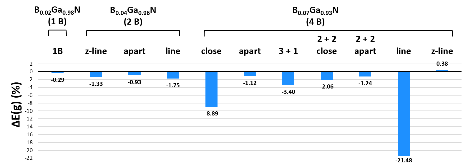
Figure 1 shows the relative change in bandgap for the different alloy configurations in the studied (B,Ga)N alloys with respect to pristine GaN. In the following we focus mainly on the configurations with a single, 2 and 4 B atoms to discuss trends in the electronic and optical properties. Detailed information on the system with 3 B atoms can be found in the SI, with additional information on the bandgap changes and lattice constant variations for all configurations.
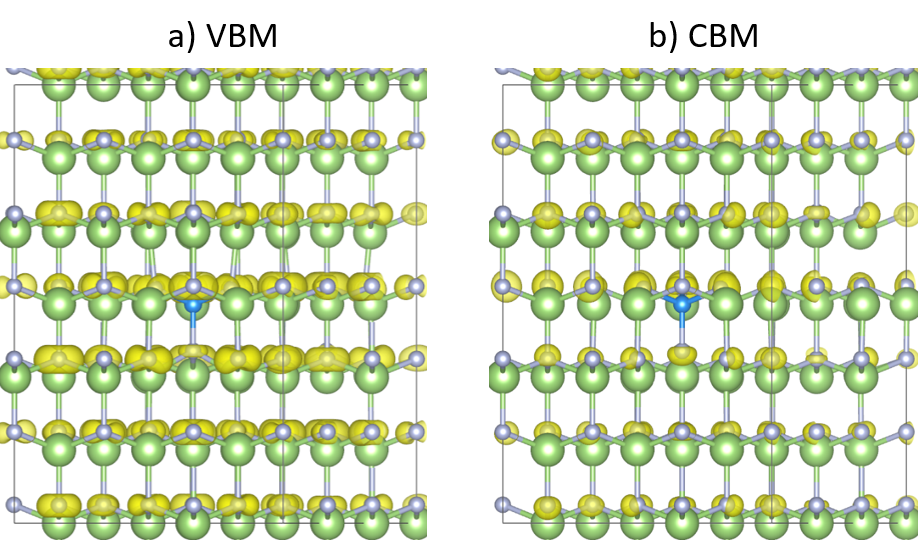
For the single B atom ( 2% B content), we find that the bandgap is not significantly changed. The charge densities, Fig. 2, of the conduction band minimum (CBM) and valence band maximum (VBM) of this configuration show that the electronic structure is only weakly perturbed by an isolated B atom in GaN. This finding is also observed when studying larger B contents and assuming that B atoms are not sharing N atoms (”apart” in Fig. 1): the bandgap changes by only % regardless of B content.
However, in alloy configurations where B atoms are clustering and thus sharing N atoms, the bandgap of a (B,Ga)N alloy is more significantly affected. In general, this effect increases in magnitude with increasing B content as Fig. 1 reveals (see also SI for 3 B atom case). For example, the change in bandgap for 2 B atoms sharing a N atom can be %, while for 4 B atoms sharing the same N atom the change is % (for 3 B atoms the change in bandgap is %, see SI) when compared to pure GaN. Moreover, this bandgap reduction also depends on the orientation of the B atoms with respect to each other. In the 2 B system, the change in bandgap is slightly larger (%) for B atoms in the same -plane (”line” configuration in Fig. 1) when compared to B atoms oriented along the -axis (%; -line configuration in Fig. 1). This effect is dramatically increased in the 4 B atom case. In the ”line” configuration the bandgap is changed by % (reduction in bandgap compared to pure GaN) while in the ”-line” arrangement the bandgap changes by % (slight increase in the bandgap when compared to pure GaN).
Overall, Fig. 1 shows that, with the exception of the -line configuration, the bandgap decreases when B atoms are incorporated in GaN; this statement also holds for the 3 B atom case (see SI). Previous calculations [22] on the bandgap of (B,Ga)N suggest that the change in bandgap is minimal in the low B content regime (%), and that the bandgap is expected to widen, not shrink, with increasing B content. However, we note that in Ref. [22] (i) a random alloy is assumed and (ii) the supercells studied are smaller (, thus 72 atoms) when compared to our systems (, thus 108 atoms). Therefore, B atom clustering as considered in our work for low B contents (up to 7%) is most likely not resolved in Ref. [22]. Additionally, the shorter supercell size along the -axis considered in Ref. [22] may provide a preference for electronic coupling of B atoms along the -axis similar to our ”z-line” configuration. All these factors may explain the differences and similarities in the bandgap evolution in (B,Ga)N alloys observed in our work and Ref. [22]. On the other hand, recent experimental work on 500 nm (B,Ga)N epilayers grown on GaN/sapphire showed that in (B,Ga)N/GaN systems with a B content of up to 3% a reduction in bandgap of 0.03 to 0.04 eV occurs [18]. According to the findings in Ref. [18], this effect stems from shifts in the valence band of the studied (B,Ga)N alloys. A direct comparison between our results and the experimental data however is in general not possible since further information on the alloy microstructure and the strain state of the sample would be required. Nevertheless, the experimental data gives first indications that in the low B content regime a shrinkage of the (B,Ga)N bandgap may be observed. Furthermore, previous experimental studies also indicated B atom clustering in (B,Ga)N alloys [21]. Our results above show that a bandgap reduction can be promoted by B atom clustering. However, the bandgap of wz-BN is larger than GaN, and the natural valence band offset between the two binary materials is negative (VBE in BN lower in energy when compared to GaN) and large ( eV) [40]. Based on these material properties alone, a widening of the bandgap may be expected when introducing BN into GaN. From our analysis in Fig. 1 we know this is not necessarily the case and it becomes clear that the electronic structure of (B,Ga)N alloys depends on the alloy microstructure. In the following we endeavour to explain why clustered B atoms have a vastly different impact on the band structure compared to distributed B atoms. To do this, it is useful to first review the fundamental band structure properties of BN and GaN.
Based on previous work [22, 41] on bulk GaN and BN, conduction band states of similar symmetry (-like in character) at the -point in BN and GaN are energetically far apart (¿ 5eV) when using the valence band offset of Dreyer et al. of eV [40]; furthermore the energetic separation of the conduction band edges (CBEs) in GaN (-point) and BN (-point) is 2 eV for the valence band offset from Ref. [40]. As such, when alloying GaN with BN, in the low B content regime one may expect that the CBE in (B,Ga)N is only weakly perturbed by the presence of B atoms in the lattice. In comparison the offset in the valence band is smaller, ( eV [40]) as mentioned above. Additionally, both GaN and BN exhibit a positive crystal field splitting energy at the -point (see also SI). Therefore, in both systems and when neglecting the weak spin-orbit coupling, the valence band edge (VBE) is - and -like in character, and the -like band is shifted to lower energy [22, 41, 42]. However, these are the properties of the ideal bulk materials. In a (B,Ga)N alloy local strain and built-in field effects will also contribute and can significantly change the electronic structure. Thus, we first analyse the charge densities of VBM and CBM obtained from DFT to determine whether changes to the electronic structure occur in CBM or VBM and to understand the impact of different alloy configurations on the electronic and ultimately optical properties of (B,Ga)N alloys at the atomic scale.
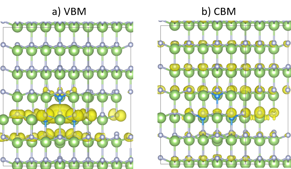
Figure 3 displays the band decomposed charge densities for 4 B atoms sharing the same N atom (thus forming a tetrahedron around the N atom, labeled as “close” in Fig. 1). The charge density of the CBM indicates a delocalized state that is only slightly affected by the presence of B atoms, in line with our discussion above. However, the VBM shows strong carrier localization effects on the N atom surrounded by B atoms. The 9% reduction in bandgap, Fig. 1, when B atoms cluster around a N atom, can thus be traced back to carrier localization effects in the valence band.
However, given the proposed band lineup between GaN and BN [40], such a localization effect may seem surprising at first glance. To gain further insight into the formation of such a localized valence state, and building on our DFT data, we have analyzed local strain and built-in field effects in more detail. First, we calculated a local strain tensor for the BN tetrahedron embedded in GaN; for detailed methodology and results, see SI. From our DFT simulations we find B-N bond lengths in pristine BN of Å, while Ga-N bonds in bulk GaN are 2.0 Å . In general, in the wz crystal structure of III-N materials, bonds along the -axis tend to have a slightly different length than those in the -plane. We find that for binary systems this difference is small (0.01 Å) but is quite pronounced in the alloys studied. Therefore, we distinguish between both types of bond lengths in the following. Our DFT calculations reveal that the B-N bonds in the 4 B tetrahedral (”close”) configuration are 22% longer when involving B atoms lying in the -plane and 9% longer along the -axis, all compared to a relaxed BN bulk system; thus the bonds exhibit tensile strain. Using this information we have calculated the local strain tensor around the N atom at the center of the 4 B cluster. This strain tensor is diagonal and we find and . Together with deformation potentials from the literature [41] and using theory [43] this strain tensor allows us to estimate changes in the valence band structure around the N atom. Based on this simple model, we find that and -like valence states are shifted to higher energies: the -like states will be shifted upward by 0.4 eV while the state is expected to be shifted by 1.5 eV with respect to their position in an unstrained BN bulk crystal. This may indeed indicate a localized state in the bandgap as a strain induced shift of 1.5 eV would exceed the valence band offset of eV [40]. However, one may expect that the localized state is -like in character, which is in contrast to the state predicted by our DFT calculations, see Fig. 3.

In general, III-N materials are polar semiconductors which exhibit, in comparison to other III-V materials, very strong electrostatic built-in polarization fields [44]. It has already been shown that local strain effects can lead to significant local polarization fields [45]. These local fields may then lead to strong carrier localization effects. Using a simple model (see SI) to gain insight in to this question, we found that the polarization vector field in the strained BN tetrahedron has the opposite direction and is also an order of magnitude larger than the polarization vector field in bulk GaN. Thus, the discontinuity in the polarization along the -axis can lead to an electrostatic built-in field along this direction which can then result in a strong (carrier) confinement. Given that in general -like valence states, in comparison to -like states, have a low effective mass along -axis (see for instance Ref. [43]), confinement due to local built-in fields will shift -like valence states to lower energies when compared to -like states. As these effects are linked to a full BN tetrahedron in GaN, these confinement effects are expected to be quite strong. Moreover, considering the high effective mass of the -like states in BN near the point [41] one may expect carrier localization effects with -like character at the “interface” between a BN tetrahedron and the GaN “matrix”. This conforms with our DFT results shown in Fig. 3. Overall, our simplified analysis provides an explanation for the introduction of a localised state in the valence band, as well as its orbital character, caused by strain and polarization field effects. It also explains why the bandgap shrinks in case of such a B atom clustering.
The - and -like VBE character and carrier localisation facilitated by local strain and polarization effects can also explain our observation that the bandgap reduction is stronger when atoms form a line in the -plane in comparison to a line along the -axis. In the latter case one may expect that the perturbation of the VBE is negligible due to a negligible “interface” between BN and GaN in the -plane as well as that - and -like orbitals are oriented perpendicular to the stacking of the B atoms along the -axis. Indeed, Fig. 4 confirms that the charge density of the VBE is only weakly perturbed when the 4 B atoms form a “line” along the -axis. However, interestingly Fig. 4 indicates some weak carrier localization in the CBM. In the band structure of bulk BN [41], there are -like conduction band states at the -point, that are indicative of having a high effective mass along the -axis (- to -direction in the first Brillouin zone). This behavior coupled with a larger spatial extent of the BN chain along the -axis may explain the observed CBM localization effect. However, further studies are required to shed light onto this effect. Nevertheless, the difference in localization characteristics (negligible localization in VBM, weak localization in CBM) may also explain why in this case the bandgap increases rather than decreases (see Fig. 1).
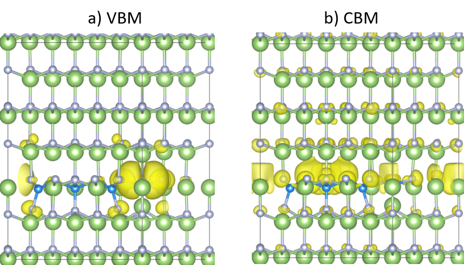
Our discussion above also provides first insight into the configuration with 4 B atoms forming a line in the -plane, which presents such a drastic case in terms of the bandgap reduction: the electronic interaction between - and -like orbitals is enhanced by such an atomic arrangement of B atoms and the interface between BN and GaN in the -plane is increased (and so is the -axis oriented surface area [46]) in comparison to the ”z-line” or 4 B atom ”close” configuration. The expected carrier localization effect in the VBM is confirmed by our DFT calculations, as Fig. 5 shows; interestingly here we also find indications of localization effects in the CBM. Moreover, in this alloy configuration analysis of the bond angles suggests that the B atoms are trying to form a structure resembling hexagonal BN, the ground state crystal structure of BN. This together with our general discussions above may now explain the strong reduction in the bandgap and increased interaction in the -plane of (B,Ga)N containing such a planar arrangement of B atoms.
Conclusion: Overall, our results show that clustering of B atoms in (B,Ga)N alloys, previously observed in experimental studies, may lead to localised states in the valence band, which can cause the bandgap to shrink in the studied B content range of %. These localization effects are introduced by local strain and built-in field effects. Additionally, we find that changes in the bandgap are also tightly linked to local arrangements of B atoms within a cluster: when B atoms form a line in the same -plane, this perturbs the electronic structure and thus the bandgap more significantly when compared to B atoms forming a line along the -axis. In contrast, for alloy configurations where B atoms are distributed throughout the crystal (B atoms not sharing N atoms), the bandgap only changes slightly and localization effects are negligible.
Thus, our investigation of the impact of B atom clustering on the electronic and optical properties of (B,Ga)N alloys highlights the need for controlling the alloy microstructure. If (B,Ga)N is to be used in optoelectronic devices, a film with distributed/separated B atoms may facilitate a structure where (B,Ga)N can be used to lattice-match layers of the heterostructure to reduce strain and consequently also strain-dependent piezoelectric polarization fields. At the same time, the bandgap may only be very slightly affected. As such, if B clustering can be avoided, this may help to improve the efficiency of e.g., UV light emitting devices without affecting the emission wavelengths of the device.
On the other hand, while the introduction of localised states could potentially help to keep carriers away from non-radiative recombination centres (Shockley-Read-Hall recombination), it may also impact radiative and non-radiative (Auger) recombination rates in a non-trivial way as seen for instance in (In,Ga)N quantum well systems [47, 48, 49, 50]. Additionally, our analysis shows that disorder, depending on the alloy atomic configuration, may significantly affect the bandgap. Therefore, designing a device of a particular emission wavelength may be challenging if the alloy microstructure is not controlled. Further experimental and theoretical studies on the electronic, optical and carrier transport properties are now required to understand their consequences for designing optoelectronic devices utilizing this new material system.
This work received funding from the Science Foundation Ireland (Nos. 12/RC/2276 P2 and 21/FFP-A/9014).
References
- [1] Colin J Humphreys “Solid-state lighting” In MRS bulletin 33.4 Cambridge University Press, 2008, pp. 459–470
- [2] H Amano et al. “The 2020 UV emitter roadmap” In J. Phys. D: Appl. Phys. 53.50 IOP Publishing, 2020, pp. 503001
- [3] Pengfei Tian et al. “AlGaN ultraviolet micro-LEDs” In IEEE Journal of Quantum Electronics 58.4 IEEE, 2022, pp. 1–14
- [4] Takashi Mukai, Motokazu Yamada and Shuji Nakamura “Characteristics of InGaN-based UV/blue/green/amber/red light-emitting diodes” In Japanese Journal of Applied Physics 38.7R IOP Publishing, 1999, pp. 3976
- [5] Hideki Hirayama, Sachie Fujikawa and Norihiko Kamata “Recent progress in AlGaN-based deep-UV LEDs” In Electronics and Communications in Japan 98.5 Wiley Online Library, 2015, pp. 1–8
- [6] Max Shatalov et al. “AlGaN deep-ultraviolet light-emitting diodes with external quantum efficiency above 10%” In Applied Physics Express 5.8 IOP Publishing, 2012, pp. 082101
- [7] Burhan K SaifAddin et al. “AlGaN deep-ultraviolet light-emitting diodes grown on SiC substrates” In ACS Photonics 7.3 ACS Publications, 2020, pp. 554–561
- [8] Han-Youl Ryu, Il-Gyun Choi, Hyo-Sik Choi and Jong-In Shim “Investigation of light extraction efficiency in AlGaN deep-ultraviolet light-emitting diodes” In Applied Physics Express 6.6 IOP Publishing, 2013, pp. 062101
- [9] Jong-Il Hwang, Rei Hashimoto, Shinji Saito and Shinya Nunoue “Development of InGaN-based red LED grown on (0001) polar surface” In Applied Physics Express 7.7 IOP Publishing, 2014, pp. 071003
- [10] A Dussaigne et al. “Full InGaN red light emitting diodes” In Journal of Applied Physics 128.13 AIP Publishing LLC, 2020, pp. 135704
- [11] Philip Chan et al. “Demonstration of relaxed InGaN-based red LEDs grown with high active region temperature” In Applied Physics Express 14.10 IOP Publishing, 2021, pp. 101002
- [12] Emmanouil Kioupakis, Patrick Rinke, Kris T Delaney and Chris G Van de Walle “Indirect Auger recombination as a cause of efficiency droop in nitride light-emitting diodes” In Applied Physics Letters 98.16 American Institute of Physics, 2011, pp. 161107
- [13] Robert Kudrawiec and Detlef Hommel “Bandgap engineering in III-nitrides with boron and group V elements: Toward applications in ultraviolet emitters” In Applied Physics Reviews 7.4 AIP Publishing LLC, 2020, pp. 041314
- [14] Thi Huong Ngo et al. “Internal quantum efficiency in yellow-amber light emitting AlGaN-InGaN-GaN heterostructures” In Applied Physics Letters 107.12 AIP Publishing LLC, 2015, pp. 122103
- [15] Logan Williams and Emmanouil Kioupakis “BInGaN alloys nearly lattice-matched to GaN for high-power high-efficiency visible LEDs” In Applied Physics Letters 111.21 AIP Publishing LLC, 2017, pp. 211107
- [16] Brendan P Gunning et al. “Phase degradation in BxGa1-xN films grown at low temperature by metalorganic vapor phase epitaxy” In Journal of Crystal Growth 464 Elsevier, 2017, pp. 190–196
- [17] Logan Williams and Emmanouil Kioupakis “BAlGaN alloys nearly lattice-matched to AlN for efficient UV LEDs” In Applied Physics Letters 115.23 AIP Publishing LLC, 2019, pp. 231103
- [18] J Mickevičius et al. “Type-II band alignment of low-boron-content BGaN/GaN heterostructures” In Journal of Physics D: Applied Physics 52.32 IOP Publishing, 2019, pp. 325105
- [19] Kazushi Ebara et al. “Impact of growth temperature on the structural properties of BGaN films grown by metal-organic vapor phase epitaxy using trimethylboron” In Japanese Journal of Applied Physics 58.SC IOP Publishing, 2019, pp. SC1042
- [20] Richard C Cramer et al. “Growth of coherent BGaN films using BBr3 gas as a boron source in plasma assisted molecular beam epitaxy” In Journal of Vacuum Science & Technology A: Vacuum, Surfaces, and Films 35.4 American Vacuum Society, 2017, pp. 041509
- [21] S Gautier et al. “Deep structural analysis of novel BGaN material layers grown by MOVPE” In Journal of crystal growth 315.1 Elsevier, 2011, pp. 288–291
- [22] Mark E Turiansky, Jimmy-Xuan Shen, Darshana Wickramaratne and Chris G Van de Walle “First-principles study of bandgap bowing in BGaN alloys” In Journal of Applied Physics 126.9 AIP Publishing LLC, 2019, pp. 095706
- [23] Jimmy-Xuan Shen, Mark E Turiansky, Darshana Wickramaratne and Chris G Van de Walle “Thermodynamics of boron incorporation in BGaN” In Physical Review Materials 5.3 APS, 2021, pp. L030401
- [24] Jimmy-Xuan Shen, Darshana Wickramaratne and Chris G Van de Walle “Band bowing and the direct-to-indirect crossover in random BAlN alloys” In Physical Review Materials 1.6 APS, 2017, pp. 065001
- [25] Jochen Heyd, Gustavo E Scuseria and Matthias Ernzerhof “Hybrid functionals based on a screened Coulomb potential” In The Journal of chemical physics 118.18 American Institute of Physics, 2003, pp. 8207–8215
- [26] Aliaksandr V Krukau, Oleg A Vydrov, Artur F Izmaylov and Gustavo E Scuseria “Influence of the exchange screening parameter on the performance of screened hybrid functionals” In The Journal of chemical physics 125.22 American Institute of Physics, 2006, pp. 224106
- [27] Pedro Borlido et al. “Exchange-correlation functionals for band gaps of solids: benchmark, reparametrization and machine learning” In npj Computational Materials 6.1 Nature Publishing Group UK London, 2020, pp. 96
- [28] JP Perdew, ER McMullen and Alex Zunger “Density-functional theory of the correlation energy in atoms and ions: a simple analytic model and a challenge” In Physical Review A 23.6 APS, 1981, pp. 2785
- [29] Yoh Yamamoto et al. “Fermi-Löwdin orbital self-interaction correction using the strongly constrained and appropriately normed meta-GGA functional” In The Journal of chemical physics 151.15 AIP Publishing LLC, 2019, pp. 154105
- [30] Hai Xiao, Jamil Tahir-Kheli and William A Goddard III “Accurate band gaps for semiconductors from density functional theory” In The Journal of Physical Chemistry Letters 2.3 ACS Publications, 2011, pp. 212–217
- [31] John P Perdew et al. “Understanding band gaps of solids in generalized Kohn–Sham theory” In Proceedings of the national academy of sciences 114.11 National Acad Sciences, 2017, pp. 2801–2806
- [32] Stephan Lany and Alex Zunger “Assessment of correction methods for the band-gap problem and for finite-size effects in supercell defect calculations: Case studies for ZnO and GaAs” In Physical Review B 78.23 APS, 2008, pp. 235104
- [33] G. Kresse and J. Furthmuller “Efficient iterative schemes for ab initio total-energy calculations using a plane-wave basis set” In Phys. Rev. B 54.16 ONE PHYSICS ELLIPSE, COLLEGE PK, MD 20740-3844 USA: AMER PHYSICAL SOC, 1996, pp. 11169 DOI: 10.1103/PhysRevB.54.11169
- [34] Koichi Momma and Fujio Izumi “VESTA 3 for three-dimensional visualization of crystal, volumetric and morphology data” In Journal of applied crystallography 44.6 International Union of Crystallography, 2011, pp. 1272–1276
- [35] P. Blochl “Projector augmented-wave method” In Phys. Rev. B 50.24 ONE PHYSICS ELLIPSE, COLLEGE PK, MD 20740-3844 USA: AMER PHYSICAL SOC, 1994, pp. 17953 DOI: 10.1103/PhysRevB.50.17953
- [36] G. Kresse and D. Joubert “From ultrasoft pseudopotentials to the projector augmented-wave method” In Phys. Rev. B 59.3 ONE PHYSICS ELLIPSE, COLLEGE PK, MD 20740-3844 USA: AMER PHYSICAL SOC, 1999, pp. 1758 DOI: 10.1103/PhysRevB.59.1758
- [37] Fabien Tran and Peter Blaha “Accurate band gaps of semiconductors and insulators with a semilocal exchange-correlation potential” In Physical review letters 102.22 APS, 2009, pp. 226401
- [38] Axel D Becke and Erin R Johnson “A simple effective potential for exchange” In The Journal of chemical physics 124.22 American Institute of Physics, 2006, pp. 221101
- [39] J.. Perdew, K. Burke and M. Ernzerhof “Generalized gradient approximation made simple” In Phys. Rev. Lett. 77.18 ONE PHYSICS ELLIPSE, COLLEGE PK, MD 20740-3844 USA: AMERICAN PHYSICAL SOC, 1996, pp. 3865 DOI: 10.1103/PhysRevLett.77.3865
- [40] Cyrus E Dreyer, John L Lyons, Anderson Janotti and Chris G Van de Walle “Band alignments and polarization properties of BN polymorphs” In Applied Physics Express 7.3 IOP Publishing, 2014, pp. 031001
- [41] Thomas P Sheerin and Stefan Schulz “Strain Effects in Wurtzite Boron Nitride: Elastic Constants, Internal Strain, and Deformation Potentials from Hybrid Functional Density Functional Theory” In physica status solidi (RRL)–Rapid Research Letters 16.6 Wiley Online Library, 2022, pp. 2200021
- [42] Atchara Punya and Walter RL Lambrecht “Valence band effective-mass Hamiltonians for the group-III nitrides from quasiparticle self-consistent G W band structures” In Physical Review B 85.19 APS, 2012, pp. 195147
- [43] S. Schulz et al. “Electronic and optical properties of nonpolar a-plane GaN quantum wells” In Physical Review B 82 APS Publishing, 2010, pp. 125318
- [44] F. Bernardini, V. Fiorentini and D. Vanderbilt “Spontaneous polarization and piezoelectric constants of III-V nitrides” In Physical Review B 56, 1997, pp. R10024
- [45] Miguel A Caro, Stefan Schulz and Eoin P O’Reilly “Theory of local electric polarization and its relation to internal strain: Impact on polarization potential and electronic properties of group-III nitrides” In Physical Review B 88.21 APS, 2013, pp. 214103
- [46] S Schulz and E.. O’Reilly “Theory of reduced built-in polarization field in nitride-based quantum dots” In Physical Review B 82 APS Publishing, 2010, pp. 033411
- [47] C.. Jones et al. “Impact of carrier localization on recombination in InGaN quantum wells and the efficiency of nitride light-emitting diodes: Insights from theory and numerical simulations” In Appl. Phys. Lett. 111, 2017, pp. 113501
- [48] J.. McMahon, E. Kioupakis and S. Schulz “Atomistic analysis of Auger recombination in -plane (In,Ga)N/GaN quantum wells: Temperature dependent competition between radiative and non-radiative recombination” In Phys. Rev. B 105, 2022, pp. 195307
- [49] J.. McMahon, E. Kioupakis and S. Schulz “Erratum: Atomistic analysis of Auger recombination in -plane (In,Ga)N/GaN quantum wells: Temperature dependent competition between radiative and non-radiative recombination” In Phys. Rev. B 108, 2023, pp. 039901(E)
- [50] R.. Barrett et al. “Disentangling the Impact of Point Defect Density and Carrier Localization-Enhanced Auger Recombination on Efficiency Droop in (In,Ga)N/GaN Quantum Wells” In ACS Photonics in press, 2023, pp. https://doi.org/10.1021/acsphotonics.3c00355
See pages - of BGaN_SI.pdf