These two authors contributed equally.††thanks: siwakiri@phys.ethz.ch; amestre@phys.ethz.ch;
These two authors contributed equally.
Tunable quantum interferometer for correlated moiré electrons
Abstract
Magic-angle twisted bilayer graphene (MATBG) can host an intriguing variety of gate-tunable correlated states, including superconducting and correlated insulator states. Junction-based superconducting devices, such as Josephson junctions and SQUIDs, have been introduced recently and enable the exploration of the charge, spin, and orbital nature of superconductivity and the coherence of moiré electrons in MATBG. However, complementary fundamental coherence effects — in particular, the Little–Parks effect in a superconducting and the Aharonov–Bohm effect in a normal conducting ring — remained to be observed. Here, we report the observation of both these phenomena in a single gate-defined ring device where we can embed a superconducting or normal conducting ring in a correlated or band insulator. We directly observe the Little–Parks effect in the superconducting phase diagram as a function of density and magnetic field, confirming the effective charge of . By measuring the Aharonov–Bohm effect, we find that in our device, the coherence length of normal conducting moiré electrons exceeds a few microns at 50 mK. Surprisingly, we also identify a regime characterized by -periodic oscillations but with superconductor-like nonlinear transport. Taken together, these experiments establish a novel device platform in MATBG, and more generally in tunable 2D materials, to unravel the nature of superconductivity and other correlated quantum states in these materials.
Magic-angle twisted bilayer graphene (MATBG) with its moiré flat band Suárez Morell et al. (2010); Zhang et al. (2019) constitutes a condensed-matter system to realize a wide variety of correlated states, such as superconducting and correlated insulator states, that are tunable by gating Cao et al. (2018a, b); Yankowitz et al. (2019); Lu et al. (2019, 2019); Saito et al. (2020); Stepanov et al. (2020); Di Battista et al. (2022). A novel class of gate-defined nanodevices, including Josephson junctions de Vries et al. (2021); Rodan-Legrain et al. (2021) and SQUIDs Portolés et al. (2022), have been recently realized in MATBG. These structures have provided excellent platforms for controlling mesoscopic superconductivity and characterizing MATBG. Extending this approach to a doubly-connected geometry without any junction, namely a ring, promises unique microscopic information about the material and the device.
The physical properties of a ring threaded by a magnetic field are in general periodic in flux quanta Byers and Yang (1961); Bloch (1970) , with being the charge of the carrier. In a superconducting ring (), -periodic oscillations of critical temperature and critical current appear. These oscillations are known as the Little–Parks effect and were the first experimental evidence for the charge pairing in conventional superconductors Little and Parks (1962); Groff and Parks (1968). In fact, the Little–Parks effect can be used to determine the charge of the superconducting carriersBalents et al. (2020); Yang et al. (2023), complementing the Josephson-junction and SQUID experimentsde Vries et al. (2021); Portolés et al. (2022). Moreover, properties of unconventional superconductors can be revealed by anomalies of the Little–Parks effect, such as a phase shift Liu et al. (2018); Hua et al. (2022); Aoyama (2022); Geshkenbein et al. (1987); Xu et al. (2020); Li et al. (2019); Almoalem et al. (2022) or a change in periodicity Loder et al. (2008); Juričić et al. (2008); Zhu and Quan (2010); Fernandes and Fu (2021); Jiang et al. (2017); Almoalem et al. (2022), and thereby help to understand the underlying superconducting symmetry.
By contrast, a normal conducting ring () shows -periodic oscillations of resistance, the Aharonov–Bohm effect, and works as a direct probe to quantify the phase coherence of electrons. Given the low Fermi velocity and the large effective mass in MATBG, a possible non-Fermi liquid nature of its flat band electrons Cao et al. (2018b, 2020), and intrinsic disorders introduced by twist-angle inhomogeneity Uri et al. (2020), quantifying the phase coherence length is key to understanding the dynamics of moiré electrons. In addition, the phase coherence length enables the estimation of the penetration depth of a superconducting wave function into the normal conducting state (proximity effect) de Gennes (1964); Clarke (1968), which plays an important role in gate-defined superconducting devices. However, the exploration of these fundamental quantum interference effects has been hampered by the lack of a suitable device architecture and the sensitivity of the moiré superlattice to disorder Uri et al. (2020), which poses a challenge to the conventional approach of fabricating a ring by physical/chemical etching.
Here we present such an architecture with a gate-defined ring consisting of a loop that can be tuned to be superconducting or normal conducting, surrounded by a correlated or band insulator. We confirm pairing via the Little–Parks effect, and show that the phase coherence length of moiré electrons surpasses several microns at 50 mK, evidenced by -periodic Aharonov–Bohm oscillations. We also discover an intriguing regime in which -periodic oscillations appear alongside superconductor-like transport. These results highlight the promise of the novel quantum interferometer in MATBG for studying interference phenomena of exotic quantum states of 2D materials.
Highly tunable quantum interference
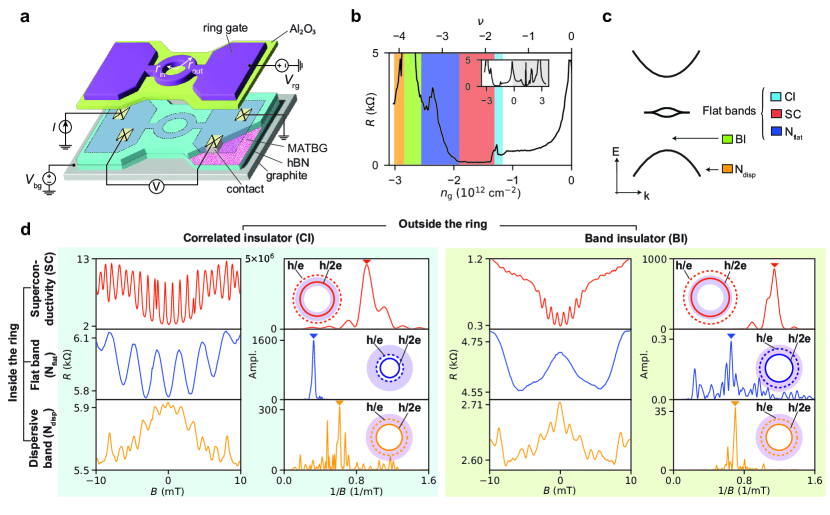
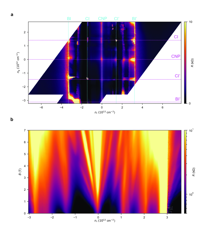
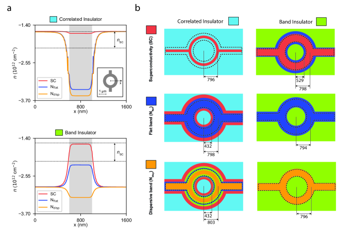
We develop the gate-defined ring architecture shown in Fig. 1a. We base the design on the proof-of-principle device reported in ref. Iwakiri et al. (2022) using Bernal bilayer graphene. The MATBG is encapsulated in hexagonal boron nitride (hBN) and is contacted by four electrodes. The sample is dual-gated with a graphite back gate and a metallic ring-shaped top gate (ring gate). We operate the ring by first tuning the back gate voltage , which affects the entire MATBG area and induces a global density . Then we tune the density under the ring gate, , via the voltage . The ring has a lithographic inner radius of and an outer radius of . Through the electrodes, the sample is biased with a current , and the voltage drop is measured in a four-terminal configuration. Unless stated otherwise, the measurements are performed in a 3He–4He dilution refrigerator at a temperature of .
The resistance of the MATBG (Fig. 1b) as a function of with set to zero shows pronounced peaks at charge neutrality, and in the correlated insulator (CI) and band insulator (BI) regimes on the hole side (). From the density at the BI peak, we estimate an average twist angle of . When tuning the density beyond the correlated insulator, we observe superconductivity (SC) through a resistance drop. We also access two normal conducting regimes: one inside the flat band (N) and the other in the dispersive band (N). Figure 1c summarizes the relevant quantum states that form in the device. Further details of the experimental setup are given in the Methods and Extended Data sections.
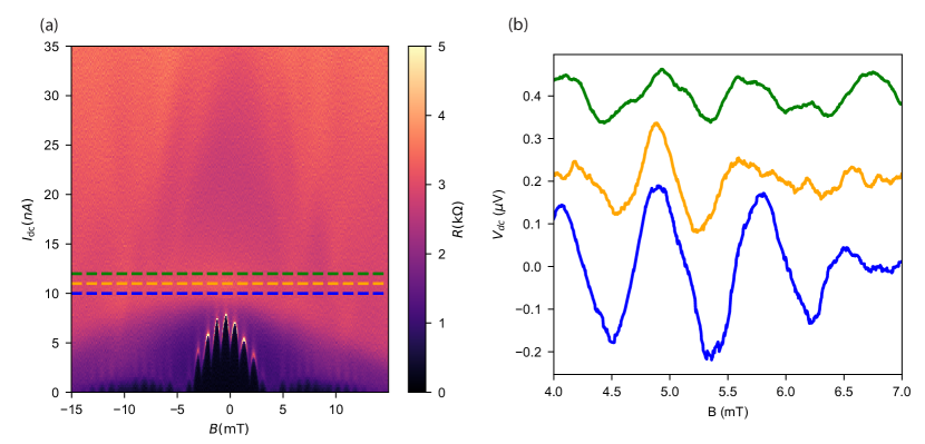
In order to define a conducting path, we tune the ring-shaped region into the SC, N, or N regimes. This conducting path is then surrounded by either CI or BI states to confine electrons. As we will see below, the insulating state does not influence the observed interference pattern but has an effect on the quantum state distribution across the structure (see Supplementary Information 8). Figure 1d shows the resistance () oscillations in perpendicular magnetic field () for the six regimes at zero bias current and a temperature of 150 mK, together with their fast Fourier transform (FFT) spectra. When calculating the FFT spectrum, we subtract a smooth background extracted with the Savitzky–Golay filter. We convert the peak of the spectrum into an area assuming either or -periodicity as the relevant flux quantum and then compare the result with the lithographic radius of the ring (see inset circles in Fig. 1d).
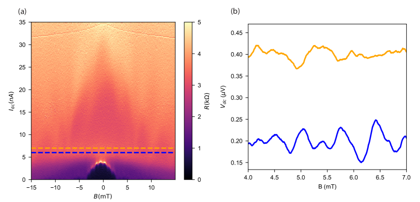
In the case of a superconducting ring (top row in Fig. 1d, ), the frequency peak appears at 0.92/mT for (SC, CI) and at 1.20/mT for (SC, BI). Hereafter, we denote the state inside and outside the ring as (inside, outside). Assuming -periodicity, the observed frequency peaks correspond to an effective radius of and , respectively. These values are comparable to the center-line radius of the ring gate . In contrast, the when assuming -periodicity does not match the lithographic dimension of the ring gate (). In these regimes, we further observe critical current and critical density oscillations, as we discuss in Fig. 2. Based on our findings, we attribute these oscillations to the -periodic Little–Parks effect, confirming that the charge of the superconducting carrier is .
When the ring is tuned into the dispersive band (bottom row in Fig. 1d, ), -periodic oscillations appear with a spectrum covering a significant range in . The peak frequency of the oscillations is 0.621/mT for both (N, CI) and (N, BI). This frequency is approximately half of those observed in the superconducting case, suggesting an -periodicity. The effective radii both assuming - () and -periodicity () fit within the ring dimensions. However, the oscillation amplitude decays exponentially in temperature and strives at higher magnetic fields than the Little–Parks oscillations (see Supplementary Information 2). The amplitude decay in temperature is characteristic of the Aharonov–Bohm oscillations due to the smearing of the Fermi function and the reduction of the phase coherence length Hansen et al. (2001). We therefore attribute the oscillations to the -periodic Aharonov–Bohm effect. The measurement of the temperature dependence also allows us to estimate the phase coherence length of electrons in the dispersive band (see Supplementary Information 2). At 50 mK, the coherence length is in (N, CI) and in (N, BI). These values exceed the perimeter of the ring (). This result demonstrates that the phase coherence of moiré electrons in the dispersive band is well preserved despite several sources of disorder such as twist-angle inhomogeneity and strain distribution.
Furthermore, there is a striking contrast between the oscillation in the normal conducting flat band regimes depending on the surrounding insulators (middle row in Fig. 1d, ). In the (N, CI) regime, we observe an oscillation with a frequency of 0.630/mT, even lower than in the SC and N cases. The effective radius assuming periodicity is , even smaller than , while for -periodicity matches . Though the geometric argument points towards -periodicity, this regime exhibits superconductor-like transport as well. We discuss this point in more detail later in Fig. 3. On the other hand, in the (N, BI) regime, we observe magneto-resistance oscillations with very small amplitude. In this regime, the frequency peak appears close to the one in the regime. The effective radius is assuming -periodicity and assuming -periodicity. This regime shows neither nonlinear transport nor a drop in resistance with temperature. Therefore, we attribute the oscillations in the (N, BI) regime to -periodic Aharonov–Bohm oscillations. The phase coherence length, estimated from the temperature dependence, is , which is by a factor of 2–3 smaller than that for N. This relatively short in the flat band can be attributed to a large electron effective mass. In fact, the phase coherence length is proportional to the Fermi velocity , which depends inversely on the effective mass (), and the measured in the flat and dispersive bands are different by a factor of 1–10.Cao et al. (2018b)
These results demonstrate that one can switch between the Little–Parks and the Aharonov–Bohm effects of MATBG by gate tuning. They also reveal the charge pairing and long coherence lengths of the moiré electrons. In the following sections, we discuss each regime in more detail.
Tunable Little–Parks oscillations
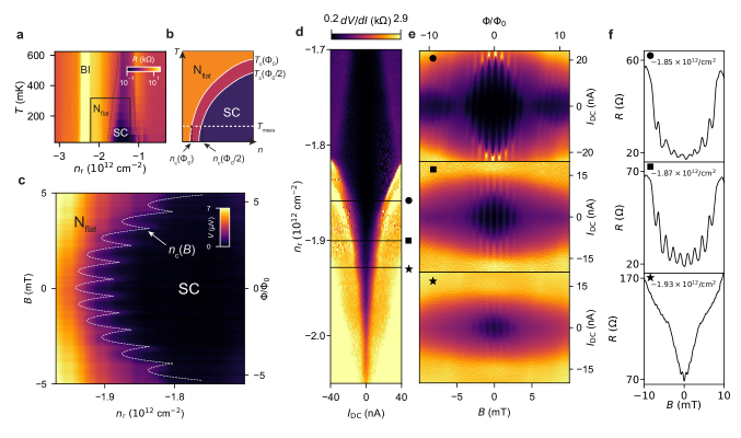
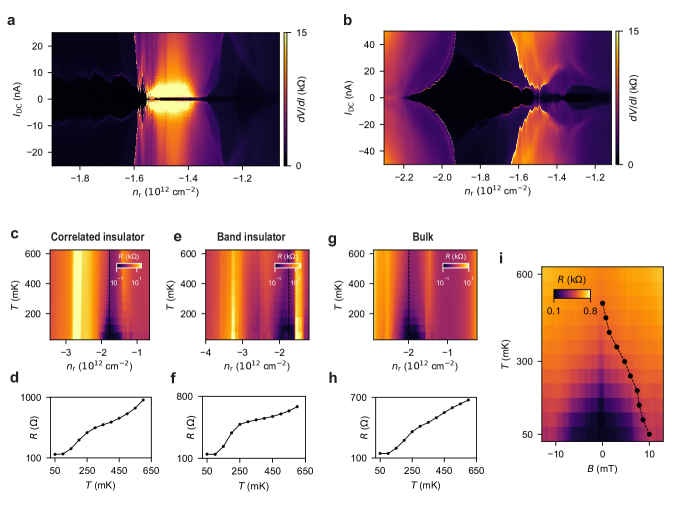
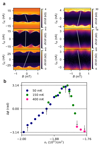
The Little–Parks effect is essentially the magneto-oscillation of the free energy of the superconducting stateTinkham (2004), which results in the oscillation of the critical temperature and the critical current . While the critical current is readily measurable, the current injection inevitably drives the system out of equilibrium, possibly giving rise to unwanted effects such as local breakdown of superconductivity Fink et al. (1987, 1988); Moshchalkov et al. (1993). Therefore, a measurement at equilibrium is preferable. Besides, measurement of the oscillation is experimentally challenging as the expected amplitude is in the sub-mK range Tinkham (2004). Here, taking advantage of the in-situ tunability of the carrier density in MATBG, we demonstrate an alternative route to detect Little–Parks oscillations. We probe the oscillation of by translating it into the oscillation of the critical density at which the superconducting transition occurs, enabling the detection of the Little–Parks effect near equlibrium. Figure 2a shows the phase diagram of the device in the (SC, BI) regime, measuring the resistance as a function of temperature and at zero magnetic field. Increasing the temperature from 50 mK to 600 mK, the density range of the SC state shrinks, forming a superconducting dome. Due to the Little–Parks effect, the of the superconducting ring oscillates with the magnetic flux. As depicted in Fig. 2b, this results in a compression and expansion of the superconducting phase boundary. For a fixed temperature , such breathing can be translated into an oscillation of the critical density , between and . It is therefore possible to probe the magneto-oscillation of the phase boundary by fixing the temperature and sweeping the carrier density.
Figure 2c shows the measured voltage drop across the ring as a function of and , at a DC bias current of and in a density range close to the high-density edge of the superconducting dome (see Supplementary Information 10 for the temperature and current dependence of the map). At a fixed , a jump from zero to a finite voltage marks the transition from the superconducting to the normal conducting regime. The magnetic field dependence of the density represents the phase boundary. At , is the maximum in absolute value. The shape of this boundary oscillates with a period of 0.870 mT, agreeing with an -periodicity (). The smooth shift of the phase boundary with increasing to higher electron densities reflects the shrinking of the superconducting dome in . We observe the same result with a reversed current (). All in all, this means that MATBG exhibits a conventional Little–Parks effect, unlike the shifted pattern observed in some unconventional superconductors Liu et al. (2018); Almoalem et al. (2022). The demonstration of the Little–Parks effect near equilibrium by constructing the phase diagram is one of the distinct advantages of the gate-defined architecture.
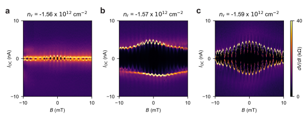
We can also track the development of the oscillations as the state departs from the vicinity of the SC-to-N transition into deep inside the superconducting dome by tuning the density . Fig. 2d shows as a function of DC current and at zero magnetic field, and Fig. 2e the - and -dependence of for (see solid horizontal lines in Fig. 2d). The periodic oscillations of the critical current emerge on top of a decreasing background in magnetic field. The periodicity of the oscillations is (0.87 mT), in agreement with the (SC, BI) data in Fig. 1d. As is tuned to a value that shows larger (deep inside the superconducting dome), the amplitude of the oscillations increases and they are also observed up to higher magnetic fields. Moreover, the magnetic field origin of the oscillations shifts from zero and also depends on the direction of the applied current (see Fig. Supplementary Information 9), which can be due to the inductance of the ring. At the lowest density (Fig. 2e, top panel), we observe that the critical current vanishes at mT and re-emerges at a higher magnetic field. This pattern resembles the Fraunhofer pattern of Josephson junctions. However, as we discuss in the Supplementary Information section, the width of this hypothetical Josephson junction does not fit any of our ring geometries. We therefore attribute the observed pattern rather to the existence of multiple interference paths within the ring, generating a beating pattern.
The differential resistance traces at zero bias current ( nA) for the three densities are shown in Fig. 2f. Close to the SC-to-N transition (bottom panel, star symbol), the magneto-resistance oscillations are barely visible as the difference of resistance between SC and the normal states is vanishing. When the density is increased (middle panel, square symbol), we observe pronounced oscillations where a chain of parabolas appears on top of a smooth parabolic background. When the density is further increased (top panel, circle symbol), the oscillation amplitude drops again. This is because the state is deep in the superconducting dome and zero current is too remote from the transition to fully capture the Little–Parks effect. As a matter of fact, deeper in the superconducting dome, one can only observe the critical current oscillations.
Spectroscopy of the quantum oscillations
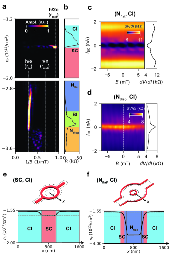
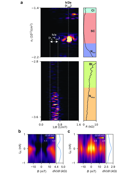
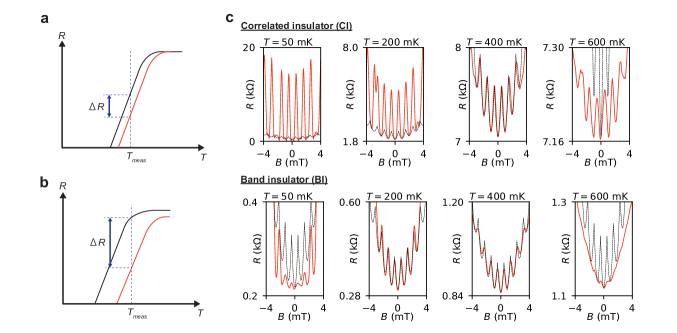
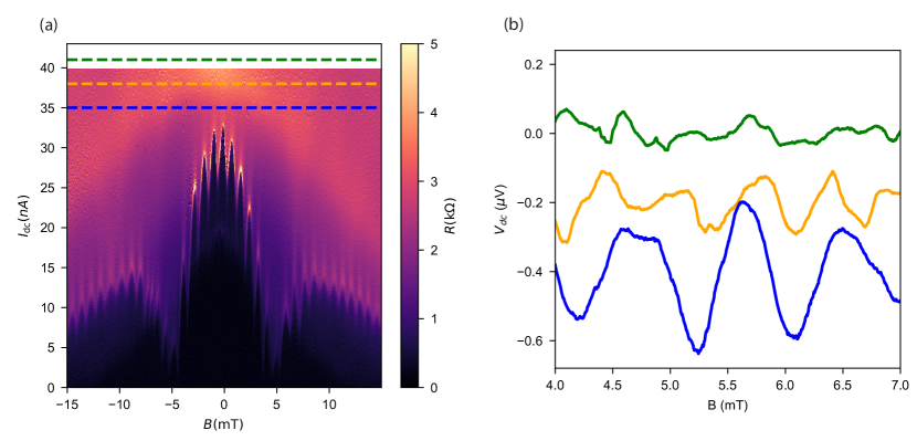
Figure 3a shows the magneto-oscillation spectrogram as a function of the density when the state outside the ring is CI (see Fig. 1d, left column). The spectrogram is constructed by first measuring the differential resistance at zero bias current sweeping the magnetic field between 20 mT. Then the FFT spectrum is calculated after subtracting the smooth background from the raw data. In the spectrogram, we observe several regions with prominent peaks in the FFT. The resistance at zero magnetic field and corresponding quantum states are shown in Fig. 3b.
An peak is observed () at the edge of the SC region in the vicinity of the CI regime. This can be understood by the fact that the Little–Parks oscillation only appears at the onset of the superconducting transition. When the density is tuned further down to the (, CI) regime, a prominent peak at 0.313 /mT appears between . This corresponds to an effective radius of assuming -periodicity, and assuming . As the latter is considerably smaller than , we attribute an -periodicity to the oscillations. The density window across which this peak extends is unexpectedly wide and includes the BI regime, meaning that the oscillations persist even when the ring is mostly insulating. When entering the (N, CI) regime, the spectrum becomes broader and features a peak within the -periodic range (). This broad spectrum is not unexpected for conventional Aharonov–Bohm oscillations as the aspect ratio of the gate-defined ring is small (), making possible many interference paths with different effective enclosed areas. The oscillations in (N, CI) and in (N, CI) not only differ in peak frequency and frequency extent but also show different responses to . Figure 3c,d show the and mapping in (N, CI), with cm-2, and (N, CI), with cm-2 respectively. Interestingly, a superconductor-like behaviour of the differential resistance (dip at nA) is observed in the (N, CI) regime, despite the high resistance reaching up to a few k. In addition, a periodic chain of low-resistance states appears by sweeping and . By contrast, the (N, CI) regime exhibits a cusp in differential resistance at nA, and no characteristic pattern is observed in the and mapping. This again supports the interpretation that Aharonov–Bohm oscillations are observed for (N, CI).
We attribute the superconducting behaviour of the (N, CI) regime to the presence of a small residual superconducting region, emerging from the smooth evolution of the carrier density from inside to outside of the ring. To support this idea, we perform an electrostatic simulation of the carrier density distribution (see Supplementary Information). As shown in Fig. 3e, in (SC, CI) regime, SC is the only state inside the ring. However, when the ring is detuned from the (SC, CI) to the (N, CI) regime (Fig. 3f), the spatial distribution of the quantum states becomes complex and a superconducting region can be embedded around the ring. This spurious superconducting region consists of a small ring with radius and a path surrounding the gated region, as the schematics of Fig. 3f depicts.
Further improvement of the simulation, taking the proximity effect at the interface of different quantum states into account, can help to understand this regime better.
Conclusion
In conclusion, we present a gate-defined quantum interferometer in MATBG that provides a versatile platform for investigating the quantum coherence and the charge of correlated electrons from superconducting to normal conducting regimes. We observe the Little–Parks effect by constructing the superconducting phase diagram as well as by measuring the oscillation of the magneto-resistance and critical current, confirming the charge- pairing. We also observe the Aharonov–Bohm effect for the dispersive and flat band electrons in the same device. From it, we extract the phase coherence length exceeding a few microns, highlighting the robustness of its phase coherence. We find a regime that exhibits magneto-resistance and critical current oscillations even detuned from the superconducting regime, which might be due to the electrostatic constriction of the device.
These experiments demonstrate that exploring the Little–Parks effect has the potential to provide insight into both the charge and spin nature of the Cooper pair in MATBG. Notably, the measurement under an in-plane magnetic field along with the perpendicular field could enable the observation of phase shifts in Little–Parks oscillations. Such shifts could serve as indicators of unconventional pairings such as spin-triplet superconductivityAoyama (2022); Yasui et al. (2017); Jang et al. (2011). Moreover, the gate-defined architecture and the measurement scheme presented here can generally be implemented in other 2D superconductors (e.g., twisted multilayer grapheneCao et al. (2021), Bernal bilayer grapheneZhou et al. (2022), and bilayer graphene/transition metal dichalcogenideZhang et al. (2023)), opening up the path towards the direct quantification of charge, spin, and coherence of correlated electrons in a plethora of exotic quantum states.
Acknowledgements.
We thank Peter Märki, Thomas Bähler, and the staff of the ETH cleanroom facility FIRST for technical support. We thank Lev Ginzburg and Rebekka Garrais for their help with the experiments. We thank Andreas Trabesinger for his valuable input during the writing process of this manuscript. We acknowledge financial support by the European Graphene Flagship Core3 Project, H2020 European Research Council (ERC) Synergy Grant under Grant Agreement 951541, the European Union’s Horizon 2020 research and innovation program under grant agreement number 862660/QUANTUM E LEAPS, the European Innovation Council under grant agreement number 101046231/FantastiCOF, NCCR QSIT (Swiss National Science Foundation, grant number 51NF40-185902). K.W. and T.T. acknowledge support from the JSPS KAKENHI (Grant Numbers 21H05233 and 23H02052) and World Premier International Research Center Initiative (WPI), MEXT, Japan. E.P. acknowledges support of a fellowship from ”la Caixa” Foundation (ID 100010434) under fellowship code LCF/BQ/EU19/11710062.I Supplementary Information
I.1 Measurement setup
We carry out all the measurements in a dilution refrigerator that uses a mixture of 3He and 4He with a base temperature of . We apply a constant current bias between a pair of contacts across the ring and measure the voltage drop between another pair, also across the ring. To generate the bias current, we use an in-house-built d.c. source in series with a resistor. We use a d.c. amplifier, also built in-house, and measure its output with a Hewlett Packard 3441A digital multimeter. Each gate is connected to a different voltage source of the same type as the one used for generating a d.c. current. We convert the voltages we apply to the gates to electron densities by a parallel plate capacitor model. We estimate the capacitance per unit area of the back and ring (top) gate to be and , where is the vacuum permittivity, and are the relative permittivities of the hBN and the aluminium oxide, and are the thicknesses of the top and bottom hBN and is the thickness of the aluminium oxide layer. We calculate the electron density of the bulk as and of the region below the top gate as , where is the elementary charge.
I.2 Twist angle estimation
We extract the twist angle of the sample using the relation Cao et al. (2018a). In this expression, is the lattice constant of graphene and is the moiré periodicity, which represents the distance between two adjacent AA-stacked regions. In turn, is related to the area of the moiré unit cell via . Within a moiré unit cell, four electrons can be accommodated due to spin and valley degeneracy. Then, the band insulator peak due to the twist appears at the electron density which corresponds to the occupation of 4 electrons per moiré unit cell . We obtain from the Landau fan and density mapping (Supplementary Information 11). Our analysis yields to an approximate twist angle of .
I.3 Device fabrication
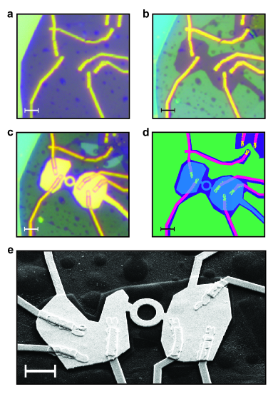
The device stack is assembled using the dry pick-up method Kim et al. (2016). We exfoliate graphene and hexagonal boron nitride (hBN) flakes on a wafer. We start by scratching a graphene flake in two using a tungsten needle with a tip diameter of controlled by a micromanipulator. We pick up all the flakes using a polydimethylsiloxane/polycarbonate stamp. We first pick up the top hBN flake, with a thickness of , at . Then we proceed to pick up the graphene and assemble the twisted structure. For this, we first pick up half of the pre-cut graphene, rotate the microscope stage by and then pick up the other half of the graphene, all at . We encapsulate the graphene by picking up a bottom hBN flake, with a thickness of . For the encapsulation, the stack is first contacted to the bottom hBN at and the temperature of the stage is raised to . Finally, we pick up a graphite flake of at that serves as a back gate. The stack is then deposited at on a chip. After deposition, we clean the polycarbonate stamp using dichloromethane.
We contact the MATBG with edge contacts made by electron beam lithography followed by reactive ion etching, using (40/4 sccm, 60W). The contacts are then evaporated using Cr/Au (10/80 nm). We define the electrode lines in two steps using electron beam lithography and depositing Cr/Au (10/60 nm for the first step and 5/50 nm for the second). Then we etch the stack to define the mesa and deposit a thick layer of aluminium oxide by atomic layer deposition. For the ring-shaped top gate, we again use electron beam lithography and evaporate Cr/Au (5/35 nm). The electrode line for the top gate is also done by electron beam lithography and evaporation using Cr/Au (10/70 nm).
I.4 Optical images and design of the sample
I.5 Raw data for magneto-resistance

I.6 Density maps and angle extraction
I.7 Critical density oscillations at different DC-bias currents and temperatures

I.8 Critical current oscillations in the CI regime
I.9 Critical current, critical field and critical temperature
I.10 Spectrogram of quantum oscillations in the BI regime
I.11 Electrostatic simulation
We perform electrostatic simulations of the carrier density distribution in the MATBG ring presented in this work. The inset in the top panel of Fig. Supplementary Information 8a shows a top view of the geometry of the structure. In the simulations, we discretize the system with a finite element model and self-consistently solve the Poisson equation () using the software COMSOL Multiphysics. In the equation, is vacuum permittivity, is relative permittivity of the dielectric layer ((hBN) = 3.3 and (AlOx) = 9.5), is electric potential at position x, and is the charge density at position x. We impose in the dielectric layers and implement in the MATBG plane using the Thomas-Fermi approximation Luscombe et al. (1992). We simplify the band structure of MATBG assuming parabolic bands for both the flat and the dispersive bands, with respective effective masses and Cao et al. (2018b); Rodan-Legrain et al. (2021). We assume a band gap of 30 meV for the BI state, separating the flat and dispersive bands Rodan-Legrain et al. (2021). We impose on the top side of the top hBN layer and at the bottom of the bottom hBN layer. We approximate the CI state with a smaller energy gap of 0.3 meV. After solving Poisson’s equation, the carrier density is directly extracted from the calculated surface charge density using .
The simulated carrier density distributions along the horizontal cut across the arm of the ring are shown in Fig. Supplementary Information 8a. The left and right panels correspond, respectively, to the regimes in which the outside of the ring is in the CI ( V) and BI regime ( V). In both panels, we show the charge distribution when the ring is set to the superconducting state ( when CI outside and when BI outside), normal conducting in the flat band ( when CI outside and when BI outside) and in the dispersive band ( when CI outside and when BI outside). The vertical dashed lines indicate the lithographic width of the ring (400 nm), while the horizontal lines show the density range of the superconducting state. For all six conditions, the fringing field results in a broadening of the carrier density distribution, making the actual width of the targeted quantum state wider/smaller than the lithographic width of the ring gate. Fig. Supplementary Information 8b shows the carrier density distribution in the MATBG layer for the six configurations. Because the quantum states in MATBG are density-dependent, the broadening of the carrier density distribution leads to a stripe structure of phases across the sample. The insets in Fig. Supplementary Information 8b. show the quantum state distribution across the arm of the ring. The charge densities at which each quantum state (CI, SC, Nflat) arises are extracted from the map in Fig. Supplementary Information 11a. Owing to the circular symmetry of the system, multiple quantum state stripes form a ring with different radii and could contribute to oscillations.
Even in (N, CI) regime, a superconducting path can be formed. In particular, there is a small superconducting ring with a radius of 432 nm and an open path surrounding the outer edge of the N region. Such a spurious superconducting path could contribute to the transport characteristics such as the one observed in Fig. 3. Moreover, the oscillations in resistance and critical current observed in the (N, CI) regime have a period of 3.19 mT, corresponding to an effective radius of 446 nm in . This number coincides with the small superconducting ring predicted by the simulation, though more work is necessary to confirm the existence of such a ring by taking the superconducting proximity effect into account.
Such a satellite superconducting path is also predicted in (N, CI) regime, where only the conventional Aharonov–Bohm effect ( in between and ) and no superconducting-like nonlinearity are experimentally observed. In this regime, there is a BI state between the N state and the satellite superconducting path, which might make the majority of the current flow away from the superconducting path.
I.12 Tunable phase shift of the Little–Parks effect
The magnetic field at which the critical current reaches its maximum () depends on the sign of the current, as can be seen in Fig. Supplementary Information 9a. This means that there is a phase shift in the magneto-oscillation of the critical current depending on the polarity of the bias current. Here, we show that the ring gate tunes this phase shift. To characterize this phase shift, we extract and convert it to a phase shift in flux . As shown in Fig. Supplementary Information 9.b, monotonically decreases from to and vanishes when .
Such an asymmetry can be attributed to the slight shape-asymmetry of the superconducting path inside the ring, which is presumably gate-dependent. It could result in a difference in the inductance of each arm.
Our observations imply that special care has to be taken when analyzing the phase of the Little–Parks oscillations in critical current in a thin superconductors, as the large inductance of the material can result in an inevitable phase shift.
I.13 Interpretation of the temperature dependence of the Little–Parks effect
The Little–Parks effect is usually measured as a magneto-resistance oscillation and then converted to an oscillation of the critical temperature. There, a translation of is used (see Fig. Supplementary Information 10(a). Here, and are the amplitude of the magneto oscillation of the resistance and the critical temperature, respectively. Tinkham derived the theoretical formula for , where is the critical temperature at zero magnetic field, is the BCS coherence length, and an integer number. Here, it is assumed that the shape of the temperature dependence of the resistance does not change with the magnetic field, making constant in a wide range of temperature as shown in Supplementary Information 10(a).
However, as shown in Fig. Supplementary Information 10, the Little–Parks effect observed here strongly depends on the temperature. In addition, as we show here, fitting the magneto-resistance data to Tinkham’s formula is valid in a limited range of temperatures even though the observed amplitude of is larger than the expected value by a factor of ten. Such discrepancies could arise from the breakdown of the assumption that the shape of the temperature dependence of the resistance does not change with the magnetic field. In 2D superconductors such as MATBG, the thickness is always shorter than the penetration length of the magnetic field (Pearl length), letting magnetic flux always penetrate as soon as the magnetic field is applied. Therefore, the critical temperature is modulated not only by the Little–Parks effect but with the magnetic field itself, making Tinkham’s assumption break.
Also, we discuss that the observation of the Little–Parks effect prefers a temperature that is close enough to the critical temperature. The condensation energy of a superconductor with a width , thickness and length is . Here, is vacuum permeability, and is the Ginzburg-Landau coherence length with being the zero-temperature coherence length. Then, sets an approximate condition that such a piece of superconductor becomes unstable. At a fixed temperature , the maximum length of such a broken area is
| (S1) |
Then, if , the superconductor hosts a piece of normal conducting part, which does not extend across the entire ring. Such a part would make a Josephson junction in the system. Equation S1 leads to the condition that
| (S2) |
Equation S2 predicts a characteristic temperature at which the non-superconducting regime extends the entire ring. is analytically obtained
| (S3) |
Here, . It can be seen that is very close to . For example, if nm, nm, nm, nm, and mK, mK. Though the above calculation is a crude estimation, it is suggested that the ring becomes more homogeneous as the temperature increases close to the critical temperature. This supports that the observed asymmetry in the Little–Parks oscillations becomes less prominent at higher temperatures and with a density where the superconducting state has a small critical current.
I.14 Interpretation of the beating pattern
As shown in Fig 2, the critical current reaches zero at in the (SC, BI) regime. One explanation of such an effect is the formation of a spurious Josephson junction in the system, that would produce a Fraunhofer-like pattern. However, this hypothesis fails to explain the observed data quantitatively. Namely, for a 2D planar Josephson junction Clem (2010); Fermin et al. (2023), the magnetic field at which the critical current vanishes is , where is the lateral width of the junction. Using this formula, the magnetic field of is converted to an effective junction width of . This dimension significantly exceeds the width of the arm of the ring (400 nm), inferring that the superconductivity inside the ring is homogeneous and does not host any junction.
Another possibility that could explain the vanishing critical current is the existence and interference of multiple superconducting paths inside the ring. In fact, the central frequency of the Little–Parks oscillation (1.1/mT) coincides with the center radius of the ring (855 nm). If superconducting paths with effective radii of 87 nm (frequency 0.8/mT) or 650 nm (frequency 1.2/mT) are also present, their interference would produce a beating frequency of 0.2/mT that equals to the beating periodicity of 5 mT.
I.15 Distinguishing Little–Parks effect from SQUID
Due to the fluxoid quantization in superconductors Tinkham (2004), when a magnetic field is applied perpendicular to the device plane, there will be a circulating current around any hole threaded by the field. If that current flows in a region of the superconductor that has a nonzero resistance this will lead to the so-called Little–Parks effect Little and Parks (1962); Groff and Parks (1968). In the case of 3D superconductors, current flows through the bulk, without encountering any resistance. However, for two-dimensional materials, where the penetration depth of the magnetic field is bigger than the thickness of the material, the whole superconducting surface has nonzero resistance. The Little–Parks effect is thus expected in any two-dimensional superconducting device.
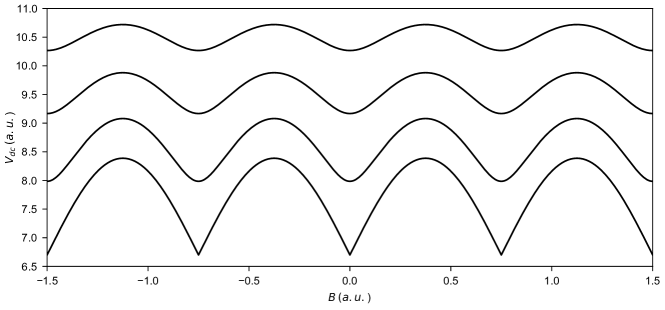
The question that remains in the case of a two-dimensional ring is whether there can be spontaneous formation of Josephson junctions leading to a SQUID-like behaviour. To discern between the two behaviours, we focus on the oscillations in voltage drop across the device when biased above the critical current. There, oscillations in the voltage drop are expected both in the Little–Parks and SQUID cases. In the former, they are expected due to the finite breadth in current of the superconducting transition. In the case of the latter, the oscillations are expected due to the fact that even if the junctions present in the ring are biased above their critical currents, the superconducting condensate in the rest of the ring is still present and thus superconducting coherence and subsequent interference phenomena still take place Clarke and Braginski (2006).
The difference between the two types of oscillations is that for the SQUID ones a particular shape is expected while the ones stemming from Little–Parks effect are not expected to take any particular shape. For the ones originating from SQUID behaviour, the following voltage dependence is expected in the case of two overdamped junctions:
| (S4) |
where is the resistance of the two Josephson junctions in parallel, the flux threading the loop, and the superconducting flux quantum. Assuming that the eventual junctions that form in the material are overdamped is reasonable taking into account the low critical currents and quasiparticle resistances expected in junctions in this material, from measurements performed in devices with electrostatically engineered junctions Portolés et al. (2022). Figure Supplementary Information 11 shows the expected voltage drop for such a case. Figures Supplementary Information 12-Supplementary Information 14 show the corresponding line plots taken at different current biases when sweeping the magnetic field. We observe no particular resemblance between the data and the expected trend. As a comparison, we performed the same analysis for a SQUID device in this material Portolés et al. (2022), where the resemblance was clear. Thus, we conclude that it is safe to consider the oscillations as stemming mostly from the Little–Parks effect.
References
- Suárez Morell et al. (2010) E. Suárez Morell, J. D. Correa, P. Vargas, M. Pacheco, and Z. Barticevic, Phys. Rev. B 82, 121407 (2010).
- Zhang et al. (2019) Y.-H. Zhang, D. Mao, Y. Cao, P. Jarillo-Herrero, and T. Senthil, Phys. Rev. B 99, 075127 (2019).
- Cao et al. (2018a) Y. Cao, V. Fatemi, A. Demir, S. Fang, S. L. Tomarken, J. Y. Luo, J. D. Sanchez-Yamagishi, K. Watanabe, T. Taniguchi, E. Kaxiras, R. C. Ashoori, and P. Jarillo-Herrero, Nature 556 (2018a), 10.1038/nature26154.
- Cao et al. (2018b) Y. Cao, V. Fatemi, S. Fang, K. Watanabe, T. Taniguchi, E. Kaxiras, and P. Jarillo-Herrero, Nature 556, 43 (2018b).
- Yankowitz et al. (2019) M. Yankowitz, S. Chen, H. Polshyn, Y. Zhang, K. Watanabe, T. Taniguchi, D. Graf, A. F. Young, and C. R. Dean, Science 363, 1059 (2019).
- Lu et al. (2019) X. Lu, P. Stepanov, W. Yang, M. Xie, M. A. Aamir, I. Das, C. Urgell, K. Watanabe, T. Taniguchi, G. Zhang, A. Bachtold, A. H. MacDonald, and D. K. Efetov, Nature 574 (2019), 10.1038/s41586-019-1695-0.
- Saito et al. (2020) Y. Saito, J. Ge, K. Watanabe, T. Taniguchi, and A. F. Young, Nat. Phys. 16 (2020), 10.1038/s41567-020-0928-3.
- Stepanov et al. (2020) P. Stepanov, I. Das, X. Lu, A. Fahimniya, K. Watanabe, T. Taniguchi, F. H. L. Koppens, J. Lischner, L. Levitov, and D. K. Efetov, Nature 583, 375 (2020).
- Di Battista et al. (2022) G. Di Battista, P. Seifert, K. Watanabe, T. Taniguchi, K. C. Fong, A. Principi, and D. K. Efetov, Nano Lett. 22, 6465 (2022).
- de Vries et al. (2021) F. K. de Vries, E. Portolés, G. Zheng, T. Taniguchi, K. Watanabe, T. Ihn, K. Ensslin, and P. Rickhaus, Nat. Nanotechnol. 16, 760 (2021).
- Rodan-Legrain et al. (2021) D. Rodan-Legrain, Y. Cao, J. M. Park, S. C. de la Barrera, M. T. Randeria, K. Watanabe, T. Taniguchi, and P. Jarillo-Herrero, Nat. Nanotechnol. 16, 769 (2021).
- Portolés et al. (2022) E. Portolés, S. Iwakiri, G. Zheng, P. Rickhaus, T. Taniguchi, K. Watanabe, T. Ihn, K. Ensslin, and F. K. de Vries, Nat. Nanotechnol. 17, 1159 (2022).
- Byers and Yang (1961) N. Byers and C. N. Yang, Phys. Rev. Lett. 7, 46 (1961).
- Bloch (1970) F. Bloch, Phys. Rev. B 2, 109 (1970).
- Little and Parks (1962) W. A. Little and R. D. Parks, Phys. Rev. Lett. 9, 9 (1962).
- Groff and Parks (1968) R. P. Groff and R. D. Parks, Phys. Rev. 176, 567 (1968).
- Balents et al. (2020) L. Balents, C. R. Dean, D. K. Efetov, and A. F. Young, Nat. Phys. 16, 725 (2020).
- Yang et al. (2023) S. Y. Yang, A. Díez-Carlón, J. Díez-Mérida, A. Jaoui, I. Das, G. D. Battista, R. Luque-Merino, R. Mech, and D. K. Efetov, Low Temperature Physics 49, 631 (2023).
- Liu et al. (2018) C.-C. Liu, L.-D. Zhang, W.-Q. Chen, and F. Yang, Phys. Rev. Lett. 121, 217001 (2018).
- Hua et al. (2022) C. Hua, E. Dumitrescu, and G. B. Halász, “Theory of the Little-Parks effect in spin-triplet superconductors,” (2022).
- Aoyama (2022) K. Aoyama, Phys. Rev. B 106, L060502 (2022).
- Geshkenbein et al. (1987) V. B. Geshkenbein, A. I. Larkin, and A. Barone, Phys. Rev. B 36, 235 (1987).
- Xu et al. (2020) X. Xu, Y. Li, and C. Chien, Phys. Rev. Lett. 124, 167001 (2020).
- Li et al. (2019) Y. Li, X. Xu, M.-H. Lee, M.-W. Chu, and C. L. Chien, Science 366, 238 (2019).
- Almoalem et al. (2022) A. Almoalem, I. Feldman, M. Shlafman, Y. E. Yaish, M. H. Fischer, M. Moshe, J. Ruhman, and A. Kanigel, “Evidence of a two-component order parameter in 4hb-TaS2 in the little-parks effect,” (2022).
- Loder et al. (2008) F. Loder, A. P. Kampf, T. Kopp, J. Mannhart, C. W. Schneider, and Y. S. Barash, Nature Phys 4, 112 (2008).
- Juričić et al. (2008) V. Juričić, I. F. Herbut, and Z. Tešanović, Phys. Rev. Lett. 100, 187006 (2008).
- Zhu and Quan (2010) J.-X. Zhu and H. T. Quan, Phys. Rev. B 81, 054521 (2010).
- Fernandes and Fu (2021) R. M. Fernandes and L. Fu, Phys. Rev. Lett. 127, 047001 (2021).
- Jiang et al. (2017) Y.-F. Jiang, Z.-X. Li, S. A. Kivelson, and H. Yao, Phys. Rev. B 95, 241103 (2017).
- Cao et al. (2020) Y. Cao, D. Chowdhury, D. Rodan-Legrain, O. Rubies-Bigorda, K. Watanabe, T. Taniguchi, T. Senthil, and P. Jarillo-Herrero, Phys. Rev. Lett. 124, 076801 (2020).
- Uri et al. (2020) A. Uri, S. Grover, Y. Cao, J. A. Crosse, K. Bagani, D. Rodan-Legrain, Y. Myasoedov, K. Watanabe, T. Taniguchi, P. Moon, M. Koshino, P. Jarillo-Herrero, and E. Zeldov, Nature 581, 47 (2020).
- de Gennes (1964) P. G. de Gennes, Rev. Mod. Phys. 36, 225 (1964).
- Clarke (1968) J. Clarke, Journal de Physique Colloques 29, C2 (1968).
- Iwakiri et al. (2022) S. Iwakiri, F. K. de Vries, E. Portolés, G. Zheng, T. Taniguchi, K. Watanabe, T. Ihn, and K. Ensslin, Nano Letters 22, 6292 (2022).
- Hansen et al. (2001) A. E. Hansen, A. Kristensen, S. Pedersen, C. B. Sørensen, and P. E. Lindelof, Phys. Rev. B 64, 045327 (2001).
- Tinkham (2004) M. Tinkham, Introduction to Superconductivity, 2nd ed. (Dover, 2004).
- Fink et al. (1987) H. J. Fink, V. Grünfeld, and A. López, Phys. Rev. B 35, 35 (1987).
- Fink et al. (1988) H. J. Fink, J. Loo, and S. M. Roberts, Phys. Rev. B 37, 5050 (1988).
- Moshchalkov et al. (1993) V. V. Moshchalkov, L. Gielen, M. Dhallé, C. Van Haesendonck, and Y. Bruynseraede, Nature 361, 617 (1993).
- Yasui et al. (2017) Y. Yasui, K. Lahabi, M. S. Anwar, Y. Nakamura, S. Yonezawa, T. Terashima, J. Aarts, and Y. Maeno, Phys. Rev. B 96, 180507 (2017).
- Jang et al. (2011) J. Jang, D. G. Ferguson, V. Vakaryuk, R. Budakian, S. B. Chung, P. M. Goldbart, and Y. Maeno, Science 331, 186 (2011).
- Cao et al. (2021) Y. Cao, J. M. Park, K. Watanabe, T. Taniguchi, and P. Jarillo-Herrero, Nature 595, 526 (2021).
- Zhou et al. (2022) H. Zhou, L. Holleis, Y. Saito, L. Cohen, W. Huynh, C. L. Patterson, F. Yang, T. Taniguchi, K. Watanabe, and A. F. Young, Science 375, 774 (2022).
- Zhang et al. (2023) Y. Zhang, R. Polski, A. Thomson, . Lantagne-Hurtubise, C. Lewandowski, H. Zhou, K. Watanabe, T. Taniguchi, J. Alicea, and S. Nadj-Perge, Nature 613, 268 (2023).
- Kim et al. (2016) K. Kim, M. Yankowitz, B. Fallahazad, S. Kang, H. C. P. Movva, S. Huang, S. Larentis, C. M. Corbet, T. Taniguchi, K. Watanabe, S. K. Banerjee, B. J. LeRoy, and E. Tutuc, Nano Letters 16, 1989 (2016).
- Luscombe et al. (1992) J. H. Luscombe, A. M. Bouchard, and M. Luban, Phys. Rev. B 46, 10262 (1992).
- Clem (2010) J. R. Clem, Phys. Rev. B 81 (2010), 10.1103/PhysRevB.81.144515.
- Fermin et al. (2023) R. Fermin, B. De Wit, and J. Aarts, Phys. Rev. B 107, 064502 (2023).
- Clarke and Braginski (2006) J. Clarke and A. I. Braginski, The SQUID Handbook Fundamentals and Technology of SQUIDs and SQUID Systems, Vol. 1 (Wiley-VCH, 2006).