High-efficiency photoelectric detector based on monolayer black phosphorus PN homojunction
Abstract
We numerically investigate the high-efficiency photovoltaic effect in lateral PN homojunction based on monolayer black phosphorus (MBP) by using the non-equilibrium Green’s function combined with the density functional theory. Due to the built-in electric field of the PN junction and the wrinkle structure of MBP, the photocurrent excited by either linearly or elliptically polarized light is significantly enhanced in a wide photon energy range. Moreover, because of the electron-photon interaction, the photocurrent is related to atomic orbitals through the polarizing angle of polarized light. Therefore, we can read the orbital information of the band structure from the polarizing angular distribution of photocurrent. These findings suggest the promising application of MBP-based PN homojunction in high-efficiency photoelectric devices and orbital-resolved photovoltaic detection.
I introduction
The photovoltaic effect (PVE) converts light energy into electric energy. Since the conversion is clean and sustainable, PVE has been widely applied in the new energy industry. It is found that when irradiated by polarized light (PL), PVE occurs in materials without spatial inversion symmetry (SIS).Gan2000 ; Gan2001 ; Gan2002 ; Ma2013 PN junctions contain built-in electric fields that naturally break SIS. When photons excite the junction, electron-hole (e-h) pairs are generated. Due to the presence of the built-in electric field, electrons and holes from e-h pairs move in opposite directions and induce a photocurrent.Ste2004 Hence the PN junction can significantly enhance the photovoltaic efficiency and serves as the foundation of photoelectric devices.
Conventional PN junctions are mostly based on bulk semiconductors.(Riordan1997, ) With the development of material science, two-dimensional (2D) materials with triangular lattice, such as graphene and transition metal dichalcogenides, offer great potential in 2D PN junctions owing to their unique dispersion properties.(Chen2012, ; Choi2014, ; Jin2015, ; Wang2016, ; Sun2018, ; Wu2020, ; LZhang2020, ; Gho2021, ; Zeng2021, ; Xu2022, ; Zheng2023, ) There are typically two configurations for the 2D PN junctions: vertical and lateral. The vertical junction is stacked by weak van der Waals forces, while the lateral configuration is interconnected by strong in-plane covalent bonding between P- and N-type atoms, which is more popular. Lateral PN junctions then can be categorized into homojunction and heterojunction, depending on whether the materials of their P and N regions are the same. Compared with the heterojunction composed of different materials, the homojunction avoids the dislocation introduced by lattice mismatch at the interface. Additionally, because of continuous band alignments, the interface of a homojunction possesses less carrier trap sites.(S2007, ) Therefore, 2D lateral PN homojunction is a promising PVE platform.
As a 2D material, monolayer black phosphorus (MBP) large surface area-to-volume ratio, which enables efficient light absorption and enhances the generation of electron-hole pairs. MBP holds appealing electrical and optical properties, such as high charge-carrier mobility,(Samuel2014, ; Li2014, ; Qiao2014, ; LZhang14, ) strong in-plane anisotropy,(Qiao2014, ; Xia2014, ; Wang2015, ; Tran2014, ) and tunable bandgap.(Qiao2014, ; Wei2014, ; Rud2014, ; Guan2014, ; Wang2015a, ; Tran2014, ) MBP-based photodetectors have broadband photoresponse,(Xie2021, ; Yuan2015, ; Guo2021, ) high polarization sensitivity,(Yuan2015, ; Guo2021, ; Li2018, ) and low power consumption.(Jeon2019, ; Luo2019, ; Zhao2020, ; Xie2021, ) Hence MBP has been widely used to design various optoelectronic devices, including photodetector,(Young2017, ; Jeon2019, ; Yuan2015, ; Guo2021, ; Li2018, ; Luo2019, ; Zhao2020, ; Xie2021, ) battery,(Xie2018, ) and field-effect transistor.(Li2014, ; Xia2014, ; Wu2015, ; Buscema2014, ; Bus2014, ) Benefiting from recent experimental breakthrough in the doping engineering of MBP,(Xu2016, ; Lv2018, ; Yu2020, ; Jala2020, ; Hu2020, ) lateral PN homojunction based on MBP becomes possible and is expected to exhibit efficient photovoltaic response.
In this work, we propose a high-efficiency photoelectric detector based on MBP. Using the nonequilibrium Green’s function combined with the density functional theory (NEGF-DFT), we numerically investigate PVE related properties of a 2D lateral MBP PN homojunction. It is found that the built-in electric field of PN junctions greatly enhances the excited photocurrents. Moveover, the wrinkle structure of MBP causes that its orbital contributes widely to the whole band structure, which significantly improves the PVE efficiency since in-plane photocurrent is determined by the extended states in the - plane. Due to the electron-photon (e-p) interaction, the induced photocurrent is related to electron momentum through the polarizing angle of incident light. It is found that momentum of the photocurrent favors contribution from the extended orbital of the underlying system. Therefore, we can read the orbital information in the band structure according to polarizing angular distribution of the photocurrent.
The rest of the paper is organized as follows. In Sec.II, the model system based on a MBP PN homojunction and numerical methods are introduced. Sec.III contains simulation results and relevant discussion on the photoelectric response properties of the model system. Finally, a brief summary is presented in Sec.IV.
II Model and Method
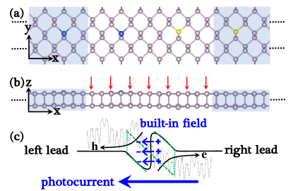
First, we illustrate the geometric structure and schematic of the PVE device: a 2D lateral PN homojunction based on MBP. As shown in Fig.1(a), the PN homojunction is formed by chemically doping Si (blue atoms) and S (yellow atoms) in different regions of MBP, which extends to . Here atom substitution doping is considered. In the -direction, vacuum regions are maintained larger than 15 Å in order to avoid spurious interactions. Periodic boundary conditions are applied in the - and -directions. Next, geometric optimization is conducted using the Vienna Simulation Package (VASP) based on DFT.(Kre1996, ; Kre1996a, ) Generalized gradient approximation (GGA) with the Perdew-Burke-Ernzerhof (PBE)(Per1996, ) parametrization is selected as the exchange-correlation functional. Projector augmented wave (PAW) method is utilized to simulate electron-ion interactions.(Bloechl1994, ; Kre1999, ) The plane wave cutoff energy is set as 500 eV. The structure is fully relaxed until the force on each atom is less than 0.01 eV/Å. Since the atoms of MBP are not in one plane, we also show the side view of the MBP-based device in Fig.1(b).
The device is divided into three regions: the central region and the semi-infinite left/right leads. The central region is vertically irradiated by PL (the red arrows). The Fermi energy of the P region is lower than that of the N region due to the atom doping. However, when the P and N regions are coupled with each other, the Fermi energy of the P/N region increases/decreases through the effective potential energy of the central region and forms the curved Fermi level near the PN junction. The effective potential energy along the -direction is plotted as the background (the light gray line). As shown in Fig.1(c), the curved Fermi level leads to the built-in electric field near the joint of the PN junction. From the potential decline (the green dash line), we can estimate the acting range and the strength of the built-in field. While excited by photons, the - pairs offer effective transport carriers. Driven by the built-in electric field (the blue arrows), electrons/holes flow into the right/left leads and generate a photocurrent.
Subsequently, we calculate the photocurrent using the first-principles quantum transport package, , which is based on NEGF-DFT.(Taylor2001, ; Taylor2001a, ; hzw, ) Norm conserving pseudopotentials are used to describe the atom cores, and double- polarized (DZP) atomic orbitals are taken as basis sets.(Tro1991, ; Soler2002, ) GGA with the form of PBE is selected as the exchange-correlation potential. The NEGF-DFT self-consistent Hamiltonian is obtained when monitored quantities, such as every element in the Hamiltonians and the density matrices, differ by less than eV between two iteration steps. The calculation of photocurrent involves two steps in order: (1) the Hamiltonian of the two-lead device without photons is obtained self-consistently by the NEGF-DFT formalism; (2) the electron-photon (e-p) interaction is perturbatively included as self energy during the photocurrent calculation.
Photocurrent flowing from the right lead to the central region can be written in terms of the NEGF in the following form (Chen2012, ; Zhang2014, ; Xie2015, )
| (1) |
where is the electron charge and is the Plank constant, respectively. is the line width function of the right lead, and is its Fermi-Dirac distribution function. is the greater/lesser Green’s function, which is expressed asHen2002
| (2) |
where is the light velocity, is the reduced Plank constant, and is the vacuum dielectric constant. and are the relative magnetic susceptibility and the relative dielectric constant, respectively. is the light intensity defined as the number of photons per unit time per unit area. is the static electron mass. and are the retarded/advanced and greater/lesser Green’s functions without photons, respectively. originates from the self energies of e-p interactions. The matrix denotes the projection of the electron momentum on the polarization direction and atom site which is perpendicularly irradiated by PL. For concise expression, we omit atom site in the following content. For linearly polarized light (LPL) or elliptically polarized light (EPL), or , where is the cartesian component of the electron momentum. Substituting the expression of , we have
| (3) |
for LPL, and
| (4) |
for EPL, respectively. The quadratic terms “” and “” with the factor are identical for LPL and EPL, whereas the cross terms “” and “” labeled by are different for LPL and EPL. Polarization angle of the incident light is labeled in Fig.2(a).
In order to investigate the photoelectric response properties, we define the normalized photocurrent,(Hen2002, ; Chen2012, ) i.e., the photoresponse function . It is easy to show that has the dimension of area. In our calculation, the unit of length is Bohr radius , and hence is measured in the unit of . Suppose the photon energy eV, and the optical energy flux density , the photoresponse function should be equivalent to the photocurrent .
In our MBP-based homojunction device, SIS is completely broken by the PN junction, which leads to the greatly enhanced photocurrent. But there is approximate mirror symmetry along the -direction, since the acceptor atom Si and donor atom S are approximately located long the straight line in -direction. As a result, is nearly symmetric at . These results suggests that, the cross term of labeled by is negligible, i.e., the and terms are approximately zero; the photocurrent is mainly determined by the square terms “” and “”. Consequently, according to Eqs.(3) and (4), photocurrents induced by LPL or EPL exhibit similar behaviors. depends mostly on the square terms related to , and hence it is nearly symmetric about and . These analysis will be numerically verified in the following section.
III Numerical results and discussion
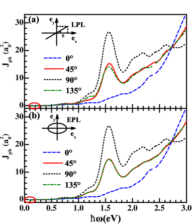
In this section, we present simulation results on the photoelectric properties of the MBP homojunction device. We first investigate the dependence of photocurrent on photon energy and polarization angle . Fig.2 shows the photocurrent versus for different , where LPL and EPL induced photocurrents are shown in panels (a) and (b), respectively. It is obvious that the photocurrents for LPL and EPL show similar behaviors, which agrees with our analysis in Sec.II. Since is nearly symmetric about and , we see from Fig.2 that . Considering the similarity of LPL and EPL induced photocurrents, in the rest of the content, we focus on the photoresponse of EPL. Fig.2(b) shows that, the behavior of is distinct in different photon energy ranges. We have the following observations: (1) is nearly zero when eV, which is reasonable for a semiconductor; (2) shows a peak around eV for ; (3) with the increasing of from to , increases when eV and decreases when eV; (4) When eV, photocurrent flows in the opposite direction, i.e., , as shown by the red ovals in Fig.2.
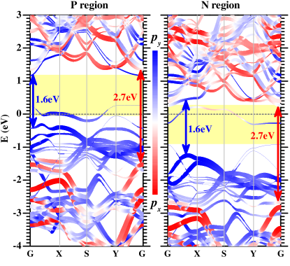
Next, we analyze the above phenomena through the projected band structures for the P and N regions, which are plotted in Fig.3. The thickness of curves denotes the total contribution of orbitals and , and the red and blue colors denote the relative proportion of and . Due to the wrinkle structure of MBP, its in-plane orbitals and widely contribute to the whole band structure, which leads to orbital-resolved photoelectric phenomenon. In the left lead of the homojunction (P region), phosphorus is partially substituted by Si, where negatively charged acceptor ions accumulate and the Fermi level is lowered. In contrast, Fermi level in the right lead (N region) is lifted. When coupled with each other, the Fermi energies of P and N regions are balanced at eV, at which the hybrid bands with contribution from the dopant atoms also reside. Fig.3 shows that the Fermi energy crossing the impurity level of the P/N region is closer to the valence/conduction band, since the band structure of the P/N region is shifted up/down. In Fig.3, the energy gap is marked by the light yellow region, from which we can estimate that the relative shift is about 0.95 eV. This means the potential barrier induced by charge accumulation near the PN junction is approximately 0.95 eV. To generate a nonzero photocurrent, the charge carriers must overcome this barrier. Therefore, significantly increases when eV, as shown in Fig.2.
Photon-excited pairs contribute to the photocurrent carriers, where pairs are composed of holes in the valence band and electrons in the conduction band. From Fig.3, we can find the curves near the top of valence band are blue (), which means the in-plane orbital is dominant for the holes here. Meanwhile, the curves far below the valence band top as well as those near the conduction band bottom are red and blue (+), which indicates that the carriers in these bands possess nearly equal component of and . According to the quantum selection rule, the electrons and holes in pairs must have the same orbital. In Fig.3, we mark the possible direct transitions from the valence to the conduction bands, i.e., (blue block arrows) and (red block arrows). Photon energy eV is a critical value, which determines the transition is dominated by (below 2.7 eV) or (above 2.7 eV). On the premise of the selection rule, the more the orbital element, the larger the photocurrent. For eV (blue arrows), the element is dominant for the holes near the valence band top, and thus reaches the local maximum for , as shown in Fig.2.
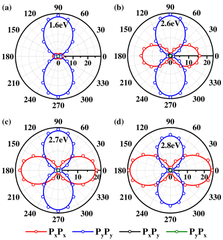
Due to the interaction, the photocurrent is related to the electron momentum ( and ) through the polarization angle of PL. Considering that the electron moment directly reflects the orbital extension of PL, the photocurrent contributed by different orbitals would have different polarizing angular dependence. Based on these facts, we plot the polarizing angular distribution for the cross and square terms of the photocurrent in Fig.4. Several typical photon energies are selected: eV (-based is maximum), eV, eV (proportion boundary of and ), and eV. As expected, the cross terms “” and “” are negligible in all panels due to the mirror symmetry along -direction. The square term “” extends along -direction (), while “” spreads along -direction (). For eV, the “” term is near zero, and reaches maximum at . When eV, the “” term prevails, and is in favor of . For eV, the magnitude of “” and “” terms are almost equal, and hence is independent of . Since the PN junction is infinitely extended in -direction, favors orbital . Consequently, when eV, “” is always greater than “”, as shown in Fig.4(d). Hence is larger at when eV (Fig.2) due to the dominant term extends in -direction. All these facts corresponds exactly to those shown in Fig.2.
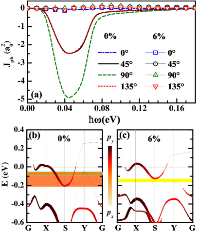
We notice that in the red oval regions of Fig. 2, the photocurrent flows in the opposite directions, i.e., for eV. The photocurrent in this range is magnified in Fig. 5(a). We also plot of strained PN junction with tension , in which is nearly zero at small . Negative is clearly observed when . Driven by the built-in field, should flow from right to left, as displayed in Fig. 1(c). The only possible reason for the reserved photocurrent is that charge carriers are changed from electron to hole, i.e., band inversion occurs. To interpret this abnormal phenomenon, we plot the band structures of the left lead (P region) with tension and in Fig. 5(b) and Fig. 5(c), respectively.
We see that the valence band and the hybrid level of dopant atoms crossed by the Fermi energy overlap with each other (orange region in Fig. 5(b)), leading to the inverse band structure. Through calculation, we find that when increases, the overlap region disappears gradually, and a bandgap emerges. Fig. 5(c) shows the band structure of the left lead with tension . This gapped band structure contrasts with the inverse band structure at . Comparing in the case of and , we can deduce that the inverse band structure induces the reversed photocurrent at small . Furthermore, in the range of small photon energy, the photocurrent is mainly contributed by orbital . If the photon can excite carriers with maximum portion of , PVE will be most efficient and will show a peak. The efficient excitation occurs around eV, which is marked by narrow green gridding in the orange region of Fig. 5(b), where orbital dominates the overlapped band. As a result, reaches the maximum at eV in Fig.5(a).
IV Conclusions
In summary, we have investigated the photoelectric characteristic of a 2D lateral PN homojunction based on monolayer black phosphorus (MBP), which is driven by the photovoltaic effect under the illumination of polarized light (PL). Once the potential barrier near the PN junction is overcome, the excited photocurrent is greatly enhanced by the built-in electric field. The MBP-based PN homojunction device shows high-efficient photovoltaic response in a large photon energy range, from 1 eV to 3 eV. Due to the electron-photon () interaction, electron momentum of the photocurrent is closely related to the in-plane atomic orbitals of MBP. Orbital or dominates the photoelectric response in different photon energy ranges, which leads to the distinct behavior of the photocurrent for different polarization angles of the incident light. These findings indicate that the MBP-based PN homojunction has promising applications in high-efficiency photoelectric devices and orbital-resolved photovoltaic detection.
acknowledgments
This work was supported by the National Natural Science Foundation of China (Grants No.12174023 and No.12174262).
References
- (1) S. D. Ganichev, H. Ketterl, W. Prettl, E. L. Ivchenko, and L. E. Vorobjev, Circular photogalvanic effect induced by monopolar spin orientation in -GaAs/AlGaAs multiple-quantum wells, Appl. Phys. Lett. 77, 3146 (2000).
- (2) S. D. Ganichev, E. L. Ivchenko, S. N. Danilov, J. Eroms, W. Wegscheider, D. Weiss, and W. Prettl, Conversion of Spin into Directed Electric Current in Quantum Wells, Phys. Rev. Lett. 86, 4358 (2001).
- (3) S. D. Ganichev, U. Rössler, W. Prettl, E. L. Ivchenko, V. V. Bel’kov, R. Neumann, K. Brunner, and G. Abstreiter, Removal of spin degeneracy in -SiGe quantum wells demonstrated by spin photocurrents, Phys. Rev. B 66, 075328 (2002).
- (4) H. Ma, C. Jiang, Y. Liu, L. Zhu, X. Qin, and Y. Chen, Tailoring high-frequency magnonics in monolayer chromium trihalides, Appl. Phys. Lett. 102, 232402 (2013).
- (5) D. A. Stewart and F. Léonard, Photocurrents in Nanotube Junctions, Phys. Rev. Lett. 93, 107401 (2004).
- (6) M. Riordan and L. Hoddeson, Origins of the pn junction, IEEE Spectrum 34, 46 (1997).
- (7) J. Chen, Y. Hu, and G. Hong, First-principles analysis of photocurrent in graphene PN junctions, Phys. Rev. B 85, 155441 (2012).
- (8) M. S. Choi, D. Qu, D. Lee, X. Liu, K. Watanabe, T. Taniguchi, and W. J. Yoo, Lateral MoS2 p-n Junction Formed by Chemical Doping for Use in High-Performance Optoelectronics, ACS Nano 8, 9332 (2014).
- (9) Y. Jin, D. H. Keum, S.-J. An, J. Kim, H. S. Lee, and Y. H. Lee, A Van Der Waals Homojunction: Ideal p-n Diode Behavior in MoSe2, Adv. Mater. 27, 5534 (2015).
- (10) Z. Wang, F. Wang, L. Yin, Y. Huang, K. Xu, F. Wang, X. Zhan, and J. He, Electrostatically tunable lateral MoTe2 p-n junction for use in high-performance optoelectronics, Nanoscale 8, 13245 (2016).
- (11) M. Sun, D. Xie, Y. Sun, W. Li, and T. Ren, Locally hydrazine doped WSe2 p-n junction toward high-performance photodetectors, Nanotechnology 29, 015203 (2018).
- (12) G. Wu, X. Wang, Y. Chen, S. Wu, B. Wu, Y. Jiang, H. Shen, T. Lin, Q. Liu, X. Wang, P. Zhou, S. Zhang, W. Hu, X. Meng, J. Chu, and J. Wang, MoTe2 p-n Homojunctions Defined by Ferroelectric Polarization, Adv. Mater 32, 1907937 (2020).
- (13) X. Tao, P. Jiang, H. Hao, X. Zheng, L. Zhang, and Z. Zeng, Pure spin current generation via photogalvanic effect with spatial inversion symmetry, Phys. Rev. B 102, 081402(R) (2020).
- (14) S. Ghosh, A. Varghese, K. Thakar, S. Dhara, and S. Lodha,Enhanced responsivity and detectivity of fast WSe2 phototransistor using electrostatically tunable in-plane lateral p-n homojunction, Nat. Commun. 12, 3336 (2021).
- (15) Y. Li, J. Fu, X. Mao, C. Chen, H. Liu, M. Gong, and H. Zeng, Enhanced bulk photovoltaic effect in two-dimensional ferroelectric CuInP2S6, Nat. Commun. 12, 5896 (2021).
- (16) F. Xu, H. Su, Z. Gong, Y. Wei, H. Jin, and H. Guo, Controllable ferroelectricity and bulk photovoltaic effect in elemental group-V monolayers through strain engineering, Phys. Rev. B 106, 195418 (2022).
- (17) Y. Li, H. Hao, X. Shang, Y.-H. Zhou, and X. Zheng, Realizing Pure Spin Current With Photogalvanic Effect in Zigzag Graphene Nanoribbon Junctions: The Roles of Tetragon and Hexagon Connectors, IEEE Trans. Electron Devices 70, 3908 (2023).
- (18) S. M. Sze and K. N. Kwok, Physics of Semiconductor Devices (Wiley, Hoboken, NJ, USA, 2007).
- (19) E. Samuel Reich, Phosphorene excites materials scientists, Nature 506, 19 (2014).
- (20) L. Li, Y. Yu, G. J. Ye, Q. Ge, X. Ou, H. Wu, D. Feng, X. H. Chen, and Y. Zhang, Black phosphorus field-effect transistors, Nat. Nanotechnol. 9, 372 (2014).
- (21) J. Qiao, X. Kong, Z.-X. Hu, F. Yang, and W. Ji, High-mobility transport anisotropy and linear dichroism in few-layer black phosphorus, Nat. Commun. 5, 4475 (2014).
- (22) K. Gong, L. Zhang, W. Ji, H. Guo, Electrical contacts to monolayer black phosphorus: A first-principles investigation, Phys. Rev. B 90, 125441 (2014).
- (23) F. Xia, H. Wang, and Y. Jia, Rediscovering black phosphorus as an anisotropic layered material for optoelectronics and electronics, Nat. Commun. 5, 4458 (2014).
- (24) X. Wang, A. M. Jones, K. L. Seyler, V. Tran, Y. Jia, H. Zhao, H. Wang, L. Yang, X. Xu, and F. Xia, Highly anisotropic and robust excitons in monolayer black phosphorus, Nat. Nanotechnol. 10, 517 (2015).
- (25) V. Tran, R. Soklaski, Y. Liang, and L. Yang, Layer-controlled band gap and anisotropic excitons in few-layer black phosphorus, Phys. Rev. B 89, 235319 (2014).
- (26) X. Peng, A. Copple, and Q. Wei, Edge effects on the electronic properties of phosphorene nanoribbons, J. Appl. Phys. 116, 144301 (2014).
- (27) A. N. Rudenko and M. I. Katsnelson, Quasiparticle band structure and tight-binding model for single-and bilayer black phosphorus, Phys. Rev. B 89, 201408(R) (2014).
- (28) J. Guan, Z. Zhu, and D. Tománek, Phase Coexistence and Metal-Insulator Transition in Few-Layer Phosphorene: A Computational Study, Phys. Rev. Lett. 113, 046804 (2014).
- (29) V. Wang, Y. Kawazoe, and W. T. Geng, Native point defects in few-layer phosphorene, Phys. Rev. B 91, 045433 (2015).
- (30) Y. Xie, J. Zhao, Y. Hu, X. Ye, Y. Xie, and R. Cao, Outstanding spin-transport properties of a flexible phosphorene photodetector driven by the photogalvanic effect under mechanical strains, Phys. Chem. Chem. Phys. 23, 11961 (2021).
- (31) H. Yuan, X. Liu, F. Afshinmanesh, W. Li, G. Xu, J. Sun, B. Lian, A. G. Curto, G. Ye, Y. Hikita, Z. Shen, S.-C. Zhang, X. Chen, M. Brongersma, H. Y. Hwang, and Y. Cui, Polarization-sensitive broadband photodetector using a black phosphorus vertical p-n junction, Nat. Nanotechnol. 10, 707 (2015).
- (32) X. Guo, L. Zhang, J. Chen, X. Zheng, and L. Zhang, Gate tunable self-powered few-layer black phosphorus broadband photodetector, Phys. Chem. Chem. Phys. 23, 399 (2021).
- (33) S. Li, T. Wang, X. Chen, W. Lu, Y. Xie, and Y. Hu, Self-powered photogalvanic phosphorene photodetectors with high polarization sensitivity and suppressed dark current, Nanoscale 10, 7694 (2018).
- (34) S. Jeon, J. Jia, J. H. Ju, and S. Lee, Black phosphorus photodetector integrated with Au nanoparticles, Appl. Phys. Lett. 115, 183102 (2019).
- (35) Y. Luo, Y. Xie, X. Ye, and Y. Wang, A self-powered phosphorene photodetector with excellent spin-filtering and spin-valve effects, Phys. Chem. Chem. Phys. 21, 7613 (2019).
- (36) J. Zhao, Y. Hu, Y. Xie, L. Zhang, and Y. Wang, Largely Enhanced Photogalvanic Effects in a Phosphorene Photodetector by Strain-Increased Device Asymmetry, Phys. Rev. Applied 14, 064003 (2020).
- (37) N. Youngblood and M. Li, Ultrafast photocurrent measurements of a black phosphorus photodetector, Appl. Phys. Lett. 110, 051102 (2017).
- (38) Y. Xie, M. Chen, Z. Wu, Y. Hu, Y. Wang, J. Wang, and H. Guo, Two-Dimensional Photogalvanic Spin-Battery, Phys. Rev. Applied 10, 034005 (2018).
- (39) Q. Wu, L. Shen, M. Yang, Y. Cai, Z. Huang, and Y. P. Feng, Electronic and transport properties of phosphorene nanoribbons, Phys. Rev. B 92, 035436 (2015).
- (40) M. Buscema, D. J. Groenendijk, S. I. Blanter, G. A. Steele, H. S. J. van der Zant, and A. Castellanos-Gomez, Fast and Broadband Photoresponse of Few-Layer Black Phosphorus Field-Effect Transistors, Nano Lett. 14, 3347 (2014).
- (41) M. Buscema, D. J. Groenendijk, G. A. Steele, H. S. J. van der Zant, and A. Castellanos-Gomez, Photovoltaic effect in few-layer black phosphorus PN junctions defined by local electrostatic gating, Nat. Commun. 5, 4651 (2014).
- (42) Y. Xu, J. Yuan, L. Fei, X. Wang, Q. Bao, Y. Wang, K. Zhang, and Y. Zhang, Selenium-Doped Black Phosphorus for High-Responsivity 2D Photodetectors, Small 12, 5000 (2016).
- (43) W. Lv, B. Yang, B. Wang, W. Wan, Y. Ge, R. Yang, C. Hao, J. Xiang, B. Zhang, Z. Zeng, and Z. Liu, Sulfur-Doped Black Phosphorus Field-Effect Transistors with Enhanced Stability, ACS Appl. Mater. Interfaces 10, 9663 (2018).
- (44) Y. Yu, B. Xing, J. Yao, X. Niu, Y. Liu, X. Wu, X. Yan, M. Li, J. Sha, and Y. Wang, N-type doping of black phosphorus single crystal by tellurium, Nanotechnology 31, 315605 (2020).
- (45) S. Jalaei, J. Karamdel, and H. Ghalami-Bavil-Olyaee, Mid-Infrared Photodetector Based on Selenium-Doped Black Phosphorus, Phys. Status Solidi A 217, 2000483 (2020).
- (46) H. Hu, Z. Shi, K. Khan, R. Cao, W. Liang, A. K. Tareen, Y. Zhang, W. Huang, Z. Guo, X. Luo, and H. Zhang, Recent advances in doping engineering of black phosphorus, J. Mater. Chem. A 8, 5421 (2020).
- (47) G. Kresse and J. Furthmüller, Efficient iterative schemes for ab initio total-energy calculations using a plane-wave basis set Phys. Rev. B 54, 11169 (1996).
- (48) G. Kresse and J. Furthmüller, Efficiency of ab-initio total energy calculations for metals and semiconductors using a plane-wave basis set, Comput. Mater. Sci 6, 15 (1996)
- (49) J. P. Perdew, K. Burke, and M. Ernzerhof, Generalized Gradient Approximation Made Simple, Phys. Rev. Lett. 77 ,3865 (1996).
- (50) P. E. Blochl, Projector augmented-wave method, Phys. Rev. B 50, 17953 (1994).
- (51) G. Kresse and D. Joubert, From ultrasoft pseudopotentials to the projector augmented-wave method, Phys. Rev. B 59, 1758 (1999).
- (52) J. Taylor, H. Guo, and J. Wang, Ab initio modeling of quantum transport properties of molecular electronic devices, Phys. Rev. B 63, 245407 (2001).
- (53) J. Taylor, H. Guo, and J. Wang, Ab initio modeling of open systems: Charge transfer, electron conduction, and molecular switching of a device, Phys. Rev. B 63, 121104(R) (2001).
- (54) http://hzwtech.com.
- (55) N. Troullier and J. L. Martins, Efficient pseudopotentials for plane-wave calculations, Phys. Rev. B 43, 1993 (1991).
- (56) J. M. Soler, E. Artacho, J. D. Gale, A. García, J. Junquera, P. Ordejón, and D. Sánchez-Portal, The SIESTA method for ab initio order-N materials simulation, J. Phys: Condens. Matter 14,2745 (2002).
- (57) L. Zhang, K. Gong, J. Chen, L. Liu, Y. Zhu, D. Xiao, and H. Guo, Generation and transport of valley-polarized current in transition-metal dichalcogenides, Phys. Rev. B 90, 195428 (2014).
- (58) Y. Xie, L. Zhang, Y. Zhu, L. Liu, and H. Guo, Photogalvanic effect in monolayer black phosphorus, Nanotechnology 26, 455202 (2015).
- (59) L. E. Henrickson, Nonequilibrium photocurrent modeling in resonant tunneling photodetectors, J. Appl. Phys 91, 6273 (2002).