Laser Writing of Parabolic Micromirrors with a High Numerical Aperture
for Optical Trapping and Rotation
Abstract
On-chip optical trapping systems allow for high scalability and lower the barrier to access. Systems capable of trapping multiple particles typically come with high cost and complexity. Here we present a technique for making parabolic mirrors with micron-size dimensions and high numerical apertures (NA>1). Over 350 mirrors are made by simple CO2 laser ablation of glass followed by gold deposition. We fabricate mirrors of arbitrary diameter and depth at a high throughput rate by carefully controlling the ablation parameters. We use the micromirrors for 3-dimensional optical trapping of microbeads in solution, achieving a maximum optical trap stiffness of 52 pN/µm/W. We then further demonstrate the viability of the mirrors as in-situ optical elements through the rotation of a vaterite particle using reflected circularly polarized light. The method used allows for rapid and highly customizable fabrication of dense optical arrays.
There has been a great interestZhu et al. (2019); Ozcelik et al. (2017) in developing optical lab-on-a-chip platforms in recent years as they are portable, robust, and scalable. Integrating multiple optical components has allowed great leaps in analyzing and sensing biological specimensPadgett and Di Leonardo (2011); Huang et al. (2015); Chen and Shamsi (2017). One such powerful technique is optical trapping, which allows for the 3D manipulation of objects by using the transfer of momentum of lightAshkin (1970). As a well-established technique, it has found uses in single-molecule force spectroscopyCampugan et al. (2020); Wang et al. (1997), particle sortingMacDonald et al. (2003); Leake et al. (2013), and sensing in both the far and near fieldBouloumis and Chormaic (2020). An optical trap is characterized by the trap stiffness , assuming the trapped particle is in a harmonic motionNeuman and Block (2005). Furthermore, it is possible to transfer the angular momentum of light to anisotropic particles through external or internal birefringence, inducing rotation when trapped by a circularly polarized beam.Arita et al. (2013); Bruce et al. (2021)
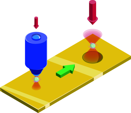
The system must meet several requirements to allow for the confinement of the subject specimen in an optical potential in the far field: the particle must be of a higher refractive index than the surrounding medium and, for optimal performance, should be of a size comparable to that of the wavelength of the trapping beamMetzger et al. (2011); Rohrbach (2005). In addition, a tightly focused beam is necessary to provide a large enough restoring force for trapping. A bulky, high numerical aperture (NA) and high magnification microscope objective is required, with multiple drawbacks. For one, the objective size makes the integration difficult, and the high magnification brings a small field of view, limiting the number of simultaneously manipulated samples. These and the high cost of high-NA objectives have resulted in the poor integration and scalability of the optical trapping platform.
Multiple schemes have been developed in the last two decades to address these issues to enable on-chip trappingPaiè et al. (2018). These include creating an optical lattice through interferenceMacDonald et al. (2003), near and far field trapping enabled by fibersLou et al. (2019), as well as working to replace the microscope objective with a high numerical aperture but a much smaller optical lens equivalent, capable of similar focusing performance. The best performing have been metasurfacesXiao et al. (2023), placed at the bottom of the microfluidic chamber for trapping in reflectionXiao et al. (2023); Tkachenko et al. (2018), grafted on top for trapping in transmissionShen et al. (2021) or placed on tips of optical fibersPlidschun et al. (2021). With NA ranging from 0.56 to 1.2Markovich et al. (2018); Xiao et al. (2023) , they can reach a performance almost matching that of high NA objectives, all while keeping a small footprint of mm2. Another option is the Fresnel diffractive elementsSun et al. (2007); Kuo and Hu (2011); Schonbrun et al. (2008). However, for both systems, the fabrication process is time-consuming and expensive. Additionally, the small and delicate optical elements which make up these lenses can be easily damaged. Depending on the geometry, they will be wavelength-specific and polarization sensitive. Microlenses and micromirrorsSow et al. (2004); Merenda et al. (2007), however, do not suffer from these problems. By imprinting pre-made lensesZhao et al. (2011); Merenda et al. (2009), arrays of traps with relatively high NA have been fabricated. While convenient, this method is limited by the variety of lenses available to consumers. Chemical treatment can also be combined with other techniques to etch smooth mirrors into the substrateMatsutani et al. (2019); Kendall et al. (1988); Moktadir et al. (2004); Najer et al. (2017). A method often combined with etching is silica CO2 laser ablation, a well-established glass treatment process whereby a short (100 ns) pulse is used to form an approximately hemispherical mirrorRuelle et al. (2019). Silica is exceptionally absorbent for radiation above 4 µmFeit and Rubenchik (2003), meaning that a focused beam of CO2 laser with a wavelength of 10.6 µm can evaporate the glass directly at the focus, melting the glass around it. The vapor pressure from the evaporation then creates a melt front which travels away from the center until the glass re-solidifies, the entire process occurring in under a secondHunger et al. (2012); Nowak et al. (2006).
Here, we present a significantly faster, more customizable technique for creating trapping arrays with high numerical aperture. Using a continuous wave (CW) CO2 laser, we write micromirror structures through ablation. First, we expose the glass substrate for 100 ms to a focused TEM00 mode of the laser, resulting in a nearly parabolic mirror profileHunger et al. (2010). The glass is then coated with a thin gold layer to achieve a smooth reflective surface. We show that by tuning the ablation parameters, the diameter and depth of the micromirrors can be controlled accurately based on the required application. To demonstrate the platform’s viability, we use a high NA micromirror to trap 5 µm vaterite and 2 µm silica particles suspended in D2O. As shown in Fig. 1, we use a hybrid optical setup that interchangeably allows trapping by a high NA objective or micromirrors. While not necessary to enable trapping, it is convenient for this demonstration, as trapping can be performed passively by illuminating using a collimated beam. We characterize the optical performance of the mirror, then proceed to use it to reverse the direction of rotation of a vaterite particle. Through this, we demonstrate the potential of micromirrors as a simple-to-fabricate and versatile lab-on-chip optical platform.
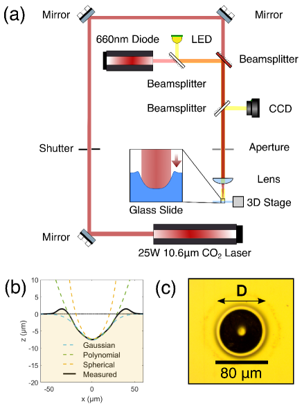
At the core of the setup for the fabrication of the micromirrors is the CO2 ablation laser (Synrad 48-KA CW 25 W) (see Fig. 2(a)). We controlled the duration of the ablation using a mechanical shutter (Thorlabs SC10) and set the average power through the duty cycle of the laser (8%, corresponding to 1.2 W at the sample plane). The glass sample was mounted vertically on a motorized 3D stage (Newport, Picomotor actuators). A visible diode laser ( = 660 nm) with an adjustable divergence was used as a guide to precisely locate the x, y, and z positions of the focused CO2 laser beam on the sample. For monitoring, we used a CMOS camera (Thorlabs DCC1545M) in conjunction with a collimated light-emitting diode. The shutter, CO2 laser, and stage were synchronized and controlled using LabVIEW to rapidly fabricate customized arrays of micromirrors, as shown in S1. The automation also allowed for writing continuous channels in glass, as shown in S2. The beam profile of the CO2 laser was spatially filtered using an aperture and finally focused onto the glass sample to a size of 100 µm using a ZnSe plano-convex lens ( = 15 mm), which also served as the imaging lens for the camera. After ablation, the sample was transferred to an electron beam evaporator (Edwards AUTO 306), where a 2 nm thick adhesion layer of NiCr was deposited, followed by 150 nm of gold. We characterized the micromirrors using optical microscopy and a surface profiler. We used optical microscopy to extract the mirror diameter and depth (Fig. 2(b)) and a contact mode profilometer (Veeco Dektak 150 with a 12 µm stylus) to accurately map the profile (Fig. 2(c)). The figure shows the micromirror used for particle trapping with depth = 7.3 µm and diameter = 56.5 µm. The mirror profile resembles the Gaussian intensity profile of the CO2 beam with deviations due to the long pulse durations used, meaning that a parabola more accurately describes the profileHunger et al. (2012). The exact scan geometry and alternative view of the profile are shown in S3. 357 micromirrors with diameters of 40-120 µm were fabricated and characterized. We considered five parameters: the laser power, the position of the focus relative to the substrate, the duration and the number of exposures, and the size of the aperture (shown in Fig. 2(a)). We found that the final profile of the micromirror was relatively insensitive to the duration and number of exposures, indicating that the shortest exposure created by the shutter (50 ms) was longer than the ablation timescale. In addition, the diameter of the micromirrors initially displayed a simple linear relationship with the laser power, which plateaued as the mirrors’ diameter approached that of the focused beam. Finally, the depth of the micromirrors reached an upper bound at higher laser power (2 W), where the rapid change in temperature gradient resulted in cracks forming at the bottom of the mirrors. Furthermore, the diameter and the depth of the micromirrors had a nearly linear dependence on the aperture diameter. The exact position of the focus had the most substantial effect on the micromirror profile. If the mirror’s center evaporated too quickly, it formed a secondary curvature inside the first, as the melt front would not move fast enough. Hence, the beginning of each fabrication included a calibration step where the exact z-plane was chosen based on the mirror shape observed through the CCD after ablation. For further information on mirror ablation, see supplementary figures S4 – S7.
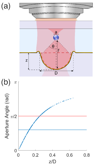
To translate the measurable mirror diameter and depth into a usable metric of NA, we used a geometric approximation following profile measurements which clearly showed a parabolic profile of the mirror, as seen in Fig. 2(c). The focal length f of the parabola isLindlein et al. (2007):
| (1) |
where is the mirror diameter, and is the depth. We define the aperture angle of a parabolic mirror as:
| (2) |
We clearly show the relationship between and in Fig. 3(b), where the parameters of 357 mirrors are plotted according to their estimated aperture angle. Of course, this is a simple geometric approximation. Especially for higher ratios of and , the effects of higher fabrication power causing cracks and uneven surfaces must be considered. It is also important to note that as increases over degrees, the trapping decreases in quality as more of the light contributes to the scattering force incident on the particle. For mirrors with , a comparison can be made to a lens, using NA as the figure of merit. Taking the relationship between NA and to be where is the refractive index of the medium (1.33 for D2O), we can define an effective NA of the micromirrors defined as:
| (3) |
It is important to note that this comparison with lenses is only valid for mirrors where , whereas for an infinitely extending parabolic mirror, approaches .
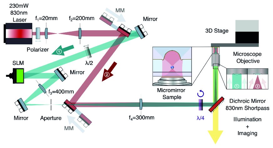
The hybrid setup used for trapping and rotating the particles is shown in Fig. 4. The trapping laser (Omicron LuXx) had a total power of 230 mW at 830 nm and was linearly polarized (Thorlabs LPNIRB050), after which the beam was expanded by ten times using a telescope. The laser beam could then follow one of two paths depending on whether trapping by the objective (Path 1) or micromirrors (Path 2) was required. Path 1 (marked in blue in Fig. 4) uses a half-wave plate to match the beam’s polarization to that of a spatial light modulator (SLM, Meadowlark 1920x1152) for moving the tweezers. The beam was then sent through a 4 system conjugating the plane of the SLM and the back focal plane of an inverted water immersion objective (Olympus UPLANSAPO, 60x, NA = 1.2). The use of the SLM was not necessary but allowed for the convenient alignment of the particle and mirror illumination when switching paths. For the rotation of particles, the beam was circularly polarized using a quarter-wave plate to allow for the transfer of angular momentum to birefringent particles. Path 2 (marked in red) could be switched using a pair of mirrors placed on a motorized linear stage (Thorlabs ELL20). The beam was then focused onto the back of the microscope objective (Fourier plane) using a lens ( = 300 mm) and the quarter-wave plate for circular polarization. In this way, the incident beam onto the micromirrors would be collimated and circularly polarized. The illumination consisted of a fiber-coupled LED, and the imaging used a CCD camera (Basler acA640-750um) with an 800 nm short-pass filter in front of it.
The microfluidic chamber containing the mirrors and particles was prepared by placing a 100 µm thick vinyl spacer with a hole in the middle to create a well around the mirrors, then depositing the solution of particles, placing a cover slip on top and sealing the edges using nail varnish. The schematic is shown in S8. Particle loading on micromirrors consisted of first trapping a particle (either silica or vaterite) using the high-NA microscope objective (path 1), then delivering it 5 µm below the focal point of the micromirrors. Next, path 2 was switched, resulting in a collimated beam illuminating the entire micromirror, forming the optical trap (see Supplemental Video SV1). The handover from objective to micromirror would take <1 s.
To quantify the quality of the trapping in the micromirror (see Table 1 for parameters), the mirror’s trap stiffness was calculated. For all trapping stiffness comparisons, µm particles (Duke Standards) were used to ensure consistency. First, five videos were taken of the trapped particle at 15 different powers, each video being 10 s long and having a framerate of 1000 fps resulting in 50,000 frames containing information about the position variation of the particle for a given power. Next, the exact x and y positions of the center of mass of the particles were extracted using a previously demonstrated scheme using the shift property of the Fourier transform to symmetrize all images and obtain their relative displacementLeite et al. (2018). A power spectrum density of the positions was then plotted and fitted with a Lorentzian to acquire a corner frequency , which was then converted to a trap stiffness throughNeuman and Block (2005):
| (4) |
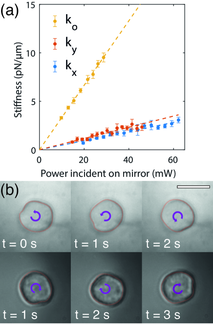
where is the viscosity of D2O (1.247 mPas at room temperature), and is the particle’s radius. Heavy water was used due to a lower absorption coefficient at higher wavelengthsBraun and Smirnov (1993). No proximity correction was necessary as the particle was situated directly in the middle of the chamber. Five stiffness values were obtained for each power, then averaged and plotted against the power measured after the microscope objective (see Fig. 5(a)). The dashed line is a straight-line fit with no intercept, which yielded a stiffness = (521) pN/µm/W, when correcting for the size of the beam incident on the mirror (see S9). The value is nearly six times lower than that of the objective with NA = 1.2 with a stiffness of = (3322 pN/µm/W). An image and diagram of the beam profile can be found in S10, showing a FWHM of 630 nm. Thermal effects are an obvious concern due to the presence of gold: multiple studies have shown that a significant effect from heating is experienced by particles less than a few microns away from the surface, with a focused beam incident on the gold surfaceLu et al. (2021); Xu et al. (2018); Wang et al. (2022). However, in our case, the particle is over 50 µm above the gold surface, the beam is dispersed across an area orders of magnitude larger, and combined with the linear response to changes to the laser power, thermal currents are not expected to have contributed to the trapping dynamics. Also, although the coherence length of our laser would allow for interference, given the relative intensity of the incident collimated beam and the reflective focused beam at the location of the trapping, we exclude the effects of standing waves. Given the wavelength of 830 nm resulting in fringes every 415 nm, and the depth of field of our objective of 800 nm, we would also have seen the significant displacement of the particle in z, which is absent.
| D (µm) | z (µm) | (µm) | ROC (µm) | NA | (pN/µm/W) |
| 56.5 | 7.3 | 54.7 | 109.4 | 1.08 | 521 |
To further show the potential of our platform as a versatile alternative to a microscope objective, we demonstrated its ability to reverse the preferred direction of rotation of a 5 µm piece of vaterite. While microvaterite has been shown to reach rotation speeds of up to 5 MHz in vacuumArita et al. (2013) and up to 400 Hz in waterBishop et al. (2004), the rate is highly dependent on the power at the sample plane and the particle size (typically in 100s of nm). In our demonstration, we place a quarter-wave plate before the objective at 45 degrees with respect to the direction of linear polarization to ensure circular polarization and verify the circularity using a polarimeter (Thorlabs PAX1000IR1) before and after the objective. We first trap the vaterite using objective-enabled optical tweezers and observe the clockwise rotation of the particle, as shown in the bottom panel of Fig. 5(b) and SV2. We then switch the optical path to trap using the micromirror and observe the particle change in the direction of rotation, as shown in the top panel of Fig.5(b) and SV3. To simplify the trapping process, we used relatively large pieces of vaterite (5 µm diameter), which were quite asymmetric. These conditions, combined with the low power of our system (<30 mW vs. typical W usedArita et al. (2016)), means that we observed the particle exhibit a preferred axis of rotation. This is clearly seen in SV2 and SV3 and manifests through a non-uniform rotation rate. We have also considered the role of the angle of reflection on the circular polarization of the reflected beam, as while the effect of reflection from a plane is understood, the case is not as clear for a curved surface such as a parabolic mirrorMansuripur et al. (2011). While this would be a concern for extreme angles, as can be seen in S3(b) most of the reflections from the mirror happen for , where significant differences between s and p components of the polarization could become apparent.
In conclusion, we describe the rapid and versatile fabrication process of 357 high-NA parabolic micromirrors with diameters in the range of 80 µm using CW CO2 laser ablation of silica, followed by gold coating. We show that the micromirrors can be used as a substitute for microscope objectives for optical trapping. We thoroughly analyze the trapping performance at multiple powers, yielding an average stiffness of = (521) pN/µm/W for a mirror with an effective NA = 1.08 comparable with values in the literatureRohrbach (2005); Yang et al. (2021). Finally, we demonstrate the ability of the mirror to counter-rotate a vaterite particle. The mirror geometry is promising in creating integrated dual-beam trappingThalhammer et al. (2011). As closely spaced arrays of arbitrary size can be fabricated, this scheme is a promising technique for on-chip particle trapping and sorting and optical lattices for atoms Bandi et al. (2008); Mu et al. (2009); Sondermann et al. (2020). Similar schemes have also shown great promise regarding the parametric cooling of particles in vacuumVovrosh et al. (2017). With an added laser writing capability, we envisage that guiding particles in arbitrary circuits by 2D trapping in channels would now be feasible in this platform.
See Supplementary Information for videos of particle trapping and rotation, fabrication and characterization details.
This work was supported by the UK Engineering and Physical Sciences Research Council (EP/P030017/1 and EP/S014403/1), by the European Research Council (ERC) under the European Union Horizon 2020 Research and Innovation Program (Grant Agreement No. 819346). HO acknowledges support from the Carnegie Trust for Universities of Scotland (Grant No. RIG007685). KD acknowledges support from the Australian Research Council (Grant No. DP220102303).
The data that support the findings of this study are openly available in the Data Set of the University of St. Andrews Research Portal at https://doi.org/10.5194/essd-10-1807-2018.
References
References
- Zhu et al. (2019) J. M. Zhu, X. Q. Zhu, Y. F. Zuo, X. J. Hu, Y. Shi, L. Liang, and Y. Yang, Opto-Electronic Advances 2, 1 (2019).
- Ozcelik et al. (2017) D. Ozcelik, H. Cai, K. D. Leake, A. R. Hawkins, and H. Schmidt, Nanophotonics 6, 647 (2017).
- Padgett and Di Leonardo (2011) M. Padgett and R. Di Leonardo, Lab on a Chip 11, 1196 (2011).
- Huang et al. (2015) J. A. Huang, Y. L. Zhang, H. Ding, and H. B. Sun, Advanced Optical Materials 3, 618 (2015).
- Chen and Shamsi (2017) S. Chen and M. H. Shamsi, Journal of Micromechanics and Microengineering 27 (2017).
- Ashkin (1970) A. Ashkin, Physical Review Letters 24, 156 (1970).
- Campugan et al. (2020) C. A. Campugan, K. R. Dunning, and K. Dholakia, Contemporary Physics 61, 277 (2020).
- Wang et al. (1997) M. D. Wang, H. Yin, R. Landick, J. Gelles, and S. M. Block, Biophysical Journal 72, 1335 (1997).
- MacDonald et al. (2003) M. P. MacDonald, G. C. Spalding, and K. Dholakia, Nature 426, 421 (2003).
- Leake et al. (2013) K. D. Leake, B. S. Phillips, T. D. Yuzvinsky, A. R. Hawkins, and H. Schmidt, Optics Express 21, 32605 (2013).
- Bouloumis and Chormaic (2020) T. D. Bouloumis and S. N. Chormaic, Applied Sciences (Switzerland) 10 (2020).
- Neuman and Block (2005) K. C. Neuman and S. M. Block, Rev Sci Instrum. 75 (2005).
- Arita et al. (2013) Y. Arita, M. Mazilu, and K. Dholakia, Nature Communications 4, 1 (2013).
- Bruce et al. (2021) G. D. Bruce, P. Rodríguez-Sevilla, and K. Dholakia, Advances in Physics: X 6 (2021).
- Metzger et al. (2011) N. K. Metzger, M. Mazilu, L. Kelemen, P. Ormos, and K. Dholakia, Journal of Optics 13, 044018 (2011).
- Rohrbach (2005) A. Rohrbach, Physical Review Letters 95, 168102 (2005).
- Paiè et al. (2018) P. Paiè, T. Zandrini, R. M. Vázquez, R. Osellame, and F. Bragheri, Micromachines 9, 1 (2018).
- Lou et al. (2019) Y. Lou, D. Wu, and Y. Pang, Advanced Fiber Materials 1, 83 (2019).
- Xiao et al. (2023) J. Xiao, T. Plaskocinski, M. Biabanifard, S. Persheyev, and A. Di Falco, ACS Photonics (2023).
- Tkachenko et al. (2018) G. Tkachenko, D. Stellinga, A. Ruskuc, M. Chen, K. Dholakia, and T. F. Krauss, Optics Letters 43, 3224 (2018).
- Shen et al. (2021) K. Shen, Y. Duan, P. Ju, Z. Xu, X. Chen, L. Zhang, J. Ahn, X. Ni, and T. Li, Optica 8, 1359 (2021).
- Plidschun et al. (2021) M. Plidschun, H. Ren, J. Kim, R. Förster, S. A. Maier, and M. A. Schmidt, Light: Science and Applications 10 (2021).
- Markovich et al. (2018) H. Markovich, I. I. Shishkin, N. Hendler, and P. Ginzburg, Nano Letters 18, 5024 (2018).
- Sun et al. (2007) Y. Y. Sun, X. C. Yuan, L. S. Ong, J. Bu, S. W. Zhu, and R. Liu, Applied Physics Letters 90, 13 (2007).
- Kuo and Hu (2011) J. N. Kuo and H. Z. Hu, Japanese Journal of Applied Physics 50 (2011).
- Schonbrun et al. (2008) E. Schonbrun, C. Rinzler, and K. B. Crozier, Applied Physics Letters 92, 1 (2008).
- Sow et al. (2004) C. H. Sow, A. A. Bettiol, Y. Y. Lee, F. C. Cheong, C. T. Lim, and F. Watt, Applied Physics B: Lasers and Optics 78, 705 (2004).
- Merenda et al. (2007) F. Merenda, J. Rohner, and J.-m. Fournier, Optics Express 15, 101 (2007).
- Zhao et al. (2011) X. Zhao, Y. Sun, J. Bu, S. Zhu, and X. C. Yuan, Applied Optics 50, 318 (2011).
- Merenda et al. (2009) F. Merenda, M. Grossenbacher, S. Jeney, L. Forró, and R.-p. Salathé, Optics letters 34, 1063 (2009).
- Matsutani et al. (2019) A. Matsutani, M. Sato, K. Hasebe, and A. Takada, Sensors and Materials 31, 1325 (2019).
- Kendall et al. (1988) D. L. Kendall, G. R. de Guel, S. Guel-Sandoval, E. J. Garcia, and T. A. Allen, Applied Physics Letters 52, 836 (1988).
- Moktadir et al. (2004) Z. Moktadir, E. Koukharenka, M. Kraft, D. M. Bagnall, H. Powell, M. Jones, and E. A. Hinds, Journal of Micromechanics and Microengineering 14, S82 (2004).
- Najer et al. (2017) D. Najer, M. Renggli, D. Riedel, S. Starosielec, and R. J. Warburton, Applied Physics Letters 110, 011101 (2017).
- Ruelle et al. (2019) T. Ruelle, M. Poggio, and F. Braakman, Applied Optics 58, 3784 (2019).
- Feit and Rubenchik (2003) M. D. Feit and A. M. Rubenchik (2003).
- Hunger et al. (2012) D. Hunger, C. Deutsch, R. J. Barbour, R. J. Warburton, and J. Reichel, AIP Advances 2 (2012).
- Nowak et al. (2006) K. M. Nowak, H. J. Baker, and D. R. Hall, Appl. Opt. 45, 162 (2006).
- Hunger et al. (2010) D. Hunger, T. Steinmetz, Y. Colombe, C. Deutsch, T. W. Hänsch, and J. Reichel, New Journal of Physics 12 (2010).
- Lindlein et al. (2007) N. Lindlein, R. Maiwald, H. Konermann, M. Sondermann, U. Peschel, and G. Leuchs, Laser Physics 17, 927 (2007).
- Leite et al. (2018) I. T. Leite, S. Turtaev, X. Jiang, M. Šiler, A. Cuschieri, P. S. J. Russell, and T. Čižmár, Nature Photonics 12, 33 (2018).
- Braun and Smirnov (1993) C. L. Braun and S. N. Smirnov, Journal of Chemical Education 70, 612 (1993).
- Lu et al. (2021) D. Lu, F. Gámez, and P. Haro-González, Micromachines 12, 1 (2021).
- Xu et al. (2018) Z. Xu, W. Song, and K. B. Crozier, ACS Photonics 5, 4993 (2018).
- Wang et al. (2022) H. D. Wang, W. Bai, B. Zhang, B. W. Li, F. Ji, and M. C. Zhong, Photonics 9 (2022).
- Bishop et al. (2004) A. I. Bishop, T. A. Nieminen, N. R. Heckenberg, and H. Rubinsztein-Dunlop, Physical Review Letters 92, 14 (2004).
- Arita et al. (2016) Y. Arita, J. M. Richards, M. Mazilu, G. C. Spalding, S. E. Skelton Spesyvtseva, D. Craig, and K. Dholakia, ACS Nano 10, 11505 (2016).
- Mansuripur et al. (2011) M. Mansuripur, A. R. Zakharian, and E. M. Wright, Physical Review A - Atomic, Molecular, and Optical Physics 84, 1 (2011).
- Yang et al. (2021) Y. Yang, Y. X. Ren, M. Chen, Y. Arita, and C. Rosales-Guzmán, Advanced Photonics 3, 1 (2021).
- Thalhammer et al. (2011) G. Thalhammer, R. Steiger, and S. Bernet, Journal of Optics 14 (2011).
- Bandi et al. (2008) T. N. Bandi, V. G. Minogin, and S. N. Chormaic, Physical Review A - Atomic, Molecular, and Optical Physics 78 (2008).
- Mu et al. (2009) R. Mu, J. Lu, S. Xu, X. Ji., and J. Yin, Journal of the Optical Society of America B 26 (2009).
- Sondermann et al. (2020) M. Sondermann, M. Fischer, and G. Leuchs, Advanced Quantum Technologies 3, 2000022 (2020).
- Vovrosh et al. (2017) J. Vovrosh, M. Rashid, D. Hempston, J. Bateman, M. Paternostro, and H. Ulbricht, Journal of the Optical Society of America B 34, 1421 (2017).