Noise-Resilient Designs for Optical Neural Networks
Abstract
All analog signal processing is fundamentally subject to noise, and this is also the case in modern implementations of . Therefore, to mitigate noise in , we propose two designs that are constructed from a given, possibly trained, that one wishes to implement. Both designs have the capability that the resulting gives outputs close to the desired .
To establish the latter, we analyze the designs mathematically. Specifically, we investigate a probabilistic framework for the first design that establishes that the design is correct, i.e., for any feed-forward with Lipschitz continuous activation functions, an can be constructed that produces output arbitrarily close to the original. constructed with the first design thus also inherit the universal approximation property of . For the second design, we restrict the analysis to with linear activation functions and characterize the ’ output distribution using exact formulas.
Finally, we report on numerical experiments with LeNet that give insight into the number of components required in these designs for certain accuracy gains. We specifically study the effect of noise as a function of the depth of an . The results indicate that in practice, adding just a few components in the manner of the first or the second design can already be expected to increase the accuracy of considerably.
keywords:
Optical Neural Networks, Law of Large Numbers, Universal Approximationabbreviation3\newabbreviationAIAIArtificial Intelligence \newabbreviationAOAOAll-Optical \newabbreviationAWGNAWGNAdditive White Gaussian Noise \newabbreviationBPBPBack–Propagation \newabbreviationDLDLDeep Learning \newabbreviationInPInPIndium phosphide \newabbreviationMACMACMultiply-–Accumulate Operation \newabbreviationMLMLMachine Learning \newabbreviationMNISTMNISTModified National Institute of Standards and Technology \newabbreviationMSEMSEMean Squared Error \newabbreviationMRRMRRMicro–Ring–Resonator \newabbreviationMZIMZIMach–Zehnder Interferometer \newabbreviationNNNNNeural Network \newabbreviationOIUOIUOptical Interference Unit \newabbreviationONNONNOptical Neural Network \newabbreviationO/E/OO/E/Ooptical/electrical/optical \newabbreviationSGDSGDStochastic Gradient Descent \newabbreviationSOASOASemiconductor Optical Amplifier \newabbreviationWDMWDMWavelength–Division Multiplexing
[1]organization=Department of Electrical Engineering, Eindhoven University of Technology, addressline=PO Box 513, postcode=5600 MB, postcodesep=, city=Eindhoven, country=The Netherlands
[2]organization=Department of Mathematics and Computer Science, Eindhoven University of Technology, addressline=PO Box 513, postcode=5600 MB, postcodesep=, city=Eindhoven, country=The Netherlands
1 Introduction
is a computing paradigm in which problems that are traditionally challenging for programmers to explicitly write algorithms for, are solved by learning algorithms that improve automatically through experience. That is, they “learn” structure in data. Prominent examples include image recognition [he2016deep], semantic segmentation [long2015fully], human-level control in video games [mnih2015human], visual tracking [nam2016learning], and language translation [wu2016google].
Classical computers are designed and best suited for serialized operations (they have a central processing unit and separated memory), while the data-driven approach requires decentralized and parallel calculations at high bandwidth as well as continuous processing of parallel data. To illustrate how can benefit from a different architecture, we can consider performance relative to the number of executed operations, also indicated as rates, and the energy efficiency, i.e., the amount of energy spent to execute one single operation. Computational efficiency in classical computers levels off below G/s/W [hasler2013finding].
An alternative computing architecture with a more distributed interconnectivity and memory would allow for greater energy efficiency and computational speed. An inspiring example would be an architecture such as the brain. The brain is able to perform about /s using only of power [hasler2013finding], and operates approximately neurons with an average number of inputs for each of about synapses. This leads to an estimated total of synaptic connections, all conveying signals up to bandwidth. The brain’s computational efficiency (being less than per ) is then about orders of magnitude higher than the one of current supercomputers, which operate instead at per [hasler2013finding].
Connecting software to hardware through computing architecture tailored to tasks is the endeavor of research within the field of neuromorphic computing. The electronics community is now busy developing non-von Neumann computing architectures to enable information processing with an energy efficiency down to a few pJ per operation. Aiming to replicate fundamentals of biological neural circuits in dedicated hardware, important advances have been made in neuromorphic accelerators [du2015neuromorphic]. These advances are based on the spiking architectural models, which are still not fully understood. -focused approaches, on the other hand, aim to construct hardware that efficiently realizes architectures, while eliminating as much of the complexity of biological neural networks as possible. Among the most powerful hardware we can name the GPU-based accelerators hardware [akopyan2015truenorth, benjamin2014neurogrid, furber2014spinnaker, merolla2014millionTRUENORTH, schemmel2010waferHICANN], as well as emerging analogue electronic chipsets that tend to collocate processing and memory to minimize the memory–processor communication energy costs (e.g. the analogue crossbar approaches [siddiqui2019magnetic]). The Mythic’s architecture, for example, can yield high accuracy in inference applications within a remarkable energy efficiency of just half a pJ per . Even if the implementation of neuromorphic approaches is visibly bringing outstanding record energy efficiencies and computation speeds, neuromorphic electronics is already struggling to offer the desired data throughput at the neuron level. Neuromorphic processing for high-bandwidth applications requires GHz operation per neuron, which calls for a fundamentally different technology approach.
1.1 Optical Neural Networks
A major concern with neuromorphic electronics is that the distributed hardware needed for parallel interconnections is impractical to realize with classical metal wiring: a trade-off applies between interconnectivity and bandwidth, limiting these engine’s utilization to applications in the kHz and sub-GHz regime. When sending information not through electrical signals but via optical signals, the optical interconnections do not undergo interference and the optical bandwidth is virtually unlimited. This can for example be achieved when exploiting the color and/or the space and/or the polarization and/or the time domain, thus allowing for applications in the GHz regime. It has been theorized that photonic neuromorphic processors could operate ten thousand times faster while using less energy per computation [de2017progress, kitayama2019novel, miscuglio2020artificial, shastri2017principles]. Photonics therefore seems to be a promising platform for advances in neuromorphic computing.
Implementations of weighted addition for include -based [shen2017deep], time-multiplexed and, coherent detection [hamerly2019large], free space systems using spatial light modulators [bernstein2021freely] and -based weighting bank on silicone [huang2020demonstration]. Furthermore, -integrated optical cross-connect using as single stage weight elements, as well as -based wavelength converters [shi2019deep, shi2020lossless, shi2019first] have been demonstrated for allowing . A comprehensive review of all the approaches used in integrated photonics can be found in [shastri2021photonics].
Next to these promises, aspects like implementation of nonlinearities, access and storage of weights in on-chip memory, and noise sources in analog photonic implementations, all pose challenges in devising scalable photonic neuromorphic processors and accelerators. These challenges also occur when they are embedded within end-to-end systems. Fortunately, arbitrary scalability of these networks has been demonstrated, with a certain noise and accuracy. However, it would be useful to envision new architectures to reduce noise even more.
1.2 Noise in
The types of noise in include thermal crosstalk [tait2017neuromorphic], cumulative noise in optical communication links [essiambre2010capacity, li2007channel] and noise deriving from applying an activation function [de2019noise].
In all these studies, the noise is considered to be approximated well by .
For example, taking the studies [tait2017neuromorphic, li2007channel, essiambre2010capacity, de2019noise, chakraborty2018toward] as starting point, the authors of [passalis2021training] model an as a communication channel with . We follow this assumption and will model an as having been built up from interconnected nodes with noise in between them. This generic approach does not restrict us to any specific device that may be used in practice.
The model also applies to the two alternative designs of an implementation of a (see for example [allopticalsigmoidmourgias2019]) and the case of an [shi2019deep]. In an , the activation function is applied by manipulating an incoming electromagnetic wave. Modulation (and the it causes) only occurs prior to entering an (or equivalently, in the first layer). For the remainder of the network the signal remains in the optical domain. Here, when applying the optical activation function a new source of noise is introduced as at the end of each layer. Using the network architecture, the weighted addition is performed in the optical realm, but the light is captured soon after each layer, where it is converted into an electrical and digital signal and the activation function is applied via software on a computer. The operation on the computer can be assumed to be noiseless. However, since the result again needs to be modulated (to be able to act as input to the next layer), modulation noise is added. We can further abstract from the specifics of the and design and see that in either implementation noise occurs at the same locations within the mathematical modeling, namely for weighted addition and afterwards from an optical activation function or from modulation, respectively. This means that we do not need to distinguish between the two design choices in our modeling; we only need to choose the corresponding term after activation.
The operation of a layer of a feed-forward can be modeled by multiplying a matrix with an input vector (a bias term can be absorbed into the matrix–vector product and will therefore suppressed in notation here) and then applying an activation function element-wise to the result. Symbolically,
| (1) |
Now, concretely, the noise model that we study is described by
| (2) |
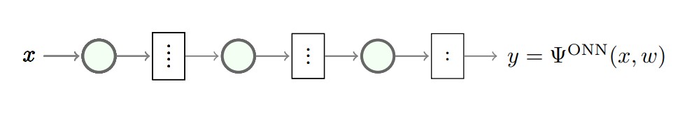
for each hidden layer of the . Here denotes the multivariate normal distribution with mean vector and covariance matrix . More specifically, , and are the covariance matrices associated with weighted addition, application of the activation function, and modulation, respectively. Figure 1 gives a schematic representation of the noise model under study. As we have seen above, in the case we have , otherwise is due to the specific structure of the photonic activation function. The first layer, regardless of an or network, sees a modulated input , i.e., , and afterwards the same steps of weighing and applying an activation function, that is (2). Arguably the hidden layers and their noise structure are the most important parts, especially in deep . Therefore, the main equation governing the behavior of the noise propagation in an will remain (2).
1.3 Noise-resistant designs for
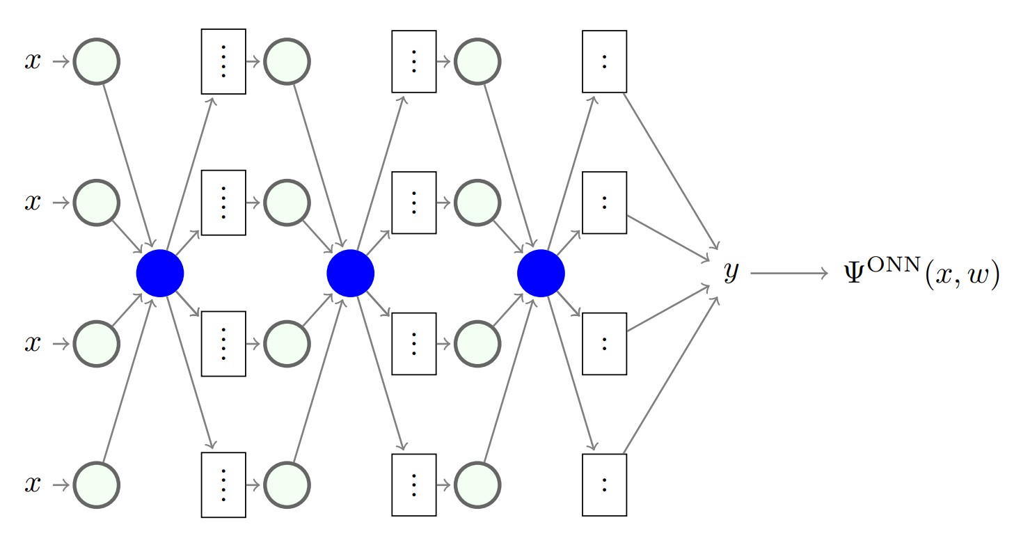
The main contribution of this paper lies in analyzing two noise reduction mechanisms for feed-forward . The mechanisms are derived from the insight that noise can be mitigated through averaging because of the law of large numbers, and they are aimed at using the enormous bandwidth that photonics offer. The first design (Design A) and its analysis are inspired by recent advancements for with random edges in [manita2020universal]; the second design (Design B) is new and simpler to implement, but comes without a theoretical guarantee of correctness for nonlinear , specifically.
Both designs—illustrated in Figure 2—are built from a given for which an optical implementation is desired. Each design proposes a larger by taking parts of the original , and duplicating and arranging them in a certain way. If noise is absent, then this larger produces the same output as the original ; and, if noise is present, then this produces an output closer to the desired than the direct implementation of the as an without modifications would give.
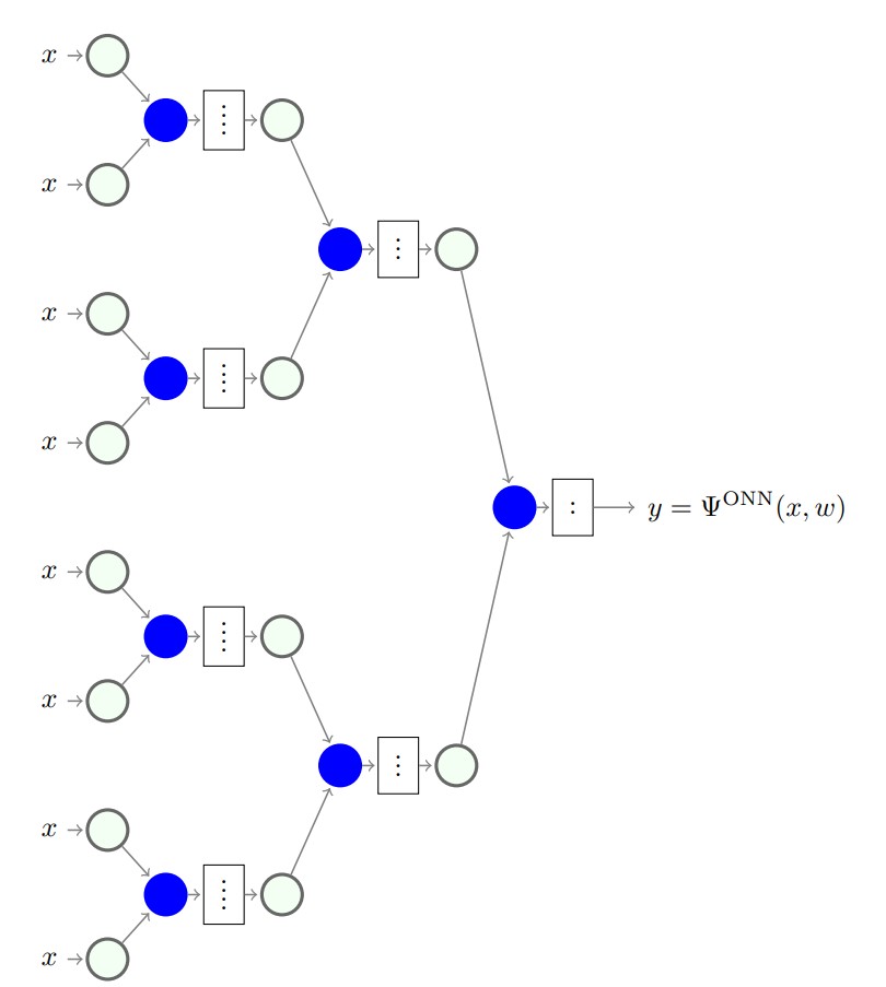
The first mechanism to construct a larger suppressing inherent noise of analog systems starts with a certain number of copies of the input data. The copies are all processed independently by (in parallel arranged copies of) the layers. Each copy of a layer takes in multiple input copies to produce the result of weighted addition, to which the activation mechanism is applied. The copies that are transmitted to each layer (or set of parallel arrayed layers) are independent of each other. The independent outputs function as inputs to the upcoming (copies of the) layers, and so on and so forth.
The idea of the second design is to use multiple copies of the input, on which the weighted addition is performed. The noisy products of the weighted addition are averaged to a single number/light beam. This average is then copied and the multiple copies are fed through the activation function, creating multiple noisy activations to be used as the next layer’s input, and so on.
1.4 Summary of results
Using Design A, we are able to establish that posses the same theoretical properties as . Specifically, we can prove that any