Design of Sn-doped cadmium chalcogenide based monolayers for valleytronics properties
Abstract
Valleytronics, that uses the valley index or valley pseudospin to encode information, has emerged as an interesting field of research in two-dimensional (2D) systems with promising device applications. Spin-orbit coupling (SOC) and inversion symmetry breaking leads to spin-splitting of bands near the energy extrema (valleys). In order to find a new 2D material useful for valleytronics, we have designed hexagonal planar monolayers of cadmium chalcogenides (CdX, X = S, Se, Te) from the (111) surface of bulk CdX zinc blende structure. Band structure study reveals valence band local maxima at symmetry point K and its time reversal conjugate point K. Application of SOC initiates spin-splitting in the valleys that lifts the energy degeneracy and shows strong valley-spin coupling character. We have substituted two Cd atoms in the planar monolayers by Sn atoms which increases the spin-splitting significantly. The structural, dynamic, mechanical and thermal stability of all the monolayers has been confirmed. Values of formation energies indicate that it may be feasible to synthesize the Sn-doped CdSe and CdTe monolayers using bottom-up approach. Zeeman-type spin-splitting is observed in the valley region and Rashba spin-splitting is observed at the point for Sn-doped CdSe and CdTe monolayers. Berry curvature values are more in all the Sn-doped monolayers than the pristine monolayers. These newly designed monolayers are thus found to be suitable for valleytronics applications. Sn-doped monolayers show band inversion deep in the valence and conduction bands between Sn and and X states but lack topological properties.
I Introduction
Two-dimensional (2D) structures form a class of materials which is very much in demand both from fundamental physics point of view and for applications. Since the discovery of graphene monolayer in 2004 [1], 2D material family is increasing with fascinating electronic and spintronic properties. 2D Xene family members are extensively studied but are not stable in their free-standing form without substrates [2, 3, 4]. Transition metal dichalcogenides (TMDs) are another group of 2D family with a graphene-like hexagonal framework and have been realized experimentally [5, 6]. However, these TMDs are layered materials. The minimum possible thickness and wide band gaps of 2D semiconductors make them important in the fields of photovoltaics, sensing, biomedicine, optoelectronics, photocatalysis, etc.
An interesting property seen in 2D materials is valleytronics in which ‘valleys’ are defined as the points in the energy-momentum plots having local minima in conduction band (CB) or local maxima in valence band (VB) [7]. This energy extremum or valley has an intrinsic magnetic moment associated with it as the Bohr magneton is with electron spin, and offers a new degree of freedom of electrons. Similar to the properties like charge and spin, that are used in electronic and spintronic devices, this additional degree of freedom in 2D monolayers with special symmetry, the valley pseudospin, can be used in valleytronic devices. For 2D monolayers with hexagonal lattice, if the band edges are located at the corners of the Brillouin zone (+K and -K points), the existence of two or more degenerate but inequivalent valleys leads to valley physics. The two inequivalent valleys constitute a binary index making the use of valley index as a potential information carrier and has applications in information technology. Due to the large separation of +K and -K (or K) valleys in the momentum space, the valley pseudospin is robust against low-energy phonons and impurity scatterings. Upon breaking space inversion symmetry, the carriers at the valleys are associated with the valley contrasting physical quantities. Valley physics properties are extensively studied in MX2 (M = Mo, W ; X = S, Se, Te) TMDs in their 2D form [8, 9, 10, 11]. The inversion symmetry breaking and strong spin-orbit coupling (SOC) give rise to coupled spin and valley physics in hexagonal monolayers. The spin-valley coupling at the valence-band edges suppresses spin and valley relaxation independently, as flip of spin or valley alone is energetically forbidden by the valley-contrasting spin splitting. Valley Hall and spin Hall effects coexist in both electron-doped and hole-doped systems. These effects suggest the potential of integrated spintronic and valleytronic applications and the necessity and urgency to find and design 2D valleytronic materials with strong spin-valley coupling.
Cadmium chalcogenides CdX (X = S, Se, Te) in their bulk form are well-established wide band gap semiconductors with important applications in photovoltaics and optoelectronic and spintronic devices. Reducing the dimensions from 3D to 2D is expected to result in some exotic electronic and optical properties. 2D honeycomb-like free-standing single to few layered CdX sheets, studied theoretically, indicate that such materials are experimentally achievable [12, 13]. However, there are no reports of synthesis of CdX monolayers experimentally till date. A possible reason is the difficulty to use exfoliation technique since the layers are covalently bonded in the bulk structures. Few reports of synthesis of thick CdSe nanosheets and nanocrystalline Sn-doped CdSe films are available in the literature. Son et al. have used soft template method to synthesize free-standing single layered lamellar-structured CdSe nanosheets with the diffraction pattern showing growth along [000] and [100] axes of hexagonal wurtzite structure [13]. Kaur et al. have prepared Sn-doped CdSe thin films on glass substrate by thermal evaporation which showed characteristic X-ray diffraction peaks of (100) plane of wurtzite structure [14]. They have also concluded from X-ray diffraction studies that Sn2+ ions substitute Cd2+ ions in the CdSe lattice. On the other hand, Sahu et al. found tin-incorporated nanocrystalline CdSe thin films to be along cubic (111) plane [15]. Zinc blende (ZB) (111) plane and wurtzite (W) (001) plane have the same arrangement of atoms except that the stacking of layers is different. Das et al. have prepared thin films of Sn-doped CdS on glass substrate by controlled precipitation of Cd2+ and Sn2+ ions simultaneously and have reported the analysis of the optical data based on Tauc relation [16]. They found that the energy band gap decreased from 2.1 to 1.9 eV and then to 1.85 eV as Sn composition in the solution is increased from 0% to 1% and then to 2%. Planar CdS monolayer is theoretically predicted and is found to be stable [17]. Unsal et al. have explored strain dependent properties of CdTe monolayer and they found -PbO type planar structure of CdTe to be the most stable structure while planar hexagonal CdTe to be dynamically unstable [18]. Zheng et al. have carried out a systematic study of 32 honeycomb monolayer II-VI semiconductors and their heterostructures for potential applications in optoelectronics, spintronics and strong correlated electronics [19]. However, they found the CdX sheets to be poor with respect to dynamic stability. Safari et al. have employed full potential linear augmented plane wave method to study the bonding and optical transitions in planar ZnX and CdX monolayers [20].
Mohanta et al. have used density functional theory (DFT) coupled with semi-classical Boltzmann transport equations, to study the transport properties of CdS and CdSe monolayers and have reported the sheets to be buckled for better stability [21]. Ashwin Kishore et al. have theoretically explored CdX/C2N (X = S, Se) heterostructures as potential photocatalysts for water splitting [22]. Recently Opoku et al. have theoretically examined CdS/SiH heterostructure to study photocatalytic water splitting [23]. Wang et al. have examined the geometric, electronic, optical and potential photocatalytic properties of single-layer CdX (X = S, Se, Te) sheets cleaved from the (001) plane of the bulk wurtzite structure [24]. None of these studies explored the valley physics in these monolayers.
Among all these earlier studies of CdX (X = S, Se, Te), in their 2D hexagonal form, only Zheng et al. and Zhou et al. have carried out comparative studies of CdS, CdSe and CdTe hexagonal monolayers but they did not find all the planar monolayers to be dynamically stable. Our careful optimization and molecular dynamics studies indicate that all the pristine CdX hexagonal monolayers are almost planar and are structurally, dynamically and thermally stable. These are therefore good candidates to explore valley physics.
SOC splits the bands into two spin sub-bands; this splitting is Zeeman-like since the bands are split as if they are subjected to an external magnetic field. Zeeman-type splitting is a consequence of spin discrimination as a result of space inversion symmetry breaking at non-time reversal (non-TR) invariant -points and not due to an intrinsic electric dipole. Moreover, the valley also controls the spin-dependent properties and governs that the valence band maximum (VBM) and conduction band minimum (CBM) must take place at a non-TR -point. The separation of the two spin-split bands at the valleys is termed as valley spin-splitting (VSS). Rashba effect, on the other hand, is spontaneous spin-polarization coupled to the momentum of an electron emerging due to breaking of space inversion symmetry and SOC [25]. This spin degeneracy is lifted for the bands dispersing from the center of the Brillouin zone (BZ) i.e., point or from the points at the BZ boundary, in the wave vector direction and the spin is oriented in a direction perpendicular to both the surface normal and the momentum of the electron. The states exhibiting Rashba splitting consist of mainly p orbitals.
Recent works on suitable materials for spontaneous valley polarization [26], anomalous valley Hall effect [27], strong spin-valley coupling [28], large VSS [29, 30] are worth mentioning and emphasize the need of finding suitable materials for valleytronics applications.
Can SOC initiate VSS in these CdX monolayers, if yes, how strong is VSS? are some of the questions we try to answer in this work. Since SOC strength is very important for significant VSS, we have further doped naturally abundant and nontoxic high Z material, tin, in these monolayers to enhance the effect of SOC. We do find that these Sn-doped CdX monolayers are also structurally, dynamically and thermally stable. We have then studied the electronic structure of all these monolayers to understand the role of SOC to initiate VSS in these Sn-doped CdX monolayers. A comparative study of the electronic band structure of pristine and Sn-doped CdX monolayers brings out the role of Sn and shows that these Sn-doped CdX monolayers show robust spin-valley coupling, larger VSS and Zeeman-like and Rashba splitting, especially in Sn-doped CdTe. Our structural studies involving the cohesive energies reveal that Sn-doped CdX monolayers are more stable than their pristine counterparts. The formation energies indicate that Sn-doped CdX monolayers (in particular, Sn-doped CdTe) are viable in a bottom-up approach. These observations may provide impetus for experimental realization of Sn-doped CdX monolayers.
II Computational Details
We have carried out the electronic structure calculations for the pristine and Sn-doped CdX monolayers within the framework of density functional theory as implemented in Vienna Ab-Initio Simulation Package (VASP) [31, 32]. The ion-electron interaction is described using projected augmented wave method [33]. The exchange-correlation energies of the interacting electrons are considered using Perdew-Burke-Ernzerhof (PBE) generalized gradient approximation (GGA) [34]. The Kohn-Sham wavefunctions are expanded in plane waves with kinetic energy cut-off of 500 eV. The convergence threshold for self-consistent electronic energy calculations is set to 10-6 eV in consecutive iterations. In order to project the DFT wave functions onto the maximally localized Wannier functions, we have used Wannier90 code [35]. PYPROCAR code is used for plotting the band structures [36]. The dynamic stability of the monolayers is established by calculating phonon dispersion using the density functional perturbation theory [37, 38] as implemented in the VASP code along with the PHONOPY package [39]. We have also investigated the thermal stability with ab initio molecular dynamics (AIMD) [40] using Nosé thermostat [41] for NVT ensemble at 300 K. The simulation is carried out for 45 ps with a time step of 3.0 fs Bader charge analysis is carried out to calculate the charge transfer amongst the atoms [42, 43]. The Bader charge for an atom is the difference between the number of its valence electrons and its total charge calculated from the Bader charge analysis. Ionicity of bonds is decided by nonzero Bader charges.
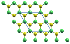
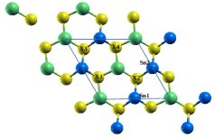
. (a) (b)
. (c) (d)
. (e) (f)
(g)
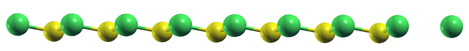
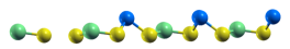
In this work, we have constructed free-standing pristine CdX monolayers from (111) surface of CdX zinc blende (ZB) structure in the -plane as shown in Fig. 1(a). We have then doped Sn in CdX monolayers by substitution at Cd site as shown in Fig. 1(b). It may be noted that the experimental study by Sahu et al. of tin-incorporated nanocrystalline CdSe thin films have reported the structure to be (111) plane of cubic ZB structure [15] and Kaur et al. have observed that Sn2+ ions substitute Cd2+ in the CdSe lattice [14]. A planar unit cell is shown in Fig. 1(a) and Fig. 1(b) for the pristine and Sn-doped monolayers respectively. In order to avoid interaction of the monolayer with its periodic images, we have kept vacuum of minimum 15 Å in the -direction. The self-consistent calculations are performed with mesh of -points using -centered Monkhorst-Pack scheme. All pristine and Sn-doped CdX monolayer structures are fully relaxed using the conjugate gradient method, keeping only the volume of the unit cell constant. All the atoms in the monolayer are allowed to move in any direction and the structure is considered to be optimized when the force on each atom is less than 0.001 eV/Å. After relaxation, a supercell of all the monolayers is used for the calculation of phonon dispersion spectra.
III Results and Discussions
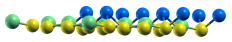
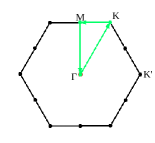
CdX monolayer can be considered to be isovalent with other graphene analogues (leaving the 4 shell of Cd) and therefore honeycomb lattice is a natural choice [12]. The atomic structure of fully relaxed pristine CdX monolayers is almost planar hexagonal as shown in Fig. 1(a), (c) and (e). The lattice parameters obtained after structure optimization are in good agreement with previous calculations [17, 23, 21, 22, 20, 19, 12, 24]. The monolayers exhibit space group P3m1. Fully relaxed structures of Sn-doped CdX monolayers show slight buckling with the Sn atoms coming out of the -plane as shown in Fig. 1(d) and (f). Due to the larger size of the Sn atom in comparison to Cd atom, the buckled structure exhibits a stable structure. The magnitudes of buckling index , along with the lattice constants for pristine and Sn-doped CdX monolayers are listed in Tables S1 and S2 in supplementary information (SI) along with the relevant data available from previous published works on pristine systems. Due to buckling in the -direction, Sn-doped CdX monolayers show reduced hexagonal symmetry with the space group P6m and the lattice parameters in the -plane are reduced in comparison to the respective pristine structures. Such decrease in lattice parameters is reported by Sahu et al. for tin-incorporated CdSe nanocrystalline thin films [15]. Both pristine and Sn-doped monolayers lack inversion symmetry. 2D Brillouin zone, with three high symmetry edge -points, M, K and K, is shown in Fig. 1(g).
The relaxed structures of all the pristine and Sn-doped monolayers are checked for dynamic stability by calculating the phonon band structure (shown in Fig. S1 in SI) and the results do not show signature of any imaginary mode. Zheng et al. [19] and Unsal et al. [18] have studied planar structures of CdX (X = O, S, Se, Te) and CdTe respectively but found that these structures are not dynamically stable. However, we found our almost planar structures to be dynamically stable. There are total 24 branches with 3 acoustic phonon modes and 21 optical phonon modes. The highest phonon frequency decreases as the atomic weight of X atoms increases from S to Te in CdX and Sn-doped CdX monolayers. All the monolayers, studied in this work, satisfy the Born-Huang criteria : and , which indicates the mechanical stability of the monolayers.
Cohesive energy (per atom), as defined in Eqs. (1) and (III), of a monolayer is a measure of binding between the atoms constituting the monolayer and indicates the possibility of monolayer formation if the values are positive. The values of cohesive energy for pristine and for Sn-doped monolayers are tabulated in Table 1 and are indeed found to be positive. Previous results are also quoted for comparison.
| (1) |
and
| (2) | |||
where is the total energy of the isolated atom Y, is the total energy of monolayer consisting of atoms each of Cd and X and is the total energy of above CdX monolayer in which atoms of Cd are replaced by Sn atoms.
| Pristine CdX monolayer | Sn-doped CdX monolayer | |||||
| CdS | CdSe | CdTe | CdS | CdSe | CdTe | |
| or | 2.66 | 2.33 | 2.00 | 3.29 | 2.98 | 2.62 |
| from literature | 2.65a,2.93c | 2.66c | 2.37c | - | - | - |
| 3.5d | 2.99d | 1.90b, 2.45d | ||||
| or | 0.403 | 0.385 | 0.230 | 0.335 | 0.339 | 0.158 |
| 0.233 | 0.231 | 0.228 | - | - | - | |
| from literature | 0.38c, 0.20e, | 0.385c, | 0.366c, | - | - | - |
| 0.54d | 0.21e | 0.18e | ||||
Likewise, cohesive energy of bulk CdX is defined by Eq. (3)
| (3) |
where is the total energy of bulk CdX consisting of atoms each of Cd and X.
Cohesive energy of bulk CdX decreases from S to Te and the same trend is seen in the cohesive energy values for pristine and Sn-doped monolayers. It may be noted that cohesive energy of each Sn-doped monolayer is more than its pristine counterpart by almost 0.6 eV. To understand the reason why it is so, we have compared the difference charge densities (charge density of monolayer - sum of the charge densities of atoms constituting the monolayer)(please refer to SI) of pristine and Sn-doped CdX monolayers. This comparison brings out the changes in bonding on Sn-doping. It is seen that (i) there is more charge build-up between X and Sn atoms in comparison to X and Cd atoms and (ii) there is charge depletion between the two Sn atoms which is absent in pristine structures between two Cd atoms. This results in stronger binding between the atoms in Sn-doped monolayers and hence these monolayers are more stable.
| (4) |
, the difference between cohesive energies of bulk and monolayer, as defined in Eq. (4), is the formation energy per atom (from bulk) and is the cost to be borne to form a 2D structure from the bulk structure [19]. Obviously, cohesive energies of monolayers are smaller than their corresponding bulk structures since the monolayers do not exist naturally. Our values of , as tabulated in Table 1, are less than two-third the values quoted by Zheng et al. [19] indicating that our 2D structures are more stable than those predicted by Zheng et al.. They have obtained CdS monolayer to be planar but CdSe and CdTe to be buckled structures. It may be noted here that Zheng et al. [19] found their 2D CdX structures to be poor with respect to dynamic stability. Dynamic stability of our structures is confirmed and indicates that the 2D structures designed in this work lie at least at a local minimum of potential energy surface rather than at a saddle point [44]. It may be mentioned that formation energy per atom (from bulk) of single layer of ZnO, which has been successfully synthesized [45], has been calculated to be 0.355 eV by Zheng et al. [19]. Our values of are smaller than this value indicating the feasibility of experimental realization of CdX monolayers.
A monolayer, when prepared from its elemental atoms, requires some energy cost, which is quantified as the formation energy by Daguer et al. [46]. The formation energies (per atom) (from constituents) of the pristine and Sn-doped monolayers are defined as
| (5) |
and
| (6) | |||
where and is the total energy per atom of elemental bulk system Y.
The formation energies for all the monolayers, as tabulated in Table 1, are positive indicating that monolayers do not form naturally. However, the monolayer structures have lower formation energy than their bulk structures for pristine materials suggesting their syntheses are feasible. The Sn-doped monolayers have lower formation energy than the corresponding pristine monolayers indicating Sn-doped monolayers can be achieved experimentally. The values of cohesive energies and formation energies, obtained in the present work, are compared with earlier published results whenever available [17, 18, 19, 20, 24] and are in fair agreement as seen in Table 1. Comparing the values of formation energies per atom (from bulk) and (from constituents) for the pristine structures, it is found that the latter is smaller for CdTe monolayer while the values are almost the same for CdSe monolayer and is larger for CdS. Thus, it seems that CdTe monolayer is easy to form from the constituents while CdS monolayer is easier to form from the bulk. Also, the values of are smaller than the corresponding values of , indicating that it may be easier to synthesize the Sn-doped monolayers from the constituents using methods like molecular beam epitaxy, chemical vapour deposition, metallorganic chemical vapor deposition etc.
To investigate the thermal stability of Sn-doped monolayers, molecular dynamics simulations are performed at 300K and the variations in total energy and temperature as a function of time step are shown in Fig. S3 of SI along with the snapshots of the resulting final structures. The plots indicate that the monolayers are thermally stable.
(a) (b) (c)
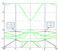
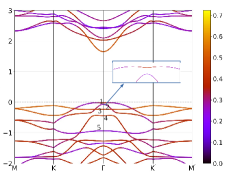
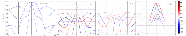
Pristine CdS and CdSe monolayers are direct band gap semiconductors for calculations without and with inclusion of SOC, however CdTe turns into an indirect band gap semiconductor with inclusion of SOC as shown in Fig. 2 (and Fig. S4 in SI). Band gap decreases from CdS to CdTe due to more extended orbitals of the chalcogen atoms in moving from S to Te. The lowest conduction band, formed mainly by the Cd orbitals (hybridized with the chalcogen and orbitals) is also more dispersive. Our calculated band gaps without SOC for pristine monolayers are in good agreement with previous calculations [12, 17, 19, 20, 21, 22, 24] (Please see Table S1 in SI). One Cd atom has three X near-neighbor atoms forming trigonal planar structure. The orbitals of Cd and X atoms split into and components under the crystal field. The valence band (VB) region near the Fermi energy is mainly formed by the X orbitals (the top valence band involves orbitals) hybridized with Cd and orbitals (very small contribution) as revealed from the projected density of states (PDOS) plots depicted in Fig. S5 in SI. The lowest conduction band (CB) is formed by Cd with little contribution of X and orbitals. This is a result of confinement in 2D structures. In bulk CdX, the valence band maximum (VBM) originates purely from X states and conduction band minimum (CBM) is formed by Cd states. The hybridization near VBM is in bulk CdX while it changes to for monolayers. This transition from to results in shortening of Cd-X distance to compensate for the reduced coordination. The CBM has antibonding states of Cd.
All pristine structures do not show band inversion even after inclusion of spin-orbit coupling.
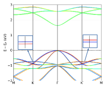
Band degeneracy is lifted with the application of SOC at K and K symmetry points as shown in Fig. 2(a) to (c). The band splitting is very prominent in CdTe monolayer in comparison to CdSe and CdS monolayers. High atomic number of Te results in strong SOC effect, causing prominent band splitting as evident from the band structure plot in Fig. 2(c). Spin-flip at K and K is clearly visible for CdTe and in the insets for CdS and CdSe. This spin-splitting at the valleys with inclusion of SOC in the calculations is called valley spin splitting (VSS). All the pristine monolayers show nice valley-spin coupling at K and K points but the VBM does not occur at K and K points. In order to confirm the spin component at the high symmetry points, we have calculated the expectation values of the spin operators (, and ). The bands at the K and K points arise due to X states and the corresponding component is showing purely and orientations at K and K valleys respectively as revealed in Table S4 in SI. With inclusion of SOC and in presence of inversion asymmetry, the valley degeneracy at K and K points is lifted and the bands are spin-split. This splitting is similar to one observed in magnetic Zeeman effect but occurs in absence of magnetic field. This type of spin-splitting without application of magnetic field is called as Zeeman-type spin-splitting which lifts the out-of-plane spin degeneracy of the top most valence bands at K and K points. Due to the presence of time-reversal symmetry, the spin ordering on splitting is opposite in valleys at K point and its time reversed image point K, as depicted by the colors of the bands in Fig. 2. This shows a strong spin-valley coupling.
(a) (b) (c)
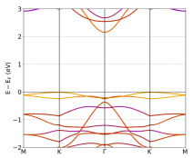
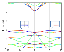
The electronic band structures for Sn-doped CdX monolayers without inclusion of SOC (Fig. 3) reveal that all monolayers are indirect band gap semiconductors with increased band gap values than their pristine counterparts as given in Table S2 in SI. This observation is in contradiction with the experimental band gaps reported in literature [14, 15, 16]. However, the experiments are not for monolayers and have only 2-5 % Sn-doping. The band gaps with inclusion of SOC are slightly less than those without inclusion of SOC. All Sn-doped monolayer systems show band inversion character in the valence band region around point (as seen from the different colors of bands). A specific band inversion is shown in Fig. 3(c) in an enlarged view. This band inversion between two bands 1 and 2 at point is due to and states of Sn and X atoms, while the band inversion between the two bands 4 and 5 at point is due to states of atoms X2 and X3 and states of Sn atoms. (Please refer Fig. 1(b) for the labels of atoms). The PDOS plots shown in Fig. S7 in SI reveal strong hybridization of Sn and states with X states which is responsible for band inversion in all the Sn-doped monolayers.
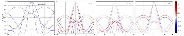
(a) (b) (c)
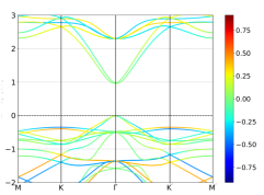
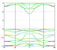
Figure 4 depicts the band structures of Sn-doped CdX monolayers with inclusion of SOC in the calculations. The expectation values of and spin components are same (the roles of up and down spins are flipped) for each monolayer but the expectation value of spin component is different. Therefore, we have shown the , and components for Sn-doped CdS, CdSe and CdTe respectively. Inclusion of spin-orbit coupling lifts the degeneracy of both the valence and the conduction bands near the valleys and the bands are spin-split, the splitting increases from CdS to CdTe. Sn-doped CdS and CdSe monolayers have local minima along with spin-splitting at K and K points in the CB (not visible in Fig. 4 (a)) but these minima lie higher in energy than the CBM at point. Further, the splitting is also very small, we will therefore not discuss the spin-splitting of the conduction band at the valleys.
The spin-splitting in VB is more than that in CB for all the systems. This is because the orbitals participating in the spin-splitting in the valence band region are different from the orbitals in the conduction band region. The K and K valleys show spin-splitting for all the monolayers and presence of time reversal symmetry flips the spins. Figures 2 and 4 nicely depict this split and flip. and M points are the time-reversal symmetry points and the degeneracy of energy bands at these points is protected by the time-reversal symmetry. The maxima in VB do occur at K and K for all the Sn-doped monolayers and they are higher than the value of energy of highest VB at point for Sn-doped CdS and CdSe monolayers as seen in Fig. 4(a) and (b).
The spin-splitting at K and K valleys is again Zeeman-type for all the Sn-doped monolayers like pristine monolayers. The bands are formed by the out-of-plane Sn states and in-plane and out-of-plane states of X2 and X3 chalcogen atoms, as revealed from Table S4 in SI, lifting the spin degeneracy. The magnitude of spin-splitting at K and K points in VB for all the systems are tabulated in Table 2. The spin-splitting in the VB at K and K for CdTe is maximum in the chalcogen series which is quite large and comparable with the reported value for MN2X2 (M = Mo, W; X = F, H) [28] and MoS2 [9].
| CdS | CdSe | CdTe | |
| Pristine | 11.6 | 16.9 | 48.8 |
| Sn-doped | 10.3 | 64.9 | 116.5 |
| – | 2.04 | 1.8 |
(a) (b) (c) (d)
(a) (b) (c) (d)
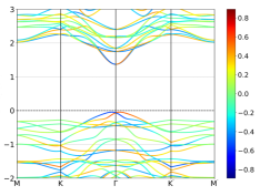
For Sn-doped CdTe monolayer, Rashba spin-splitting is seen at point as shown in Fig. 4(c) and as a result VBM occurs in proximity of point. Rashba spin-splitting is also seen at point for Sn-doped CdSe as shown in Fig. S6(b) in SI. Rashba spin-splitting at point results from the splitting of component of the spin, having the contribution of and states of atoms X1 and X4, lying in the -plane, that lifts the in-plane spin degeneracy. It is known that Rashba splitting normally arises at wave vector with time-reversal symmetry and therefore is likely to occur at point. The Rashba Hamiltonian for 2D free electron gas having inversion asymmetry along , is given by . Here is the Pauli matrix vector and is the Rashba parameter that depends on the atomic number . Rough estimates of from DFT (, where is the change in energy or Rashba energy and is the momentum change or offset) are listed in Table 2 for Sn-doped CdSe and CdTe. Thus, the Rashba spin-splitting lifts the degeneracy in energy as well as momentum and is dependent on the atomic species. The values of , as mentioned in Table 2, are comparable with the value of 1.03 eVÅ for MoTe2 [47].
To understand the role of SOC and Sn-doping in phenomena important for valley physics, we have plotted the valence bands of pristine CdTe and Sn-doped CdTe upto 0.8 eV below the Fermi level in Figs. 5 and 6 respectively. Panel (a) in both the figures depicts the band structures of pristine CdTe and Sn-doped CdTe without the inclusion of SOC (spin-up and spin-down bands are identical) while panels (b), (c) and (d) respectively show the contributions of , and spin components to the bands after inclusion of SOC in the calculations. Site-projected and -decomposed DOS for Te and Sn atoms in pristine and Sn-doped CdTe are plotted in Fig. S10 in SI. It is observed that SOC increases the hybridization of and states of Te with its states and overall the states are broadened in energy extent. Sn-doping enhances these features further due to hybridization of Sn and Te states. As a result of hybridization of Te and Sn states, the energy degeneracies present in the pristine CdTe band structure at , K and K points are lifted on Sn-doping (compare Figs. 5(a) and 6(a)) and the overall nature of band dispersion changes. Inclusion of SOC causes spin-splitting of bands as expected. However, the degeneracy of VBM at point is retained in pristine CdTe after inclusion of SOC, the nature of band dispersion is almost same for up and down spins with spin flipping and more importantly, the contributions of , and components of spins are almost equally visible in the region of interest. Sn-doping significantly changes the band dispersions, more so on inclusion of SOC. The nature of dispersion of up and down spin bands is different and component of spin dominates near point for VBM and the band below it whereas the other two spin components contribute almost in the complete BZ below -0.3 eV. This analysis emphasizes the role of Sn-doping and inclusion of SOC and further can preempt experiments for valley physics.
The Sn and X orbitals hybridize strongly in all Sn-doped CdX monolayers. After substitution of Cd atoms by Sn atoms, small charge asymmetry arises as shown in difference charge density plots (Fig. S9 in SI) and Table S2 of SI. These observations, on inclusion of SOC and inversion asymmetry, show enhanced Zeeman-type spin-splitting in comparison to the respective pristine monolayers at K and K points and Rashba splitting at point in Sn-doped CdSe and CdTe monolayers. Therefore, all the pristine and Sn-doped systems are very promising candidates for valleytronics, both to understand the valley physics and for applications.
(a) (b) (c)
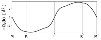
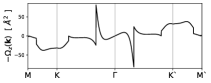
To validate the valley contrasting character, we have calculated the Berry curvature of the Sn-doped monolayers. We employed the Kubo formulation for the calculation of out-of-plane Berry curvature at K and K valleys as given by the following equation: [48, 49].
| (7) |
is the Berry curvature for all the occupied band at wave vector , is the equilibrium Fermi-Dirac distribution function, is the velocity operator along direction, and is the Bloch wave function with eigenvalue . The summation for each is over all the occupied bands. Berry curvature plots in Fig. 7 show equal values with opposite signs at K and K points. Thus we can achieve valley Hall effect by applying in-plane electric field. The carriers near K and K valleys will experience effective magnetic field due to the Berry curvatures leading to anomalous transverse velocity resulting in valley Hall effect. For all the Sn-doped monolayers, we get inequivalent valleys at K and K as the Berry curvature has equal magnitude but opposite signs. The Berry curvature varies inversely with and with the band gap [50]. Therefore, the Berry curvature values are not very large for Sn-doped CdS and CdSe monolayers but for Sn-doped CdTe monolayer, we get spikes, with very large values, in the Berry curvature plot between K (K) and points, in proximity of point.
These spikes are a result of avoided crossing of the hybridized bands that are spin-split due to spin-orbit interaction and orbital hybridization. Sn-doped CdTe, thus, can be a potential candidate for valleytronics, more so with thicker layer and reduced band gap. The Berry curvature values are small for pristine monolayers as compared to Sn-doped monolayers. In case of Sn-doped CdS monolayer, the Berry curvature plot is almost smooth as the SOC effect is very weak and the spin-splitting of bands is small in value. The plot for Sn-doped CdSe does show small kinks near the point due to sizable spin-splitting and spin-flip. Our values of Berry curvature of Sn-doped CdTe monolayer are comparable with those reported by Jena et al. [51] for MoS2 and by Raihan et al. [50] for NbN and TaN.
IV Conclusions
In this study, we have designed a new class of monolayers by doping easily available non-toxic Sn atoms in hexagonal CdX (X = S, Se, Te) monolayers. Our DFT calculations depict two valley points, K and K, with valley spin-splitting in both the VB and CB bands with the application of SOC. The magnitude of valley spin-splitting in VB is large in comparison to CB. Sn atoms do enhance the magnitude of valley spin-splitting. Valleys show Zeeman-type spin-splitting in all the three Sn-doped monolayers while in case of Sn-doped CdSe and CdTe monolayers, Rashba spin-splitting is observed at point which is extremely important for valleytronic and spintronic applications. Spin-valley locking with Zeeman-type splitting and Rashba spin-splitting, due to SOC, are the most flourishing fields of study in valleytronics and spintronics and these properties can be easily harnessed in the semiconducting CdX monolayers by doping environmentally safe and earth-abundant Sn atoms.
Structurally, pristine and Sn-doped CdS monolayers are the most stable but at the same time, the formation energies are also the largest for these monolayers. On the other hand, pristine and Sn-doped CdTe monolayers seem to be energetically realizable from the constituents and due to high Z values experience strong SOC effects resulting in excellent valleytronics properties. Pristine and Sn-doped CdSe also displays good valleytronics properties. Further, thin films and nanosheets of CdSe and nanocrystalline thin films of Sn-doped CdSe have already been synthesized. We therefore foresee good chances of Sn-doped CdSe and CdTe monolayers/nanosheets to be useful in valleytronic and spintronic devices.
This study suggests that theoretically predicted 2D Sn-doped CdX hexagonal monolayers reveal an ideal platform for studying valley physics, Rashba physics, and their integration in valleytronics with spintronics. Our calculations further demonstrate that Sn-doped CdTe can be experimentally synthesized using bottom-up approach.
V Acknowledgements
SC would like to acknowledge financial support from Department of Science and Technology, Government of India through their Women Scientist-A (WOS-A) program. Param Brahma super computer under National Supercomputing Mission established at IISER, Pune has been used for the DFT calculations. This support is gratefully acknowledged. Authors thank Prof. P. Durganandini and Dr. Vikas Kashid for useful discussions.
References
References
- Novoselov et al. [2004] K. S. Novoselov, A. K. Geim, S. V. Morozov, D. Jiang, Y. Zhang, S. V. Dubonos, I. V. Grigorieva, and A. A. Firsov, Science 306, 666 (2004).
- Chiappe et al. [2014] D. Chiappe, E. Scalise, E. Cinquanta, C. Grazianetti, B. van den Broek, M. Fanciulli, M. Houssa, and A. Molle, Adv. Mater. 26, 2096 (2014).
- Dávila et al. [2014] M. E. Dávila, L. Xian, S. Cahangirov, A. Rubio, and G. L. Lay, New J. Phys. 16, 095002 (2014).
- Zhu et al. [2015] F. Zhu, W. Chen, Y. Xu, C. Gao, D. Guan, C. Liu, D. Qian, S. Zhang, and J. Jia, Nature Mater. 14, 1020 (2015).
- Radisavljevic et al. [2011] B. Radisavljevic, A. Radenovic, J. Brivio, V. Giacometti, and A. Kis, Nat. Nanotech. 6, 147 (2011).
- Zhang et al. [2013] Y. Zhang, Y. Zhang, Q. Ji, J. Ju, H. Yuan, J. Shi, T. Gao, D. Ma, M. Liu, Y. Chen, X. Song, H. Y. Hwang, Y. Cui, and Z. Liu, ACS Nano 7, 8963 (2013).
- Rycerz et al. [2007] A. Rycerz, J. Tworzydło, and C. W. J. Beenakker, Nat. Phys. 3, 172 (2007).
- Jiang et al. [2014] T. Jiang, H. Liu, D. Huang, S. Zhang, Y. Li, X. Gong, Y.-R. Shen, W.-T. Liu, and S. Wu, Nat. Nanotech. 9, 825 (2014).
- Kormányos et al. [2013] A. Kormányos, V. Zólyomi, N. D. Drummond, P. Rakyta, G. Burkard, and V. I. Fal’ko, Phys. Rev. B 88, 045416 (2013).
- Manzeli et al. [2017] S. Manzeli, D. Ovchinnikov, D. Pasquier, O. V. Yazyev, and A. Kis, Nat. Rev. Mater. 2, 17033 (2017).
- Srivastava et al. [2015] A. Srivastava, M. Sidler, A. V. Allain, D. S. Lembke, A. Kis, and A. Imamoğlu, Nat. Phys. 11, 141 (2015).
- Zhou et al. [2014] J. Zhou, J. Huang, B. G. Sumpter, P. R. C. Kent, Y. Xie, H. Terrones, and S. C. Smith, J. Phys. Chem. C 118, 16236 (2014).
- Son et al. [2009] J. S. Son, X. D. Wen, J. Joo, J. Chae, S. i. Baek, K. Park, J. H. Kim, K. An, J. H. Yu, S. G. Kwon, S. H. Choi, Z. Wang, Y. W. Kim, Y. Kuk, R. Hoffmann, and T. Hyeon, Ang. Chemie. 48, 6861 (2009).
- Kaur and Tripathi [2016] J. Kaur and S. K. Tripathi, Phil. Mag. 96, 45 (2016).
- Sahu et al. [2018] P. K. Sahu, R. Das, and R. Lalwani, Appl. Phys. A 124, 665 (2018).
- Das and Kumar [2008] R. Das and R. Kumar, J. Mater. Sc. 43, 5972 (2008).
- Garg et al. [2016] P. Garg, S. Kumar, I. Choudhuri, A. Mahata, and B. Pathak, J. Phys. Chem. C 120, 7052 (2016).
- Unsal et al. [2017] E. Unsal, R. T. Senger, and H. Sahin, J. Mater. Chem. C 5, 12249 (2017).
- Zheng et al. [2015] H. Zheng, X.-B. Li, N.-K. Chen, S.-Y. Xie, W. Q. Tian, Y. Chen, H. Xia, S. B. Zhang, and H.-B. Sun, Phys. Rev. B 92, 115307 (2015).
- Safari et al. [2017] M. Safari, Z. Izadi, J. Jalilian, I. Ahmad, and S. Jalali-Asadabadi, Phys. Lett. A 381, 663 (2017).
- Mohanta et al. [2020] M. K. Mohanta, A. Rawat, N. Jena, R. Ahammed, and A. De Sarkar, J. Phys.: Conden. Matt. 35, 355301 (2020).
- Ashwin Kishore et al. [2020] M. R. Ashwin Kishore, K. Larsson, and P. Ravindran, ACS Omega 5, 23762 (2020).
- Opoku et al. [2022] F. Opoku, A. Aniagyei, O. Akoto, E. E. Kwaansa-Ansah, N. K. Asare-Donkor, and A. A. Adimado, Mater. Adv. 3, 4629 (2022).
- Wang et al. [2016] J. Wang, J. Meng, Q. Li, and J. Yang, Phys. Chem. Chem. Phys. 18, 17029 (2016).
- Bychkov and Rashba [1984] Y. A. Bychkov and É. I. Rashba, Sov. J. Exp. Theo. Phys. Lett. 39, 78 (1984).
- Zhao et al. [2019] P. Zhao, Y. Ma, C. Lei, H. Wang, B. Huang, and Y. Dai, Appl. Phys. Lett. 115, 261605 (2019).
- Peng et al. [2020] R. Peng, Y. Ma, X. Xu, Z. He, B. Huang, and Y. Dai, Phys. Rev. B 102, 035412 (2020).
- Dou et al. [2020] K. Dou, Y. Ma, R. Peng, W. Du, B. Huang, and Y. Dai, Appl. Phys. Lett. 117, 172405 (2020).
- Zang et al. [2021] Y. Zang, Y. Ma, R. Peng, H. Wang, B. Huang, and Y. Dai, Nano Res. 14, 34 (2021).
- Ai et al. [2021] H. Ai, D. Liu, J. Geng, S. Wang, K. H. Lo, and H. Pan, Phys. Chem. Chem. Phys. 23, 3144 (2021).
- Kresse and Furthmüller [1996] G. Kresse and J. Furthmüller, Phys. Rev. B 54, 11169 (1996).
- Kresse and Furthmüller [1996] G. Kresse and J. Furthmüller, Comput. Mater. Sci. 6, 15 (1996).
- Blöchl [1994] P. E. Blöchl, Phys. Rev. B 50, 17953 (1994).
- Perdew et al. [1996] J. P. Perdew, K. Burke, and M. Ernzerhof, Phys. Rev. Lett. 77, 3865 (1996).
- Mostofi et al. [2014] A. A. Mostofi, J. R. Yates, G. Pizzi, Y.-S. Lee, I. Souza, D. Vanderbilt, and N. Marzari, Comp. Phys. Commun. 185, 2309 (2014).
- Herath et al. [2020] U. Herath, P. Tavadze, X. He, E. Bousquet, S. Singh, F. Muñoz, and A. H. Romero, Comp. Phys. Commun. 251, 107080 (2020).
- Baroni et al. [1987] S. Baroni, P. Giannozzi, and A. Testa, Phys. Rev. Lett. 58, 1861 (1987).
- Gonze [1995] X. Gonze, Phys. Rev. A 52, 1096 (1995).
- Togo et al. [2008] A. Togo, F. Oba, and I. Tanaka, Phys. Rev. B 78, 134106 (2008).
- Anglada et al. [2003] E. Anglada, J. Junquera, and J. M. Soler, Phys. Rev. E 68, 055701 (2003).
- Nosé [1984] S. Nosé, J.Chem. Phys. 81, 511 (1984).
- Tang et al. [2009] W. Tang, E. Sanville, and G. Henkelman, J. Phys.: Conden. Matt. 21, 084204 (2009).
- Bader [1990] R. F. W. Bader, Atoms in molecules : a quantum theory (Oxford : Clarendon press, 1990).
- Zhuang and Hennig [2014] H. L. Zhuang and R. G. Hennig, JOM 66, 366 (2014).
- Tusche et al. [2007] C. Tusche, H. L. Meyerheim, and J. Kirschner, Phys. Rev. Lett. 99, 026102 (2007).
- Daguer et al. [2021] S. C. Daguer, N. D. L. Espriella, and C. O. López, J. Phys.: Conf. Ser. 2046, 012037 (2021).
- Gupta and Yakobson [2021] S. Gupta and B. I. Yakobson, J. Am. Chem. Soc. 143, 3503 (2021).
- Thouless et al. [1982] D. J. Thouless, M. Kohmoto, M. P. Nightingale, and M. den Nijs, Phys. Rev. Lett. 49, 405 (1982).
- Yao et al. [2004] Y. Yao, L. Kleinman, A. H. MacDonald, J. Sinova, T. Jungwirth, D. S. Wang, E. Wang, and Q. Niu, Phys. Rev. Lett. 92, 037204 (2004).
- Ahammed and De Sarkar [2022] R. Ahammed and A. De Sarkar, Phys. Rev. B 105, 045426 (2022).
- Jena et al. [2019] N. Jena, Dimple, R. Ahammed, A. Rawat, M. K. Mohanta, and A. De Sarkar, Phys. Rev. B 100, 165413 (2019).