Nature of the current-induced insulator-to-metal transition
in Ca2RuO4 as revealed by transport-ARPES
The Mott insulator Ca2RuO4 exhibits a rare insulator-to-metal transition (IMT) induced by DC current 1. While structural changes associated with this transition have been tracked by neutron diffraction, Raman scattering, and x-ray spectroscopy, work on elucidating the response of the electronic degrees of freedom is still in progress 2; 3; 4; 5. Here we unveil the current-induced modifications of the electronic states of Ca2RuO4 by employing angle-resolved photoemission spectroscopy (ARPES) in conjunction with four-probe transport. Two main effects emerge: a clear reduction of the Mott gap and a modification in the dispersion of the Ru-bands. The changes in dispersion occur exclusively along the high-symmetry direction, parallel to the -axis where the greatest in-plane lattice change occurs. These experimental observations are reflected in dynamical mean-field theory (DMFT) calculations simulated exclusively from the current-induced lattice constants, indicating a current driven structural transition as the primary mechanism of the IMT. Furthermore, we demonstrate this phase is distinct from the high-temperature zero-current metallic phase. Our results provide insight into the elusive nature of the current-induced IMT of Ca2RuO4 and advance the challenging, yet powerful, technique of transport-ARPES.
Ca2RuO4 (CRO) is a quasi-two-dimensional system comprising of layers of RuO6 octahedra that undergo an insulator-to-metal transition (IMT) when heated above K 6; 7. The low temperature insulating (high temperature metallic) phase is commonly referred to as S-phase (L-phase), due to the shorter (longer) -axis. At low temperatures, the -axis compression tilts and distorts the RuO6 octahedra, lifting the electron degeneracy of the Ru states, and inducing a Mott-insulating gap 8. This sensitivity of the ground state to the octahedral compression renders the system extremely prone to external perturbation. Aside from temperature, the IMT can also be tuned through chemical substitution 9; 10, pressure 11; 12, epitaxial strain 13, electric fields 14, and interestingly, the aforementioned DC current 1. In the latter case, the metallic phase persists so long as current is continuously passed through the sample, making it a rare example of a long-lasting steady state in a field of non-equilibrium physics dominated by pump-probe techniques 15; 16.
While the zero-current IMT is understood as a consequence of the shortened -axis, the mechanism by which the current induces the IMT is not established. The current-induced structural changes are distinct from those driven by temperature, with the insulating (metallic) state exhibiting a slightly larger (smaller) -axis compared to the zero-current counterparts, earning the S* and L* denominations, respectively. The current also suppresses the antiferromagnetic order that typically occurs below = 110 K. While this IMT is observed regardless of whether the current is applied within the -plane 3; 17; 18 or along the -axis 2, an unusual metal-insulator nanostripe pattern arises when intermediate current densities are applied exclusively parallel to the -axis of the crystal 18.
In order to pinpoint the mechanism behind the current-driven IMT in CRO, an understanding of the electronic structure evolution between the insulating and current-driven steady states are essential. Here, we combine transport with angle-resolved photoemission spectroscopy (transport-ARPES) to directly probe the electronic structure under current. Both transport and ARPES probe scattering processes and density of states; however, transport is an integrative probe over the whole sample, whereas ARPES can probe the state of the system point-by-point within the spatial resolution of the beamspot. The merging of an ‘integrative’ with a ‘scanning’ probe allows us to better differentiate between crystal defects and intrinsic microscale phenomena. Although transport-ARPES has the potential to study the effects of current on phase transitions 19, superconductivity 20; 21, charge density waves 22, and competing orders in strongly correlated systems 23, its wide application has to date, been precluded by the complexity of dissociating real current-driven changes from the effects of the stray electric and magnetic fields generated by the current 21; 24; 25; 26; 5.
We mitigate these challenges by using a micron-size beamspot in conjunction with core-level spectroscopy to establish a common binding energy reference at different magnitudes of applied current (Fig. 1). This approach uncovers clear signatures of the current-induced IMT in the electronic structure of CRO: a global reduction of the charge gap (Fig. 2) and a change in the low-energy Ru-bands at the edge of the Brillouin zone (Fig. 3). These changes in dispersion occur exclusively parallel to the axis that undergoes a larger structural modification under current, suggesting that the current prompts a structural change, which is the main driver of the IMT. Additionally, we find the resulting Fermi surface to be distinct from that of the high temperature phase, indicating that the current-induced phase is not simply a consequence of Joule heating (Fig. 4h).
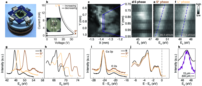
Our transport-ARPES experimental configuration is presented in Fig. 1a, along with the characteristic - curve in Fig. 1b. The distinctive negative differential resistance of the current-induced transition 18; 4 indicates a high quality sample devoid of large cracks or deformations that would globally impede current flow 17. To avoid possible domain formation, such as the metal-insulator nanostripe pattern found at intermediate current densities 18, we refer to the current-voltage characteristic to ensure that the magnitude of the applied current is large enough such that the whole sample has completely transitioned into the L*-phase. This critical current will depend on the dimensions of the particular sample and the temperature at which the experiment is carried out 17.
Before presenting the transport-ARPES results on CRO, we briefly discuss our experimental strategy to address the effects of the stray electric and magnetic fields generated by an electric current passed through the sample (Supplementary section B). The magnetic field results in a rigid momentum shift and deformation of the measured band structure. The latter has minimal impact in our experiment, whereas the former is accounted for by setting the high symmetry points of the measured spectra to their established positions in k-space (Fig. C7). On the other hand, the potential gradient that develops across the sample as a consequence of current flow causes a deviation in energy and broadens spectral features. This gradient shifts the kinetic energy of emitted photoelectrons by the magnitude of the local potential at the emission position 27. We illustrate this in Figs. 1(d-f) by tracking the Ca core level binding energy; the peak shifts as the beam is physically moved along the direction of current flow. Note that the S*-phase exhibits a larger shift, demonstrating that it experiences a larger local electric field, than the L*-phase at higher current [Figs. 1(e, f)], consistent with the negative differential resistance of the current-induced IMT. The slope of the spatial variation of the core level illustrates the average field present across that particular sample region. The presence of smooth slopes indicates which regions have homogeneous current flow suitable for ARPES measurement, in contrast to regions compromised by impurities or cracks within the crystal.
While changes in the low-energy electronic states are expected to occur due to the IMT, core levels will be significantly less affected. As neither the core level lineshapes, nor the Ca -O energy difference changes evidently across the IMT (Fig. 1i), we conclude that the dominant cause of the energy shift is the electrostatic potential, rather than chemical shifts, within a small uncertainty of order meV [Supplementary section B]. Such small chemical shifts would not affect the main conclusions discussed below. This allows us to apply the extracted core level shifts of 4.5 eV between the S- and S*-phases, and 1.6 eV between the S- and L*-phases, to the valence band spectra obtained at the same spot on the sample to expose the intrinsic current-induced modifications (Fig. 1h, j).
In addition, since photoemission data are simultaneously acquired over the area illuminated by a finite sized beam spot, photoelectrons experience a range of energy shifts given by the potential gradient across the spot, as seen in (Fig. 1k). To minimize this range and enable the observation of band shifts on the order of the insulating gap in CRO ( eV 9), we use a 15 m diameter spot. This results in a current-induced broadening of meV (Supplementary section B), which allows us to probe the intrinsic L*-phase electronic signatures discussed in the following sections. Once the effects of the current-induced stray fields are accounted for, we uncover the IMT-driven modifications of the valence band as the system transitions from the S- to L*-phase. Note, despite the crystal structure decreasing in orthorhombicity as it goes through the IMT, high symmetry points are denoted with respect to the orthorhombic Brillouin zone.
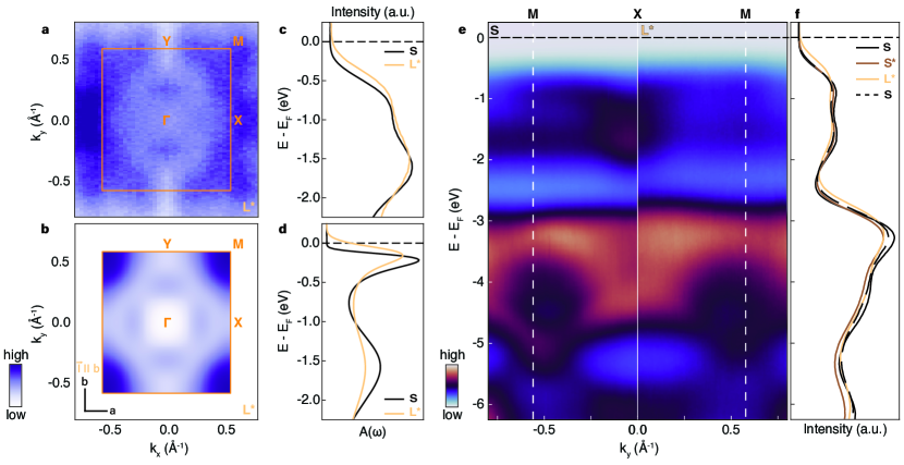
Fermi surfaces in the current-induced metallic L*-phase obtained from ARPES and DMFT are presented in Figs. 2a and b. While the charge gap removes spectral weight at the Fermi level in the insulating S-phase, with applied current we clearly detect spectral weight at (Fig. 2a). Indeed, a reduction of the total gap in CRO emerges when the spectral weight integrated over the whole Brillouin zone between the S- and L*-phases is compared (Fig. 2c), as also recently observed by Curcio et. al 5. This is further illustrated by the ARPES maps acquired along in the two phases (Fig. 2e), and by the evolution of the energy distribution curves (EDCs) integrated over the orthorhombic Brillouin zone edge for zero, intermediate, and high current (Fig. 2f). We emphasize that the gap reduction occurs only when the IMT is fully crossed (brown to yellow curves) and is accompanied by a redistribution of the spectral weight towards lower binding energies for the whole Ru and O valence band manifold. These observations are in good agreement with the metallic Fermi surface and momentum integrated spectral function obtained by DMFT calculations (Figs. 2b and d), in which the current is accounted for through the use of the current-induced lattice constants obtained by neutron diffraction 2.
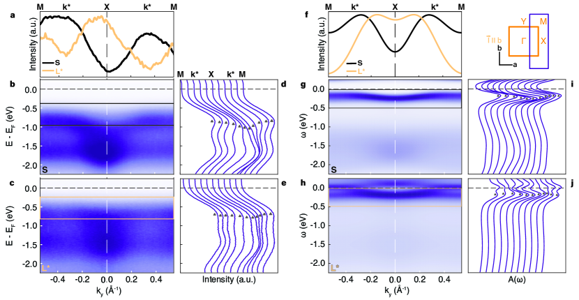
While no noticeable differences are observed in the dispersion of the O-bands (Fig. 2e), the dispersion of the Ru-bands undergoes a distinct change through the IMT (Fig. 3). Without current, flat bands around Å-1 are observed to disperse downwards into the point, and all bands are found well below , consistent with the insulating phase (Fig. 3b). Upon applying current, two main changes occur (Fig. 3c): the spectral weight at the point close to the Fermi level increases, whereas the spectral weight at decreases. These effects are further illustrated by the momentum distribution curves (MDCs) shown in Fig. 3a. While a trough at is enveloped by two peaks at in the zero-current MDC, a peak is enveloped by two troughs in the current-induced MDC. Similarly, while the cascade of EDCs in Fig. 3d exhibits a clear modulation of spectral weight across the cut, the EDCs of the L*-phase in Fig. 3e are fairly momentum independent. These changes were not observed by Curcio et. al 5, possibly due to the fact that these bands are only visible at specific kz values (Supplementary section A).
We compare our transport-ARPES results to DMFT calculations (Fig. 3f-j). As the band disperses from to in the insulating S-phase (Fig. 3g), it flattens out before reaching the Fermi level, consistent with experimental observations (Fig. 3b) and other DMFT calculations 8. In the L*-phase (Fig. 3h), the band is seen to cross the Fermi level before flattening in the unoccupied region of the spectrum around the point. Although unoccupied states cannot be resolved with standard ARPES, the depletion of spectral weight experimentally observed at is consistent with the scenario sketched by DMFT. Aside from the difference in distribution of spectral weight between the lower and upper Ru bands, the calculated S-phase MDC (Fig. 3f) agrees well with the experiment. While the agreement seems poor for the L*-phase, the increase in intensity at is still present. The cascade of calculated EDCs (Fig. 3i, j) also show the modulation of spectral weight across the cut in the S-phase and the momentum independent shape of the spectral weight in the L*-phase, similar to that observed in the experiment (Fig. 3d, e). Since the DMFT results only incorporate the current through the use of the current-induced lattice structure, the general similarity in the evolution of the Ru-states between the ARPES data and DMFT calculations hints toward a current-induced structural effect as the underlying driving mechanism for the IMT. To verify this, we measure the dispersion at the perpendicular Brillouin zone edge, along .
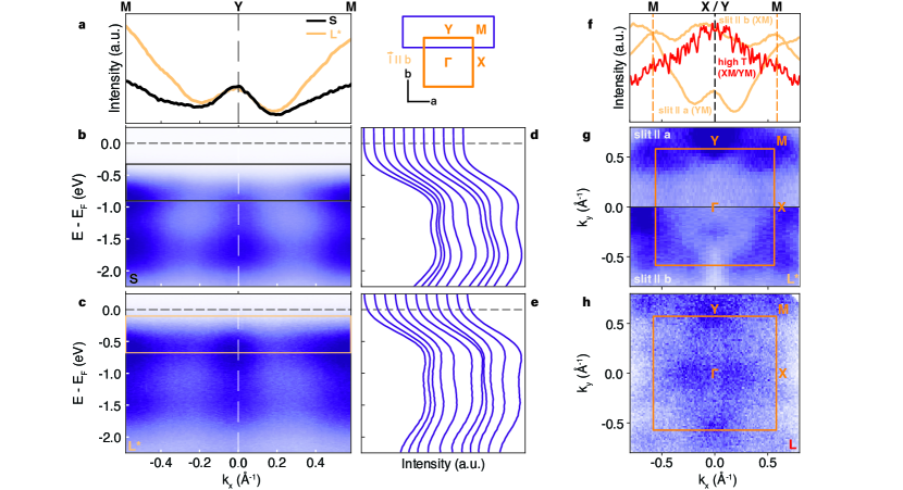
Data displayed in Fig. 3 are measured with the analyser slit along the crystallographic -axis; to observe the cut, we rotate the crystal by 90∘ to align the analyser slit along the -axis. This allows the photoemission matrix element to access different orbital symmetries, while maintaining -polarized light, resulting in the Fermi surface displayed in the top half of Fig. 4g (the bottom half of the figure is taken from Fig. 2a to present the complete polarization-dependent L* Fermi surface for comparison). No significant dispersion is found along the cut, as shown in Fig. 4b, with spectral weight being most concentrated at the and points. Comparing Figs. 3b with 4b, we see the S-phase is quite anisotropic between the and directions. However, the and dispersions computed by DMFT are nearly indistinguishable despite including the orthorhombic asymmetry (Supplementary Section C), suggesting that there exist underlying correlation effects, even in the zero-current low-temperature Mott phase, which have yet to be accounted for.
Intriguingly, no visible modification of the Ru dispersion occurs along across the IMT (Fig. 4b, c), aside from a redistribution of spectral weight from the higher to lower energy Ru-band. This is highlighted by the consistent shape of the MDCs (Fig. 4a) and EDCs (Fig. 4d, e), in striking contrast to the changes observed along the direction (Fig. 3a - e). This contrast in the electronic structure evolution across the IMT along the two high-symmetry directions can be attributed to a smaller corresponding change in lattice constant along the -axis, = 0.04 Å, as compared to the -axis, = 0.2 Å 2. In fact, the measured dispersion in the L*-phase (Fig. 3c) more closely resembles the dispersion (Fig. 4c); in other words, the L*-phase is more isotropic. Therefore, our results suggest that the decreased orthorhombicity of the lattice is the primary driver of the band structure evolution, in strong agreement with Bertinshaw et al 2.
Finally, let us comment on the role of Joule heating in this current-induced IMT, which is heavily discussed in the literature 1; 3; 17. To gain further insight, particularly from an electronic structure perspective, we compare the transport-ARPES data in the current-induced metallic L*-phase for both analyser slit orientations (Fig. 4g) with zero-current ARPES data on the high-temperature metallic L-phase (Fig. 4h). All experimental conditions (i.e. light polarization, photon energy, etc.) remain the same between the two measurements, aside from the temperature ( = 180 K and 384 K, respectively). While the Fermi surface characteristics of the L*-phase exhibit a clear dependence on experimental geometry, the L-phase Fermi surface shows the same spectral features (within the limits of thermal broadening), when measured along both in-plane axes (Fig. F9). This indicates a much smaller orthorhombic distortion of the crystal at high temperatures, in accordance with the further reduced orthorhombicity of the L-phase compared with the L*-phase 10. The differences in the Fermi surfaces are further highlighted by the MDCs taken at the edge of the BZ (Fig. 4f), where significant intensity is found at the points for the L*-phases (yellow), while intensity peaks in the center of the high-temperature L-phase curve and progressively drops off towards the edges of the Brillouin zone (red). These differences confirm that the current-induced L*-phase is indeed a unique state rather than a consequence of Joule heating and that the underlying physics of the two phases must be electronically different.
Discussion
We have unveiled the current-induced electronic band structure of CRO using the powerful method of transport-ARPES (ARPES conducted in a four-point transport configuration). By establishing core levels as a reference point for energy shifts due to stray electric fields, we have demonstrated the reduction of the gap through the IMT. We have also observed a change in the dispersion of the Ru band, occurring only along the direction, i.e. parallel to the -axis and along the direction of current flow. We point out that the current-induced nanostripe pattern also only manifests when the current is applied parallel to the -axis 18, emphasizing the strong relationship between the DC current and lattice. Furthermore, we have determined the nature of the current-induced metallic L*-phase to be electronically distinct from the temperature-driven metallic L-phase, confirming that the former is indeed a unique state. Although the question by what mechanism the current affects the lattice structure still remains, our results will motivate further theoretical investigations of the current-induced IMT in CRO; this will likely require the explicit inclusion of a non-equilibrium component representing the current. Furthermore, our results will spark the investigation of current-induced phase transitions with transport-ARPES in many other complex oxides.
Methods
Experimental
High-quality single crystals of Ca2RuO4 were grown using the optical floating zone technique as described in Ref. 28. Samples were characterized with x-ray Laue diffraction equipped with a tungsten source and a MWL120 Real-Time Back-Reflection Laue camera, as well as with magnetometry measured in a Quantum design MPMS SQUID to confirm = 110 K and no impurities from additional phases were present. The crystals are shaped with a diamond wire saw to an average dimension of approximately 2 x 1 x 0.25 mm3. Sculpting the crystals into a simple rectangular shape is essential to provide the current with a more homogeneous and efficient path. Characterizing ARPES measurements in the zero-current S-phase were conducted at the Quantum Materials Spectroscopy Centre beamline at the Canadian Light Source using a horizontal electron analyser slit geometry. The crystals were cleaved in-situ at 6 10-11 mbar using a ceramic top post. Spectra were measured at 74 eV with - and -polarized light at K to avoid charging.
Transport-ARPES experiments were carried out at the MAESTRO beamline (7.0.2) at the Advanced Light Source at Lawrence Berkeley National Lab using a horizontal electron analyser slit geometry. The crystals were cleaved in-situ at 1.7 10-11 mbar using a ceramic top post. Spectra were measured at 74 eV with - and -polarized light. Current was applied parallel to the -axis in a four-probe configuration using a Keithley 2400 Source Measure Unit. Before the start of measurements, the ground was confirmed to be the same as that of the electron analyser. The samples were kept at = 180 K under constant cooling to prevent Joule heating. High temperature ARPES experiments were also carried out at MAESTRO at = 380 K. The manipulator was heated from 10 K, and following heating the manipulator position was allowed to settle for 4 h. Samples were cleaved in-situ at 2 10-10 mbar using a ceramic top post.
To mount and prepare the samples for transport-ARPES measurements at MAESTRO, conductive EPO-TEK H20E epoxy was used to glue five 75 m gold wires to the crystal and attach the wires to the gold plate contacts of the chip carrier. Insulating and thermally efficient Loctite Stycast 2850FT with catalyst 24LV is then used to glue the crystal, wire-side down, onto a sapphire substrate. Both epoxies are thermally efficient and were cured just below 80 ∘C for over 4 hours. The substrate prevents the crystal from making contact with the gold base of the chip carrier. It is also important to glue the contacted face of the crystal to the substrate as the wires must be secure during the crystal cleave. The chip carrier can then be placed on the custom-made transport pucks of the MAESTRO beamline, shown in Fig. 1a, which feature eight primary contacts made of gold-coated beryllium copper and secured with titanium screws and molybdenum nuts. Phosphor bronze clips are used to hold the chip carrier in place. The puck itself is made of oxygen-free copper and has a protruding piece at the center, hugged by the ceramic frame, to ensure strong thermal coupling with the sample.
DFT + DMFT band structure calculations.
Our (single-shot) DFT+DMFT calculations were performed using the cristallographically refined atomic coordinates for the S-, S*-, L*- and L-phases, as obtained from neutron diffraction.
After convergence of the DFT calculation for each of these structures (using the VASP code 29 with a full potential linearized augmented plane-wave method and PBE-GGA exchange-correlation functional), we downfolded the Kohn-Sham wavefunctions to an effective Wannier basis 30 covering an energy window of eV to eV around the Fermi level . The resulting three band model originates from the cubic Ru states and includes: i) non-cubic crystal field distortions, as well as ii) the spin-orbit coupling operator projected to the states.
The interaction is approximated by the rotationally invariant Kanamori operator with a Hubbard eV and Hund’s coupling eV (following Kim et al. 31) for all structures. For the solution of the DMFT auxiliary impurity models, we employ the continuous-time hybridization-expansion quantum Monte-Carlo solver (CT-QMC) of the TRIQS library 32; 33.
After DMFT convergence we performed analytical continuation of the self-energy by maximum-entropy method (MaxEnt) following Kraberger et al. 34. The resulting real-frequency self-energies were then used to produce the orbitally- and momentum-resolved single-particle spectral functions which are shown in this work.
Comprehensive technical details and plots (e.g. of the analytically continued self-energies) can be found in the supplemental material of Ref. 2.
Acknowledgments
We acknowledge useful discussions with Jan Bruin, Stephanie Gilbert-Corder, Christopher Gutiérrez, Sae-Hee Ryu, Henri Menke, Nobumichi Tamura, and Giorgio Levy, as well as MengXing Na and Alex Anees for figure design. This research was undertaken thanks in part to funding from the Max Planck-UBC-UTokyo Centre for Quantum Materials and the Canada First Research Excellence Fund, Quantum Materials and Future Technologies Program. This project is also funded by the Killam, Alfred P. Sloan, and Natural Sciences and Engineering Research Council of Canada’s (NSERC’s) Steacie Memorial Fellowships (A.D.); the Alexander von Humboldt Foundation (A.D.); the Canada Research Chairs Program (A.D.); NSERC, Canada Foundation for Innovation (CFI); the Department of National Defence (DND); the British Columbia Knowledge Development Fund (BCKDF); the Mitacs Accelerate Program; the QuantEmX Program of the Institute for Complex Adaptive Matter (ICAM); the Moore EPiQS Program (A.D.); and the CIFAR Quantum Materials Program (A.D.). Use of Advanced Light Source (MAESTRO beamline) at Lawrence Berkeley National Lab is supported by the U.S. Department of Energy, Office of Science User Facility under Contract No. DE-AC02-05CH11231. Use of the Canadian Light Source (Quantum Materials Spectroscopy Centre), a national research facility of the University of Saskatchewan, is supported by CFI, the NSERC, the National Research Council, the Canadian Institutes of Health Research, the Government of Saskatchewan, and the University of Saskatchewan. C.T.S. acknowledges student support from the NSERC and the Advanced Light Source.
Conflict of interest
The authors declare no competing interests.
Availability of data and materials
All relevant data and supplementary information are available from the corresponding author upon request.
Author contributions
C.T.S., B.K., E.R. and A.D. conceived the project and designed the experiments. M.K. grew the crystals and C.T.S and P.P. characterized them. C.T.S., I.M, M.Z, N.-H.J., S.Z., S.S, C.A-Y., V.Z., and B.Z. carried out the ARPES experiments with assistance from S.G., C.J., A.B. and E.R.. C.T.S. performed the data analysis and I.M., M.Z., S.Z, N.-H.J., I.S.E, C.J., A.B., E.R., and A.D. provided input and assistance. M.S. and P.H. conducted and analysed the DFT and DMFT calculations. C.T.S wrote the manuscript with significant input from I.M. and M.Z. and input from all authors. B.K and A.D. were responsible for the overall direction, planning, and management of the project.
References
- Okazaki et al. (2013) R. Okazaki, Y. Nishina, Y. Yasui, F. Nakamura, T. Suzuki, and I. Terasaki, Journal of the Physical Society of Japan 82, 103702 (2013).
- Bertinshaw et al. (2019) J. Bertinshaw, N. Gurung, P. Jorba, H. Liu, M. Schmid, D. T. Mantadakis, M. Daghofer, M. Krautloher, A. Jain, G. H. Ryu, O. Fabelo, P. Hansmann, G. Khaliullin, C. Pfleiderer, B. Keimer, and B. J. Kim, Phys. Rev. Lett. 123, 137204 (2019).
- Fürsich et al. (2019) K. Fürsich, J. Bertinshaw, P. Butler, M. Krautloher, M. Minola, and B. Keimer, Phys. Rev. B 100, 081101 (2019).
- Jenni et al. (2020) K. Jenni, F. Wirth, K. Dietrich, L. Berger, Y. Sidis, S. Kunkemöller, C. P. Grams, D. I. Khomskii, J. Hemberger, and M. Braden, Phys. Rev. Materials 4, 085001 (2020).
- Curcio et al. (2023) D. Curcio, C. E. Sanders, A. Chikina, H. E. Lund, M. Bianchi, V. Granata, M. Cannavacciuolo, G. Cuono, C. Autieri, F. Forte, A. Romano, P. D. Cuoco, J. Avila, C. Polley, T. Balasubramanian, R. Fittipaldi, A. Vecchione, and P. Hofmann, arXiv preprint arXiv:2303.00662 (2023).
- Braden et al. (1998) M. Braden, G. André, S. Nakatsuji, and Y. Maeno, Phys. Rev. B 58, 847 (1998).
- Alexander et al. (1999) C. S. Alexander, G. Cao, V. Dobrosavljevic, S. McCall, J. E. Crow, E. Lochner, and R. P. Guertin, Phys. Rev. B 60, R8422 (1999).
- Gorelov et al. (2010) E. Gorelov, M. Karolak, T. O. Wehling, F. Lechermann, A. I. Lichtenstein, and E. Pavarini, Phys. Rev. Lett. 104, 226401 (2010).
- Nakatsuji and Maeno (2000) S. Nakatsuji and Y. Maeno, Phys. Rev. Lett. 84, 2666 (2000).
- Friedt et al. (2001) O. Friedt, M. Braden, G. André, P. Adelmann, S. Nakatsuji, and Y. Maeno, Phys. Rev. B 63, 174432 (2001).
- Nakamura et al. (2002) F. Nakamura, T. Goko, M. Ito, T. Fujita, S. Nakatsuji, H. Fukazawa, Y. Maeno, P. Alireza, D. Forsythe, and S. Julian, Phys. Rev. B 65, 220402 (2002).
- Steffens et al. (2005) P. Steffens, O. Friedt, P. Alireza, W. G. Marshall, W. Schmidt, F. Nakamura, S. Nakatsuji, Y. Maeno, R. Lengsdorf, M. M. Abd-Elmeguid, and M. Braden, Phys. Rev. B 72, 094104 (2005).
- Dietl et al. (2018) C. Dietl, S. K. Sinha, G. Christiani, Y. Khaydukov, T. Keller, D. Putzky, S. Ibrahimkutty, P. Wochner, G. Logvenov, P. A. van Aken, B. J. Kim, and B. Keimer, Applied Physics Letters 112, 031902 (2018).
- Nakamura et al. (2013) F. Nakamura, M. Sakaki, Y. Yamanaka, S. Tamaru, T. Suzuki, and Y. Maeno, Scientific Reports 3, 2536 (2013).
- Zonno et al. (2021) M. Zonno, F. Boschini, and A. Damascelli, Journal of Electron Spectroscopy and Related Phenomena 251, 147091 (2021).
- Giannetti et al. (2016) C. Giannetti, M. Capone, D. Fausti, M. Fabrizio, F. Parmigiani, and D. Mihailovic, Advances in Physics 65, 58 (2016).
- Mattoni et al. (2020) G. Mattoni, S. Yonezawa, F. Nakamura, and Y. Maeno, Phys. Rev. Materials 4, 114414 (2020).
- Zhang et al. (2019) J. Zhang, A. S. McLeod, Q. Han, X. Chen, H. A. Bechtel, Z. Yao, S. N. Gilbert Corder, T. Ciavatti, T. H. Tao, M. Aronson, G. L. Carr, M. C. Martin, C. Sow, S. Yonezawa, F. Nakamura, I. Terasaki, D. N. Basov, A. J. Millis, Y. Maeno, and M. Liu, Phys. Rev. X 9, 011032 (2019).
- Tsen et al. (2015) A. W. Tsen, R. Hovden, D. Wang, Y. D. Kim, J. Okamoto, K. A. Spoth, Y. Liu, W. Lu, Y. Sun, J. C. Hone, L. F. Kourkoutis, P. Kim, and A. N. Pasupathy, Proceedings of the National Academy of Sciences 112, 15054 (2015).
- Goren and Altman (2010) L. Goren and E. Altman, Phys. Rev. Lett. 104, 257002 (2010).
- Kaminski et al. (2016) A. Kaminski, S. Rosenkranz, M. R. Norman, M. Randeria, Z. Z. Li, H. Raffy, and J. C. Campuzano, Phys. Rev. X 6, 031040 (2016).
- Lee and Rice (1979) P. A. Lee and T. M. Rice, Phys. Rev. B 19, 3970 (1979).
- Cao et al. (2018) G. Cao, J. Terzic, H. D. Zhao, H. Zheng, L. E. De Long, and P. S. Riseborough, Phys. Rev. Lett. 120, 017201 (2018).
- Curcio et al. (2020) D. Curcio, A. J. H. Jones, R. Muzzio, K. Volckaert, D. Biswas, C. E. Sanders, P. Dudin, C. Cacho, S. Singh, K. Watanabe, T. Taniguchi, J. A. Miwa, J. Katoch, S. Ulstrup, and P. Hofmann, Phys. Rev. Lett. 125, 236403 (2020).
- Majchrzak et al. (2021) P. Majchrzak, R. Muzzio, A. J. H. Jones, D. Curcio, K. Volckaert, D. Biswas, J. Gobbo, S. Singh, J. T. Robinson, K. Watanabe, T. Taniguchi, T. K. Kim, C. Cacho, J. A. Miwa, P. Hofmann, J. Katoch, and S. Ulstrup, Small Science 1, 2000075 (2021).
- Hofmann (2021) P. Hofmann, AVS Quantum Science 3, 021101 (2021).
- Bostwick et al. (2009) A. Bostwick, J. L. McChesney, K. V. Emtsev, T. Seyller, K. Horn, S. D. Kevan, and E. Rotenberg, Phys. Rev. Lett. 103, 056404 (2009).
- Nakatsuji and Maeno (2001) S. Nakatsuji and Y. Maeno, Journal of Solid State Chemistry 156, 26 (2001).
- Kresse and Furthmüller (1996) G. Kresse and J. Furthmüller, Phys. Rev. B 54, 11169 (1996).
- Mostofi et al. (2008) A. A. Mostofi, J. R. Yates, Y.-S. Lee, I. Souza, D. Vanderbilt, and N. Marzari, Computer Physics Communications 178, 685 (2008).
- Kim et al. (2018) M. Kim, J. Mravlje, M. Ferrero, O. Parcollet, and A. Georges, Phys. Rev. Lett. 120, 126401 (2018).
- Seth et al. (2016) P. Seth, I. Krivenko, M. Ferrero, and O. Parcollet, Computer Physics Communications 200, 274 (2016).
- Parcollet et al. (2015) O. Parcollet, M. Ferrero, T. Ayral, H. Hafermann, I. Krivenko, L. Messio, and P. Seth, Computer Physics Communications 196, 398 (2015).
- Kraberger et al. (2017) G. J. Kraberger, R. Triebl, M. Zingl, and M. Aichhorn, Phys. Rev. B 96, 155128 (2017).