Electronic and magnetic properties of single chalcogen vacancies in MoS2/Au(111)
Abstract
Two-dimensional (2D) transition-metal dichalcogenides (TMDC) are considered highly promising platforms for next-generation optoelectronic devices. Owing to its atomically thin structure, device performance is strongly impacted by a minute amount of defects. Although defects are usually considered to be disturbing, defect engineering has become an important strategy to control and design new properties of 2D materials. Here, we produce single S vacancies in a monolayer of MoS2 on Au(111). Using a combination of scanning tunneling and atomic force microscopy, we show that these defects are negatively charged and give rise to a Kondo resonance, revealing the presence of an unpaired electron spin exchange coupled to the metal substrate. The strength of the exchange coupling depends on the density of states at the Fermi level, which is modulated by the moiré structure of the lattice and the Au(111) substrate. In the absence of direct hybridization of with the metal substrate, the S vacancy remains charge-neutral. Our results suggest that defect engineering may be used to induce and tune magnetic properties of otherwise non-magnetic materials.
I Introduction
Monolayers of semiconducting transition-metal dichalcogenides (TMDCs) and related two-dimensional (2D) materials have recently attracted a lot of attention due to their intriguing optoelectronic properties [1]. The immense progress in flexible design of heterostructures has enabled the realization of device structures with unprecedented potential for efficient optoelectronic components [1, 2]. However, device performance and reliability remain still to be improved. Due to the 2D nature, already a minute amount of defects has an immense influence on the properties of the material. As material growth and processing usually come along with a variety of defects, it is of utmost importance to understand their effects [3, 4]. Most defects create states within the semiconducting band gap, and thus strongly modify the conductance and photoluminescence properties [5, 6, 7, 8, 9, 10, 11, 12, 13, 14, 15], but also affect the chemical reactivity [16].
The most prevalent structural defects in TMDCs are chalcogen vacancies owing to their low formation energy [17, 7, 18, 19, 20, 21]. Similar to many defects, they introduce states in the pristine band gap, with their occupation, i.e. their charge state, being strongly influenced by the electrostatic environment [6, 22, 21, 13, 23]. Consequently, by adjusting the chemical potential of the monolayer’s support, one can effectively control the charge state of the defects. When the defect state is singly occupied, the localized charge is accompanied by a local spin density. As a result, the TMDC material may exhibit paramagnetic or ferromagnetic behavior at high defect densities [24]. At very large defect densities or grain boundaries, the states may even interact and lead to the emergence of correlated states [25, 26, 27].
Here, we chose to investigate chalcogen vacancies in a monolayer of molybdenum disulfide (), which is in contact to a Au(111) substrate. belongs to the class of semiconducting TMDCs with an indirect bandgap in the bulk, which evolves into a direct bandgap in the single layer [28, 29]. The intact monolayer is inert as all Mo and S bonds are fully saturated, albeit with a strong interface hybridization at the Au–S interface [30, 20]. The most abundant point defects in this system are S vacancies at the interface to the Au substrate [20]. To systematically study S vacancies in the top layer, we deliberately bombard the sample with Ne ions. We show that these defects are charged and host a localized electron spin which is manifested in a Kondo resonance. When the layer is not directly hybridized with the Au(111) substrate, there is no Kondo resonance and the states inside the semiconducting band gap are similar to those expected for S vacancies on free-standing . Our results thus highlight the role of a metal support for controlling the charge state and magnetic properties.
II Experimental details and sample preparation
We grew monolayer-islands of on a pristine Au(111) substrate, which had been cleaned by repeated cycles of sputtering and annealing. We first deposited Mo atoms on the surface and subsequently annealed the sample at 800 K in H2S gas at a pressure of mbar. Inspection by STM assured the successful formation of islands, which were characterized in more detail in earlier studies [31]. To introduce S vacancies in the top layer, we then irradiated the as-prepared sample with a beam of Ne ions with kinetic energy of 100 eV and an incidence angle of 55∘ with respect to the surface normal.
The same preparation conditions were used in two different ultra-high vacuum chambers, connected to different STM set-ups. The first enabled the simultaneous investigation by atomic force microscopy (AFM) using a qPlus tuning fork at a temperature 4.5 K. The second set-up was used for temperature-dependent tunneling spectroscopy in a range spanning from 1 K to 28 K. Additionally, the sample could be subject to a magnetic field up to 3 T.
III Identification of S vacancies in islands
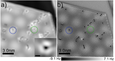
We start by characterizing the structure of the islands after Ne bombardment. The STM images (Fig. 1a) reveal the typical hexagonal structure originating in the moiré superstructure forming as a consequence of the lattice mismatch between the terminating S layer and the Au(111) substrate. At the same time, the image also reveals randomly distributed features, consisting of a dark center and a bright rim. A close-up view on one of these defects is displayed in the inset of Fig. 1a. The rim appears with a three-fold symmetric shape. A similar shape has been reported from theoretical and experimental studies of chalcogen vacancies in (other) TMDCs [32, 33, 34, 20]. It is thus tempting to assign these defects to missing S atoms. Yet, to obtain complementary insights into the origin of the defects, we probed the frequency-shift () signal of the very same area (Fig. 1b). This image resolves the atomic structure of the top S layer, and confirms that some S atoms are missing. Comparison of the STM and AFM image allows us to associate most of the dark features surrounded by a bright rim to S vacancies. One of these is highlighted with the blue circle in Fig. 1a,b. When several S atoms are missing in neighboring sites, the rim shape is distorted. However, some few bright features in the STM image can not be assigned to missing top-layer S atoms as the top layer remains intact (green circles in Fig. 1a,b). Hence, these must originate in interstitials or bottom-layer sulfur vacancies [32] that have been incorporated in the layer during its growth process.
IV Electronic and magnetic properties of sulfur vacancies
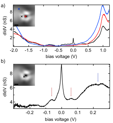
Having successfully created top-layer S vacancies, we now turn to their electronic characterization. For comparison, we first present a d/d spectrum on the intact . It shows the semiconducting band gap, flanked by the onset of the valence band at -1.6 V and the onset of the conduction band at 0.9 V [Fig. 2a (blue)] [31]. A d/d spectrum recorded in the center of the S vacancy (red) looks very similar to the bare spectrum, yet, with the onset and the peak of the conduction band being shifted by a few tens of mV. The most notable feature associated to the S vacancy is, however, found on the three-fold symmetric rim. Here, we detect a peak at the Fermi level, which is better brought out in the close-up view in Fig. 2b. Additionally, we observe two narrow resonances at 60 mV and a broad one at 230 mV.
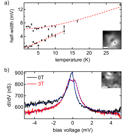
To unravel the origin of the zero-bias peak, we investigated the evolution of d/d spectra of several S vacancies with increasing temperature. We fit all lineshapes by a Frota function (for an example see Fig.3b) and extract their half-widths after subtraction of the Fermi-Dirac temperature broadening [35, 36]. The results are plotted in Fig. 3a for two distinct defects. Both peak broadenings can be reproduced by the phenomenological expression for the temperature dependence of a spin-1/2 Kondo resonance [38, 39, 40]:
| (1) |
albeit with different Kondo temperatures of K and K, respectively. The temperature dependencies thus indicate the presence of single-electron spins around the defect sites, which are exchange coupled to the substrate. We comment on the origin of the different Kondo temperatures below.
To further support the interpretation of the zero-bias peak as a Kondo resonance, we probe its behavior in an external magnetic field of 3 T perpendicular to the sample. Figure 3b shows such a d/d spectrum recorded on a S vacancy with a low Kondo temperature. The splitting of the resonance is in agreement with a Zeeman split of a spin-1/2 resonance and a -factor of 2 (Fig. 3b). (Zero-bias peaks with significantly larger width, and thus larger Kondo temperatures, cannot be split in a magnetic field up to 3 T.) Following the assignment of the zero-bias peak as a Kondo resonance, the two narrow resonances at 60 mV in the d/d spectra (Fig. 2b) can tentatively be assigned to excitation of the singly-occupied resonance at negative bias voltage, separated by the Coulomb charging energy mV to the doubly occupied state at positive bias voltage [37, 41].
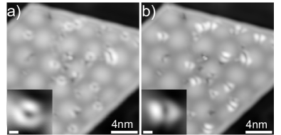
As already mentioned above, we find different Kondo temperatures for different S vacancies. The extracted Kondo temperatures vary in a range from 4-220 K. We ascribe such large variation to the different sites of the defects with respect to the moiré structure of the layer. A similar observation was made for Fe and Mn atoms and was explained by the modulated density of states at the Fermi level by the moiré structure [42, 43]. Another indication of the moiré structure influencing the Kondo effect is found in the spatial distribution of the Kondo amplitude. While the electronic structure imaged at larger bias voltage revealed a three-fold symmetric rim (Fig. 1a and 4a), the Kondo amplitude of most vacancies shows an almost two-fold symmetric shape (Fig. 4b and inset). These distributions reflect the local symmetry of the moiré structure with the mirror axis aligning along the valleys of the moiré modulation. Hence, all our observations point to a strong impact of the electronic modulation of the density of states on the Kondo effect. However, we cannot exclude that some of the S defects may be occupied by rest-gas molecules from the UHV chamber, such as oxygen, which are hard to be distinguished from the bare S vacancies [44, 45].
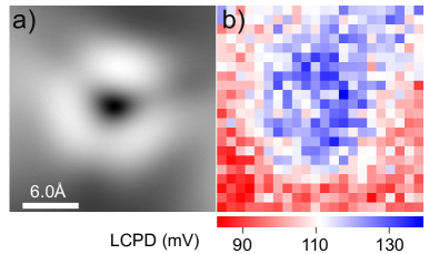
An unpaired electron spin must originate in a localized charge. To investigate the local charge distribution we measure the local-contact-potential difference (LCPD) using a tuning-fork AFM. We extract the LCPD values from a grid of spectra (Fig. 5b). Comparing to the simultaneously recorded STM image, we associate the increase in LCPD to the S-vacancy site. A more positive LCPD value implies a negative charge localization, suggesting electron transfer from the metal to the defect site. This charge transfer is consistent with density-functional-theory calculations of S vacancies in on Au(111) [23]. Concomitant to the charge transfer, theory also predicts a Jahn-Teller distortion of the atomic structure [21, 23]. However, the expected atomic displacements are very small ( Å) and not unambiguously detectable in our AFM images.
V Sulfur vacancies in patches of quasi-free-standing
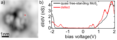
We have thus established that the Au substrate is of crucial importance for the formation of singly-charged S vacancies, which are Kondo screened. To obtain direct insight into the role of the metal, it would be illuminating to investigate the same vacancies in the absence of the metal substrate. To do so, we take advantage of another type of defect of the /Au(111) sample. Some areas of the islands, typically of several nanometers in diameter, appear slightly darker at large bias voltages and completely transparent at low bias voltage. These areal defects have been ascribed to the absence of a single atomic layer of Au atoms below the [46]. Figure 6a shows such an area (dark background) decorated by three S vacancies. Differential conductance spectra on such an area without S vacancies exhibit a band gap of similar width as expected for an isolated monolayer [47]. The conductance in the gap is almost zero and the onsets of the valence and conduction band are much sharper than on Au (Fig. 6b). Hence, hybridization with the metal is negligible and we thus refer to these areas as quasi free-standing monolayers [46]. Spectra taken on the S-vacancy sites show a resonance at -1.4 V in the occupied states and two unoccupied states at 450 mV and 650 mV within this band gap, whereas the region close to the Fermi level is essentially flat. A state close to the valence-band edge along with a spin-orbit split state in the unoccupied regime of the band gap have been predicted for free-standing and to arise from dangling bonds with strong Mo- character [32, 21, 48, 23]. Our observations are thus in agreement with a neutral vacancy state, which is stable in the absence of hybridization with a metal support, as e.g. also observed in WS2 on silicon carbide [34].
VI Conclusions
The characterization of defects in monolayers of TMDCs is of crucial importance for understanding the performance of electronic devices made of TMDC heterostructures. Here, we deliberately created S vacancies in monolayers of grown on a Au(111) surface by Ne-ion bombardment. We showed that these defects are singly charged, which we ascribe to charge transfer from the metal substrate. The localized electron is Kondo screened by the electron bath at the interface of to Au(111). Owing to a moiré-induced modulation of the density of states at the Fermi level, the exchange coupling to the substrate varies depending on the specific location of the S vacancy. Removal of a single Au layer in a small area below the immediately suppresses charge transfer. Our results highlight the impact of a metal substrate for controlling the charge state and magnetic properties of single-atom defects in .
Acknowledgements.
We thank Blanca Biel, Laëtitia Farinacci, Mariana Rossi and Rika Simon for fruitful discussions. We acknowledge financial support by the Deutsche Forschungsgemeinschaft (DFG, German Research Foundation) through project number 328545488 (TRR 227, project B05).References
- Wang et al. [2012] Q. H. Wang, K. Kalantar-zadeh, A. Kis, J. Coleman, and M. Strano, Electronics and Optoelectronics of Two-Dimensional Transition Metal Dichalcogenides, Nature Nanotech. 7, 699 (2012).
- Novoselov et al. [2016] K. S. Novoselov, A. Mishchenko, A. Carvalho, and A. H. C. Neto, 2D materials and van der Waals heterostructures, Science 353, aac9439 (2016).
- Hu et al. [2018] Z. Hu, Z. Wu, C. Han, J. He, Z. Ni, and W. Chen, Two-dimensional transition metal dichalcogenides: interface and defect engineering, Chem. Soc. Rev. 47, 3100 (2018).
- Liang et al. [2021] Q. Liang, Q. Zhang, X. Zhao, M. Liu, and A. T. S. Wee, Defect engineering of two-dimensional transition-metal dichalcogenides: Applications, challenges, and opportunities, ACS Nano 15, 2165 (2021).
- Qiu et al. [2013a] H. Qiu, T. Xu, Z. Wang, W. Ren, H. Nan, Z. Ni, Q. Chen, S. Yuan, F. Miao, F. Song, G. Long, Y. Shi, L. Sun, J. Wang, and X. Wang, Hopping transport through defect-induced localized states in molybdenum disulphide, Nature Commun. 4 (2013a).
- Yu et al. [2014] Z. Yu, Y. Pan, Y. Shen, Z. Wang, Z.-Y. Ong, T. Xu, R. Xin, L. Pan, B. Wang, L. Sun, J. Wang, G. Zhang, Y. W. Zhang, Y. Shi, and X. Wang, Towards intrinsic charge transport in monolayer molybdenum disulfide by defect and interface engineering, Nature Commun. 5, 5290 (2014).
- KC et al. [2014] S. KC, R. C. Longo, R. Addou, R. M. Wallace, and K. Cho, Impact of intrinsic atomic defects on the electronic structure of MoS2 monolayers, Nanotechnology 25, 375703 (2014).
- Nan et al. [2014] H. Nan, Z. Wang, W. Wang, Z. Liang, Y. Lu, Q. Chen, D. He, P. Tan, F. Miao, X. Wang, J. Wang, and Z. Ni, Strong photoluminescence enhancement of MoS2 through defect engineering and oxygen bonding, ACS Nano 8, 5738 (2014).
- Chow et al. [2015] P. K. Chow, R. B. Jacobs-Gedrim, J. Gao, T.-M. Lu, B. Yu, H. Terrones, and N. Koratkar, Defect-induced photoluminescence in monolayer semiconducting transition metal dichalcogenides, ACS Nano 9, 1520 (2015).
- Lin et al. [2018] Y.-C. Lin, S. Li, H.-P. Komsa, L.-J. Chang, A. V. Krasheninnikov, G. Eda, and K. Suenaga, Revealing the atomic defects of governing its distinct optical emissions, Adv. Funct. Mat. 28, 1704210 (2018).
- Chee et al. [2020] S.-S. Chee, W.-J. Lee, Y.-R. Jo, M. K. Cho, D. Chun, H. Baik, B.-J. Kim, M.-H. Yoon, K. Lee, and M.-H. Ham, Atomic vacancy control and elemental substitution in a monolayer molybdenum disulfide for high performance optoelectronic device arrays, Adv. Funct. Mat. 30, 1908147 (2020).
- Yang et al. [2020] J. Yang, F. Bussolotti, H. Kawai, and K. E. J. Goh, Tuning the conductivity type in monolayer and MoS2 by sulfur vacancies, phys. stat. sol. (RRL) 14, 2000248 (2020).
- Bussolotti et al. [2021] F. Bussolotti, J. Yang, H. Kawai, C. P. Y. Wong, and K. E. J. Goh, Impact of S-Vacancies on the Charge Injection Barrier at the Electrical Contact with the MoS2 Monolayer, ACS Nano 15, 2686 (2021), pMID: 33502172.
- Mitterreiter et al. [2021] E. Mitterreiter, B. Schuler, A. Micevic, D. Hernangomez-Perez, K. Barthelmi, K. A. Cochrane, J. Kiemle, F. Sigger, J. Klein, E. Wong, E. S. Barnard, K. Watanabe, T. Taniguchi, M. Lorke, F. Jahnke, J. J. Finley, A. M. Schwartzberg, D. Y. Qiu, S. Refaely-Abramson, A. W. Holleitner, A. Weber-Bargioni, and C. Kastl, The role of chalcogen vacancies for atomic defect emission in MoS2, Nat. Commun. 12, 3822 (2021).
- Lin et al. [2022] Y. Lin, E. Hathaway, F. Habis, Y. Wang, R. G. Rodriguez, K. Alnasser, N. Hurley, and J. Cui, Enhanced emission from defect levels in multilayer MoS2, Adv. Opt. Mat. 10, 2201059 (2022).
- Li et al. [2016] H. Li, C. Tsai, A. L. Koh, L. Cai, A. W. Contryman, A. H. Fragapane, J. Zhao, H. S. Han, H. C. Manoharan, F. Abild-Pedersen, J. K. Nørskov, and X. Zheng, Activating and optimizing MoS2 basal planes for hydrogen evolution through the formation of strained sulphur vacancies, Nature Mater. 15, 48 (2016).
- Zhou et al. [2013] W. Zhou, X. Zou, S. Najmaei, Z. Liu, Y. Shi, J. Kong, J. Lou, P. M. Ajayan, B. I. Yakobson, and J.-C. Idrobo, Intrinsic structural defects in monolayer molybdenum disulfide, Nano Lett. 13, 2615 (2013).
- Komsa and Krasheninnikov [2015] H.-P. Komsa and A. V. Krasheninnikov, Native defects in bulk and monolayer MoS2 from first principles, Phys. Rev. B 91, 125304 (2015).
- Lin et al. [2016] Z. Lin, B. R. Carvalho, E. Kahn, R. Lv, R. Rao, H. Terrones, M. A. Pimenta, and M. Terrones, Defect engineering of two-dimensional transition metal dichalcogenides, 2D Materials 3, 022002 (2016).
- Tumino et al. [2020] F. Tumino, C. S. Casari, A. Li Bassi, and S. Tosoni, Nature of point defects in single-layer MoS2 supported on Au(111), J. Phys. Chem. C 124, 12424 (2020).
- Tan et al. [2020] A. M. Z. Tan, C. Freysoldt, and R. G. Hennig, Stability of charged sulfur vacancies in 2d and bulk MoS2 from plane-wave density functional theory with electrostatic corrections, Phys. Rev. Mater. 4, 064004 (2020).
- Yang et al. [2019] J. Yang, H. Kawai, C. P. Y. Wong, and K. E. J. Goh, Electrical Doping Effect of Vacancies on Monolayer MoS2, J. Phys. Chem. C 123, 2933 (2019).
- [23] A. Akkoush, Y. Litman, and M. Rossi, A Hybrid-Density Functional Theory Study of Intrinsic Point Defects in MX2 (M=Mo,W; X=S,Se) Monolayers, phys. stat. sol. (a) , 2300180.
- Li et al. [2018] A. Li, J. Pan, Z. Yang, L. Zhou, X. Xiong, and F. Ouyang, Charge and strain induced magnetism in monolayer MoS2 with S vacancy, J. Magn. Magn. Mater. 451, 520 (2018).
- Tongay et al. [2012] S. Tongay, S. S. Varnoosfaderani, B. R. Appleton, J. Wu, and A. F. Hebard, Magnetic properties of MoS2: Existence of ferromagnetism, Appl. Phys. Lett. 101, 123105 (2012).
- Jolie et al. [2019] W. Jolie, C. Murray, P. S. Weiß, J. Hall, F. Portner, N. Atodiresei, A. V. Krasheninnikov, C. Busse, H.-P. Komsa, A. Rosch, and T. Michely, Tomonaga-Luttinger Liquid in a Box: Electrons Confined within Mirror-Twin Boundaries, Phys. Rev. X 9, 011055 (2019).
- van Efferen et al. [2023] C. van Efferen, J. Fischer, T. A. Costi, A. Rosch, T. Michely, and W. Jolie, Modulated Kondo screening along magnetic mirror twin boundaries in monolayer MoS2 on graphene (2023), arXiv:2210.09675 [cond-mat.mes-hall] .
- Splendiani et al. [2010] A. Splendiani, L. Sun, Y. Zhang, T. Li, J. Kim, C. Chim, G. Galli, and F. Wang, Emerging photoluminescence in monolayer MoS2, Nano Lett. 10, 1271 (2010).
- Mak et al. [2010] K. F. Mak, C. Lee, J. Hone, J. Shan, and T. F. Heinz, Atomically thin MoS2: A new direct-gap semiconductor, Phys. Rev. Lett. 105, 136805 (2010).
- Bruix et al. [2016] A. Bruix, J. A. Miwa, N. Hauptmann, D. Wegner, S. Ulstrup, S. S. Grønborg, C. E. Sanders, M. Dendzik, A. Grubiić abo, M. Bianchi, J. V. Lauritsen, A. A. Khajetoorians, B. Hammer, and P. Hofmann, Single-layer on Au(111): Band gap renormalization and substrate interaction, Phys. Rev. B 93, 165422 (2016).
- Krane et al. [2018] N. Krane, C. Lotze, and K. J. Franke, Moiré structure of MoS2 on Au(111): Local structural and electronic properties, Surf. Sci. 678, 136 (2018).
- Gonzalez et al. [2016] C. Gonzalez, B. Biel, and Y. J. Dappe, Theoretical characterisation of point defects on a MoS2 monolayer by scanning tunnelling microscopy, Nanotechnology 27, 105702 (2016).
- Vancso et al. [2016] P. Vancso, G. Z. Magda, J. Petö, J.-Y. Noh, Y.-S. Kim, C. Hwang, L. P. Biro, and L. Tapaszto, The intrinsic defect structure of exfoliated single layers revealed by Scanning Tunneling Microscopy, Sci. Rep. 6, 29726 (2016).
- Schuler et al. [2019] B. Schuler, D. Y. Qiu, S. Refaely-Abramson, C. Kastl, C. T. Chen, S. Barja, R. J. Koch, D. F. Ogletree, S. Aloni, A. M. Schwartzberg, J. B. Neaton, S. G. Louie, and A. Weber-Bargioni, Large spin-orbit splitting of deep in-gap defect states of engineered sulfur vacancies in monolayer , Phys. Rev. Lett. 123, 076801 (2019).
- Prüser et al. [2011] H. Prüser, M. Wenderoth, P. E. Dargel, A. Weismann, R. Peters, T. Pruschke, and R. G. Ulbrich, Long-range Kondo signature of a single magnetic impurity, Nature Phys. 7, 203 (2011).
- Frank and Jacob [2015] S. Frank and D. Jacob, Orbital signatures of Fano-Kondo line shapes in STM adatom spectroscopy, Phys. Rev. B 92, 235127 (2015).
- Goldhaber-Gordon et al. [1998] D. Goldhaber-Gordon, J. Göres, M. A. Kastner, H. Shtrikman, D. Mahalu, and U. Meirav, From the Kondo Regime to the Mixed-Valence Regime in a Single-Electron Transistor, Phys. Rev. Lett. 81, 5225 (1998).
- Nozieres [1974] P. Nozieres, A fermi-liquid description of the Kondo problem at low temperatures, J. Low Temp. Phys. 17, 31 (1974).
- Madhavan et al. [1998] V. Madhavan, W. Chen, T. Jamneala, M. F. Crommie, and N. S. Wingreen, Tunneling into a single magnetic atom: Spectroscopic evidence of the kondo resonance, Science 280, 567 (1998).
- Nagaoka et al. [2002] K. Nagaoka, T. Jamneala, M. Grobis, and M. F. Crommie, Temperature dependence of a single kondo impurity, Phys. Rev. Lett. 88, 077205 (2002).
- Fernández-Torrente et al. [2008] I. Fernández-Torrente, K. J. Franke, and J. I. Pascual, Vibrational Kondo effect in pure organic charge-transfer assemblies, Phys. Rev. Lett. 101, 217203 (2008).
- Trishin et al. [2021] S. Trishin, C. Lotze, N. Bogdanoff, F. von Oppen, and K. J. Franke, Moiré Tuning of Spin Excitations: Individual Fe Atoms on , Phys. Rev. Lett. 127, 236801 (2021).
- Trishin et al. [2023] S. Trishin, C. Lotze, F. Lohss, G. Franceschi, L. I. Glazman, F. von Oppen, and K. J. Franke, Tuning a Two-Impurity Kondo System by a Moiré Superstructure, Phys. Rev. Lett. 130, 176201 (2023).
- Barja et al. [2019] S. Barja, S. Refaely-Abramson, B. Schuler, D. Y. Qiu, A. Pulkin, S. Wickenburg, H. Ryu, M. M. Ugeda, C. Kastl, C. Chen, C. Hwang, A. Schwartzberg, S. Aloni, S.-K. Mo, D. Frank Ogletree, M. F. Crommie, O. V. Yazyev, S. G. Louie, J. B. Neaton, and A. Weber-Bargioni, Identifying substitutional oxygen as a prolific point defect in monolayer transition metal dichalcogenides, Nat. Commun. 10, 3382 (2019).
- Cochrane et al. [2021] K. A. Cochrane, J.-H. Lee, C. Kastl, J. B. Haber, T. Zhang, A. Kozhakhmetov, J. A. Robinson, M. Terrones, J. Repp, J. B. Neaton, A. Weber-Bargioni, and B. Schuler, Spin-dependent vibronic response of a carbon radical ion in two-dimensional , Nat. Commun. 12, 7287 (2021).
- Krane et al. [2016] N. Krane, C. Lotze, J. M. Läger, G. Reecht, and K. J. Franke, Electronic structure and luminescence of quasi-freestanding MoS2 nanopatches on Au(111), Nano Lett. 16, 5163 (2016).
- Qiu et al. [2013b] D. Y. Qiu, F. H. da Jornada, and S. G. Louie, Optical spectrum of MoS2: Many-body effects and diversity of exciton states, Phys. Rev. Lett. 111, 216805 (2013b).
- Sorkin et al. [2022] V. Sorkin, H. Zhou, Z. G. Yu, K.-W. Ang, and Y.-W. Zhang, The effects of point defect type, location, and density on the Schottky barrier height of Au/ heterojunction: a first-principles study, Sci. Rep. 12, 18001 (2022).