Perpendicular electronic transport and moiré-induced resonance in twisted interfaces of three-dimensional graphite
Abstract
We calculate the perpendicular electrical conductivity in twisted three-dimensional graphite (rotationally stacked graphite pieces) by using the effective continuum model and the recursive Green’s function method. In the low twist angle regime , the conductivity shows a nonmonotonic dependence with a peak and dip structure as a function of the twist angle. By analyzing the momentum-resolved conductance and the local density of states, this behavior is attributed to the Fano resonance between continuum states of bulk graphite and interface-localized states, which is a remnant of the flat band in the magic-angle twisted bilayer graphene. We also apply the formulation to the high-angle regime near the commensurate angle , and reproduce the conductance peak observed in the experiment.
I Introduction
In recent years, the field of twisted two-dimensional (2D) materials has attracted attention due to their unique and tunable physical properties. The concept of twisting 2D materials involves stacking two or more layers of the same or different materials with a specific twist angle between them. A representative system is twisted bilayer graphene (TBG), which consists of two graphene layers being rotated with respect to each other. TBG hosts extremely flat bands at the Fermi energy at the so-called magic angle [1], where various correlated phenomena have been experimentally observed [2; 3]. Beyond TBG, the scope of research in the field has expanded to encompass twisted multilayers, including twisted trilayer graphene [4; 5; 6; 7; 8; 9; 10; 11], twisted double bilayer graphene (twist stack of two pieces of a Bernal-stacked bilayer) [12; 13; 14; 15; 16; 17; 18; 19; 20] and twisted monolayer-bilayer graphene (monolayer and Bernal-stacked bilayer) [21; 22; 23; 24; 25; 26]. In addition, research on twisted multilayer graphenes composed of a more general number of layers and configurations has also been conducted [27; 28; 29; 30; 31; 32; 33; 34; 35; 36; 37]. These systems often exhibit flat bands and associated peculiar physical properties.
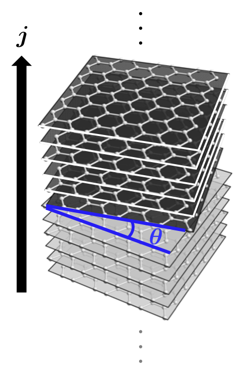
This paper aims to extend the exploration to twisted three-dimensional (3D) systems where 3D layered materials are rotationally stacked as shown in Fig. 1. In particular, we focus on the twist-angle-dependent transport in the out-of-plane (perpendicular) direction, to explore measurable properties associated with the moiré pattern. The conduction across twisted interfaces has been studied for various tunneling junctions with an insulating barrier in the middle, such as the graphene/hexagonal boron nitride/graphene structure [38; 39; 40; 41; 42; 43; 44]. In these systems, the transport through the junction can be captured by a conventional perturbation approach including the tunneling process in the leading order [40; 41; 45].
When two materials are directly contacted, however, the multiple scattering at the twisted interface is generally relevant. Here we consider a twisted 3D graphite (Fig. 1) as the simplest example of directly contacted twisted 3D systems. The electronic structure of the twisted 3D graphite was previously studied, where a remnant of the flat band in TBG was found in the local density of states [29]. The interlayer transport in twisted graphitic systems was investigated in various theoretical approaches [46; 47; 48; 49; 50], and it was also experimentally probed in angle-variable devices [51; 52; 53; 54; 55; 56; 57]. In large twist angles (), it was predicted that the perpendicular conductance is enhanced near the commensurate angles where the atomic structure becomes exactly periodic [46], and it was actually observed in conductance measurements as a sharp conductance peak against the twist angle [54; 51; 53]. In this regime, the tunneling probability is small and the leading-order approximation in the transport is still valid.
In the present paper, we focus on the low twist angle regime where the multiple-scattering event is dominant. We find a special resonant behavior in the electronic transport due to the interface-localized states, which corresponds to the moiré flat band in TBG. Specifically, we calculate the perpendicular electrical conductivity in twisted 3D graphite by combining the effective continuum model and the recursive Green’s function method [58; 59; 60], to properly treat higher-order terms in the transmission. In the low twist angle regime , in particular, we find that the perpendicular conductivity exhibits a peak-and-dip structure as a function of the twist angle. By analyzing the momentum-resolved conductance and the local density of states, we attribute the sharp rise and drop of the conductivity to a Fano resonance between bulk states and the interface-localized states. For the graphite band model, we adopt a simplified circularly symmetric model as well as a more realistic version with the Slonczewski-Weiss-McClure (SWM) parameters fully included [61; 62]. We confirm that the qualitative result does not depend on the choice of the models. In the latter part of the paper, we apply the formulation to the high-angle regime near the commensurate angle , and simulate the conductance peak observed in the experiment [54; 51; 53]. The formulation is applicable to general twisted 3D systems, such as a twisted interface of which exhibits the Josephson effect in the superconducting state [63].
This paper is organized as follows. In Sec. II, we introduce an effective continuum Hamiltonian of twisted graphite. In Sec. III, we formulate the procedure to calculate the perpendicular electrical conductivity in twisted 3D systems using the recursive Green’s function method and the effective continuum model. In Sec. IV, we calculate the conductivity for 3D graphite with various twist angles, and find the non-monotonic behavior of the perpendicular conductivity. In Sec. V, we discuss the origin of the twist angle-dependence of the perpendicular conductivity. We examine the momentum-resolved conductance and show that its sudden drop is due to the Fano resonance caused by the interface-localized state. In Sec. VI, we discuss the perpendicular conductivity near the second commensurate angle . Finally, the conclusion is given in Sec. VII.
II Hamiltonian of twisted graphite
II.1 Band models for bulk graphite
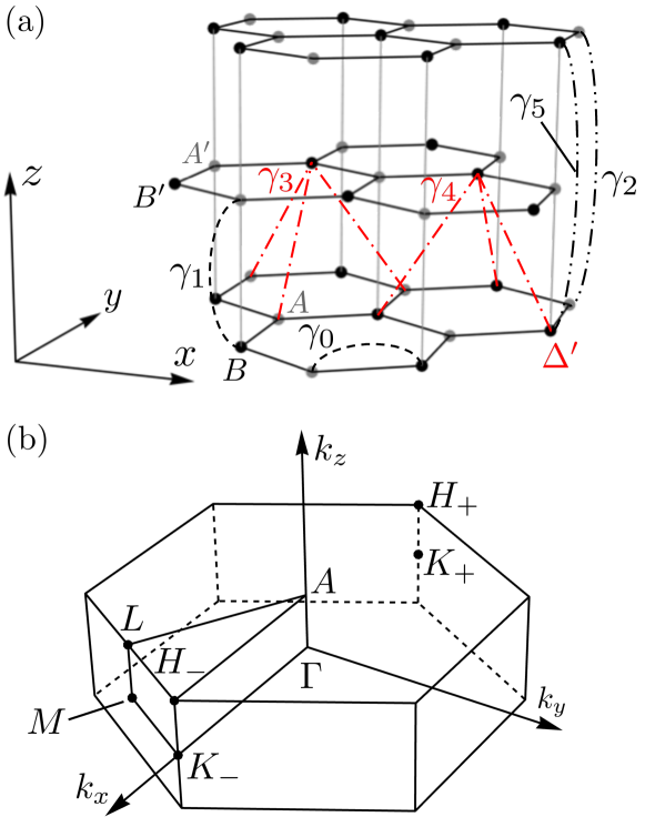
The crystal structure of Bernal-stacking (AB-stacking) graphite is shown in Fig. 2(a). A unit cell contains four atomic sites , where and are arranged along vertical columns while and are located above or below the center of hexagons in the neighboring layers. The lattice constants are given by nm and nm for the in-plane and perpendicular direction, respectively. We define primitive lattice vectors by , and . The Brillouin zone is a hexagonal prism spanned by the reciprocal lattice vectors , , and , as shown in Fig. 2(b). The Fermi surfaces are located around , which are referred to as and points, respectively.
We describe the electronic bands of graphite using the SWM model [61; 62; 64; 65]. The model contains six hopping parameters and an onsite energy , which are visualized in Fig. 2(a). We use the values tabulated in Table 1.
Taking the Bloch states as the basis, the SWM Hamiltonian around the point is given by
| (1) |
where is the in-plane wavenumber measured from the point, , , and . In this paper, we consider a simple model where we neglect , and , and the full-parameter model which contains all of the parameters.
The band structures and Fermi surfaces for these two models are shown in Fig. 3. Due to the parameter, the band structure obtains the dispersion along , which gives rise to the formation of the electron and hole pocket.
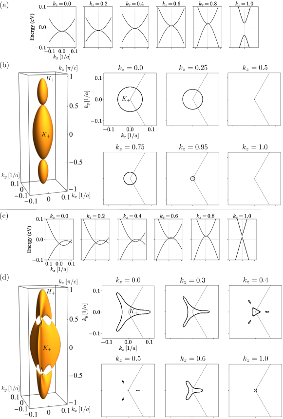
Notably, the isotropic Fermi surface in the simple model is warped in a 120∘-symmetric manner in the full-parameter model. This trigonal warping effect is due to the entry of the parameter.
II.2 Twisted graphite
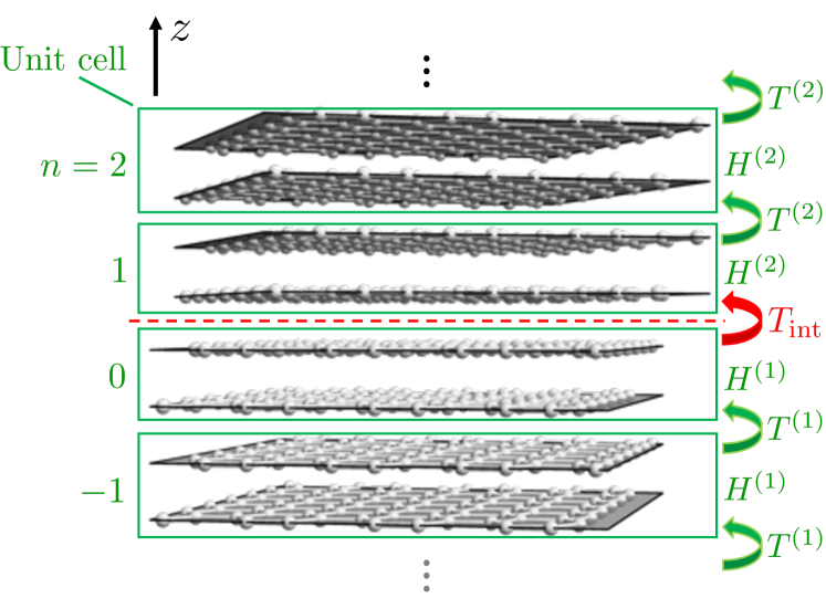
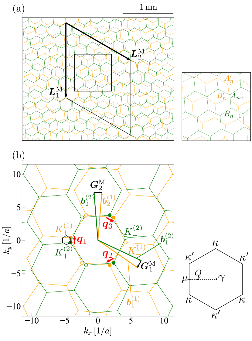
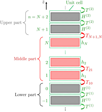
We define a twisted graphite as a pair of half-infinite pieces of Bernal-stacking graphite contacted with a certain twist angle . A schematic illustration is given in Fig. 4, where we label unit cells of graphite (extending over two graphene layers) by . Here and correspond to upper and lower graphite pieces, respectively, and we label sublattices in the th cell as .
At the interface, a long-scale moiré pattern is formed. Figure 5(a) illustrates the atomic structure of the twisted interface between the th and th cells. We define the primitive lattice vectors of the lower () and upper () graphite as , and also the primitive reciprocal vectors as , where
| (2) |
and is the rotation matrix by an angle . Accordingly, the corner points of the Brillouin zones are given by .
The moiré Brillouin zone (MBZ) is defined by the reciprocal vectors , as depicted in Fig. 5(b). We also introduce the displacement of the point as , and also for the other two equivalent corners. We have relationships and . The primitive moiré lattice vector in the real space is determined by [see Fig. 5(a)], giving for [66].
We describe the electronic structure of twisted graphite by an effective continuum model similar to twisted bilayer graphene [1; 67]. In a basis of , the Hamiltonian of twisted graphite can be written as
| (3) |
where and are blocks with and 2 indicating the lower and upper graphite sectors, respectively, which are given by
| (4) |
Here and are defined in Eq. (1).
is the interlayer Hamiltonian matrix for the twisted interface, which is given by [1; 67]
| (5) |
where , , and [67]. By starting from a lower-graphite Bloch state of the wavenumber , the interlayer Hamiltonian hybridizes a set of wavenumbers of the same valley,
| (6) |
of the upper and lower parts, respectively (: integers). To write down the Hamiltonian as a finite-sized matrix, we consider a finite set of wavenumbers inside a certain cutoff circle . Note that is a parameter which moves inside a moiré Brillouin zone spanned by and [Fig. 5(b)]. In this representation, , and in Eq. (3) are matrices, where is the number of different wavenumbers in the set of , and the factor 4 is for the sublattices (). The matrices and are diagonal in the label , while only the matrix hybridizes different ’s.
III Electrical conductivity in general twisted interface
In this section, we formulate a method to calculate the perpendicular electrical conductivity and the local density of states (LDOS) in general twisted 3D systems. We consider a layered system as shown in Fig. 6, which consists of slices labeled by indices . A slice can be a single atomic layer or a cluster of layers. The whole system is composed of the lower (), middle (), and upper () parts. We assume that the lower and upper parts are periodic in the direction (perpendicular to the layer) with a single period corresponding to a single . The middle part can be periodic or nonperiodic in the direction, and they can be arranged in a general orientation. We require that all the layers in the upper, middle and lower parts share a common super-periodicity in in-plane directions (e.g., the moiré period for the twisted graphite), so that the Hamiltonian becomes a finite matrix in a momentum representation, under a certain -space cutoff. The twisted graphite corresponds to a system without a middle part , while we can formally assign the middle part within the same system by taking an arbitrary number of upper and lower layers including the twisted interface. We apply the formulation with to the calculation of the conductivity, while a formalism with a finite middle part can be used to calculate the LDOS near the interface, where the middle part is set to contain the desired region.
In a similar manner to the twisted graphite in the previous section, the Hamiltonian of the system is written as
| (7) |
where represents the Hamiltonian of a single slice in the lower () and upper () regions, and is the hopping matrix between neighboring slices. and are matrices. Here, we ignore hopping terms across more than two slices. This is justified by taking sufficiently large slices. and are intra- and interslice matrices, respectively, in the middle part. The dimension of is arbitrary. The total Hamiltonian is labeled by in the Brillouin zone corresponding to the in-plane supercell of the system.
The electrical conductance in the perpendicular direction can be calculated by applying the recursive Green’s function method [60; 68] to the Hamiltonian Eq. (20). Specifically, we calculate eigenchannels of the upper and lower periodic parts, and express transmission coefficients between these channels using the Green’s function, as follows.
To obtain the eigenchannels, we solve the Schrödinger equation for the upper and lower periodic parts
| (8) |
where is the eigenenergy and is -component vector. We first assume a solution of Bloch’s form . By using , we obtain
| (9) |
Equation (9) can be viewed as a eigenvalue problem with an eigenvalue . For a given energy , we obtain upward-going solutions with eigenvalues , and downward-going solutions with . Here upward- (downward-) going solutions include propagating modes in the positive (negative) direction and evanescent modes decaying in the positive (negative) direction.
A general solution at can be written in a linear combination of these eigenfunctions as
| (10) |
The wavefunction at general positions can be found by
| (11) |
where
| (12) |
are matrices.
An eigenvalue equation for the middle part is then written as [60]
| (13) | |||
| (20) |
where () represents the self energy matrix for the open leads in the lower (upper) part, which are defined by
| (21) |
The term with on the right-hand side of Eq. (13) represents a source term associated with the incident wave from the lower channels. The Green’s function of the system is defined by . To obtain this, the recursive method can be utilized. The details of the method are explained in Appendix A.
Once we have the Green’s function , the transmission coefficients are obtained by
| (22) |
where is the group velocity of the -th upward eigenmodes in the lower (upper) bulk. The matrix is the partial block of the Green’s function:
| (23) |
From the Landauer formula [69], the electrical conductance in the out-of-plane direction is obtained by
| (24) |
where the factor is for the spin degree of freedom. Finally, the total conductivity across the interface per unit area is obtained by
| (25) |
where is the total cross section of the system along the - plane. The contact resistivity of the twisted interface is given by .
We can also calculate LDOS in the middle part from the Green’s function. The LDOS of the -th slice is obtained as
| (26) |
where the trace sums up sublattice or orbital degrees freedom and also the in-plane wavenumbers to span the Hamiltonian matrix. In twisted graphite, a slice is composed of two graphene monolayers. To calculate the LDOS of each layer, we can restrict the summation over sublattices in the trace in Eq.(26) to just or .
IV Electrical conductivity in twisted graphite interface
We calculate the perpendicular electrical conductivity of twisted graphite by applying Eq. (25) to the Hamiltonian Eq. (3), with no middle part. Figure 7 shows the conductivity as a function of the twist angle , calculated for (a) the simple graphite model and (b) the full parameter model (see Sec. II.1). Here we take the Fermi energy at the charge neutral point, . The vertical axis is scaled by on the left, and also by on the right. The represents the ballistic conductance of bulk 3D graphite, and can be regarded as an effective transmission coefficient.
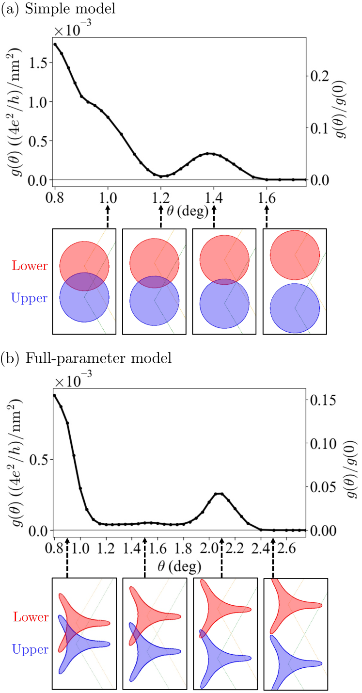
In the simple model [Fig. 7(a)], the conductivity decreases when the twist angle is increased, and it completely vanishes in . This tendency can be understood in terms of the overlap of the Fermi surfaces. By a twist, the Brillouin zones of the upper and lower graphite are rotated by [see Fig. 5(b)], and then the in-plane projections of respective Fermi surfaces are separated as shown by blue and red filled circles in Fig. 7(a). Obviously, the overlapped region of the Fermi surface projections is diminished with increase of the angle, and the conductivity drops accordingly. For , the two Fermi surfaces are completely separated and the conductivity goes to zero. Notably, we observe a non-monotonic behavior in the range of , where the conductivity reaches nearly zero at , and it takes a peak at . This cannot be simply explained by the Fermi surface overlap, which just monotonically decreases in increasing the twist angle.
We also see a similar behavior in the full-parameter model as well, as shown in Fig. 7(b). With the increase of the twist angle, the conductance drops down to , while it recovers and peaks at . It finally vanishes in where the Fermi surface overlap disappears.
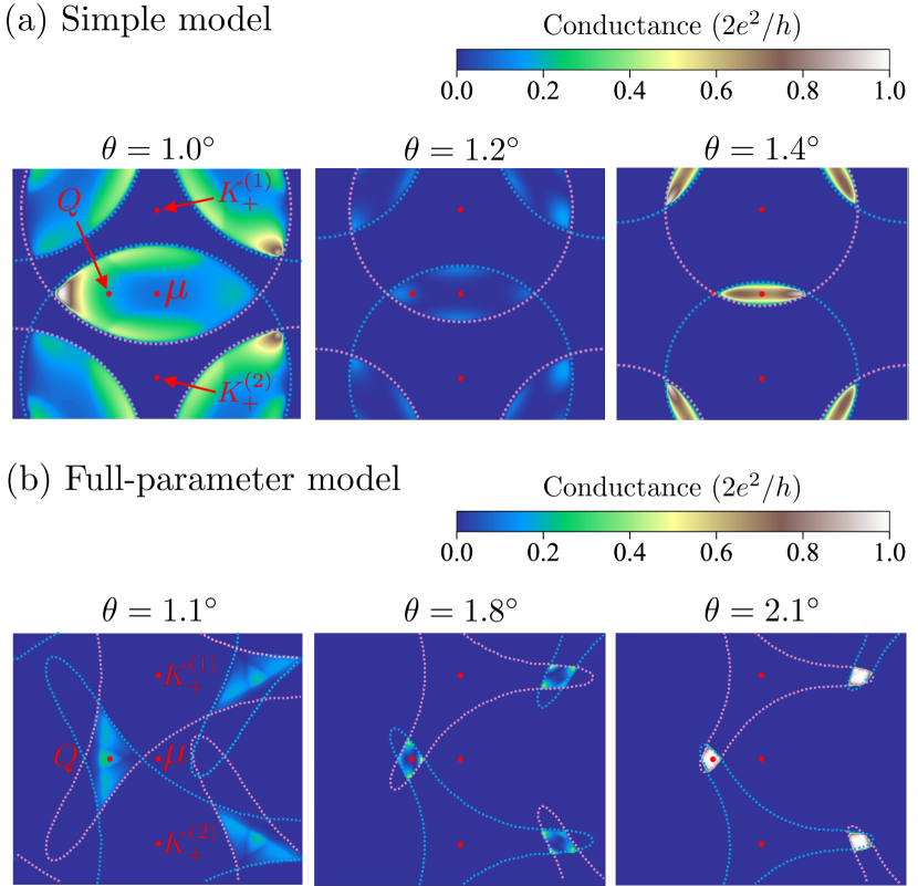
To consider the origin of the dip-and-peak structure, we examine the -resolved conductance defined by Eq. (24). Figure 8(a) shows the density plot of on -space, calculated for the simple model. The red (blue) circle represents the outline of the upper (lower) projected Fermi surface. We observe that the finite amplitude is indeed present only in the overlapping region. At , however, the -resolved conductance is strongly suppressed around the overlap center at the point, and actually this vanishing amplitude is responsible for the dip of total conductivity at [Fig. 7(a)]. In the full-parameter model, a similar decrease of the conductance is found around the overlap center, in the range of [Fig. 8(b) for ]. Due to the trigonal warping effect on the Fermi surface, the overlap region is located around the point between and [see Fig. 5(b)].
V Fano resonance by interface-localized state
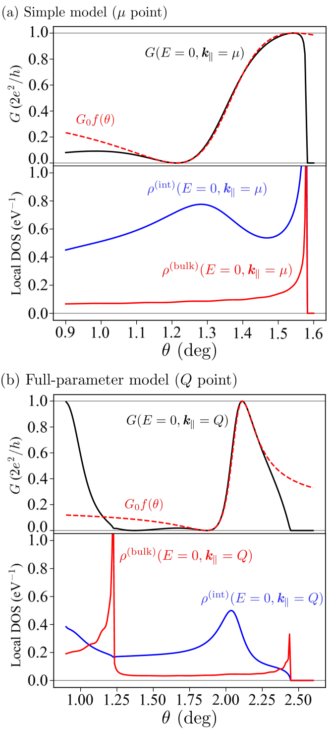
In the following, we demonstrate that the vanishing -resolved conductance argued in the previous section is attributed to the Fano resonance by the interface-localized level. We focus on the Fermi surface overlap center, i.e., for the simple model and for the full-parameter model, and plot the conductance against the twist angle . The results are shown in the upper panels of Figs. 9(a) and 9(b) for simple and full parameter models, respectively. In both cases, the conductance exhibits a sort of resonant behavior, where and 0 in Fig. 9 can be viewed as resonant and anti-resonant points, respectively. Here the maximum of the conductance is , since the number of conducting channels per spin of the non-twisted regions is 1 in the angle range of the figure.
The result implies that a resonance occurs between the bulk state of graphite and a interface-localized state. To identify associated interface states, we calculate the LDOS at the interface and also in the bulk region by using Eq. (26). In the numerical calculation, we introduce a finite middle region (Fig. 6) containing unit cells (100 graphene layers). We define the interface/bulk LDOS by
| (27) | |||
| (28) |
Here stands for trace over the wave bases belonging to the top graphene layer of the lower graphite, and the bottom layer of the upper graphite. The runs over the complementary bases in the middle part, which are not included in .
The lower panel of Fig. 9(a) shows the angle dependence of and with and in the simple model. We normalized to the value per two graphene layers, to be directly compared with . The exhibits a broad peak centered at , which indicates the emergence of an interface-localized state. For the full-parameter model, similarly, a peak of appears at as seen in Fig. 9(b). In both models, the bulk LDOS does not show a peak at the corresponding positions.
Generally, a system with weakly-coupled continuum and discrete spectra shows the Fano resonance [70], which is characterized by an asymmetric line shape in the system’s response. In twisted graphite, the emergent interface-localized state is considered to be a discrete state, while the bulk state contributes to a continuum spectrum. The transmission probability should then be given by the Fano function as a function of the twist angle,
| (29) |
where represents the broadening of the discrete state, is approximately equal to the position of the discrete state, and determines the asymmetry of the peak.
Here we fit the conductance curve by the Fano function , and plot the obtained curves with red dashed lines in Figs. 9(a) and 9(b). We employ the parameters , , for the simple model, and , , for the full-parameter model. The amplitude parameter is taken as for the correct peak height. In both cases, we see a fairly nice fitting with in a wide range of the twist angle. Also the obtained nearly coincides with the peak position of the interface LDOS-curve, which corresponds to the position of the discrete level. Regarding this good agreement, we conclude that the dip-and-peak structure of the perpendicular conductivity is attributed to the Fano resonance.
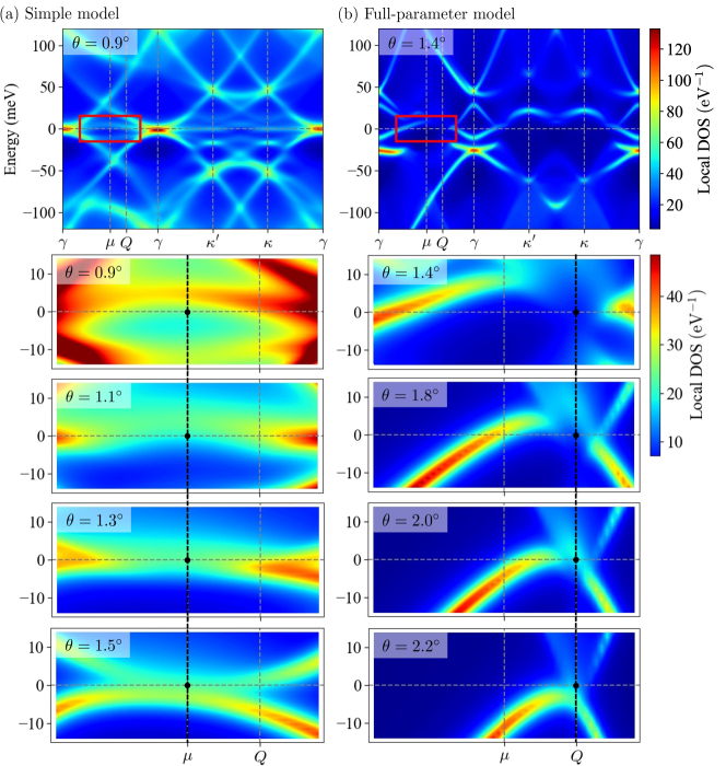
Finally, we demonstrate that the interface-localized state, which induces the Fano resonance, is a manifestation of a flat-band-like structure inherited from TBG. Here we compute the interface LDOS over a wide range of energy and momentum to identify the energy band associated with the interface-localized state. In the top panel of Fig. 10(a), we show the density plot of in the simple model with . A spectral broadening is introduced for the sake of visibility. Most of bright lines observed in the figure do not appear in the bulk LDOS (not shown), indicating that these lines correspond to the interface bands. The nearly-horizontal branch located at the energy of is the remnant of the flat band. Indeed, if we ignore the hopping parameters and retaining only and , the band becomes perfectly flat at [29].
The second top panel in Fig. 10(a) shows a magnified plot in the low-energy region, indicated by the red rectangle in the top panel. The third and lower panels are corresponding plots for different twist angles. When we increase the twist angle , the nearly flat band is lowered and traverses the point (indicated by a black dot) around . This corresponds to the interface LDOS peak in Fig. 9(a). Figure 10(b) presents similar plots for the full-parameter model. We observe that the flat band obtains some dispersion, yet it still persists in the low-energy region indicated by the red rectangle. In increasing the twist angle, the high-amplitude part crosses the point, and this causes the interface LDOS peak in Fig. 9(b).
VI Conductivity peak near 21.8∘
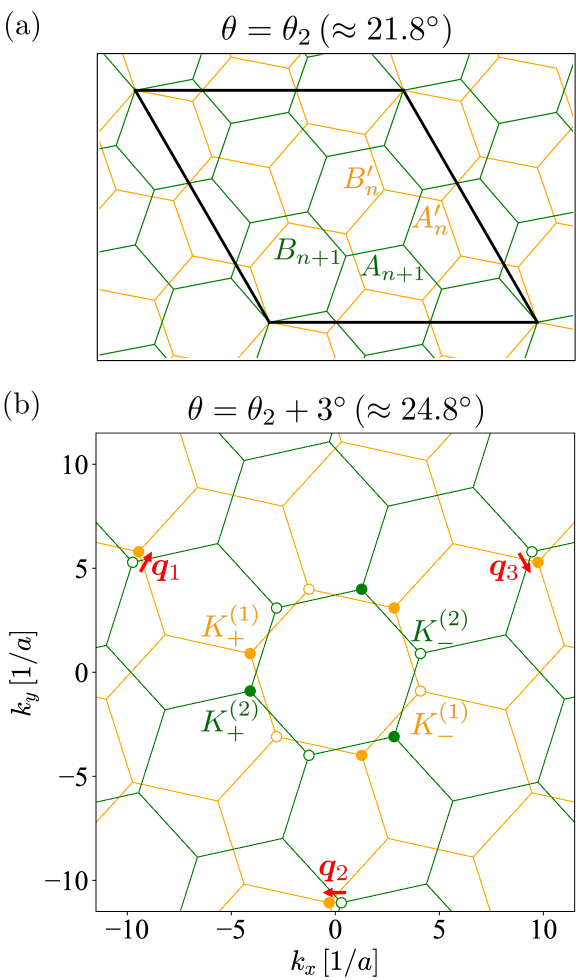
While we considered the small twist angle regime in the preceding sections, the coherent interlayer transport occurs also at other commensurate angles. In this section, we examine the perpendicular conductivity near the second commensurate angle , where the honeycomb lattices become exactly periodic with the unit cell as shown in Fig. 11(a) [71; 72; 73]. The interlayer transport in twisted graphene layers was theoretically investigated in the incoherent transport regime, and the conductivity enhancement at the commensurate angles was predicted [46]. Recent experiments reported a sharp conductance peak at in variable-angle graphite devices [51; 52; 53]. In the following, we describe the qualitative angle-dependent behavior near , by employing the same theoretical approach adopted in the previous section.
The interlayer coupling across the twisted interface near can be captured by a similar model to Eq. (3) for . Figure 11(b) shows the -space diagram for , which is near , where yellow and green honeycomb lattices represent the extended Brillouin zones for lower and upper graphite. As in Fig. 5(b), we define as the smallest separations between the corner points of upper and lower layers. Note that the ’s vanish at . These three vectors determine the moiré superperiod when is slightly away from , giving the smallest Fourier components in the interlayer Hamiltonian [74; 75].
When the lattice relaxation is neglected, the interlayer coupling magnitude associated with the ’s is given by , where is the -space position of the corresponding corner point, and the function is the Fourier transform of the interlayer hopping amplitude [46; 74; 75]. In the case of [Fig. 5(b)], is the point, giving the coupling magnitude of with . This leads to the simplest interlayer coupling Hamiltonian for TBG, which is Eq. (5) with and replaced by [1]. Note that the difference between and in Eq. (5) is introduced to effectively describe the lattice relaxation, which is only effective in the small regime.
In , the corner points are located at distance from the origin, resulting in an interface coupling matrix of [75],
| (30) |
The coupling amplitude is much smaller than for , as the Fourier transform is a decaying function. While the value of this factor strongly depends on the details of the model [72; 1; 75], here we employ , which is extracted from the tight-binding hopping model fitted to the LDA calculation [47; 76; 51]. In Appendix B, we evaluate by an alternative approach using the first-principles band calculation for the commensurate TBG of , to obtain the parameter of the same order.
Another important difference from is that the twisted interface of hybridizes electronic states at the opposite valleys, and , as seen in Fig. 11(b). As a result, pseudo-spin chirality of the Bloch electron is inverted between the two layers, and and in Eq. (3) are replaced by
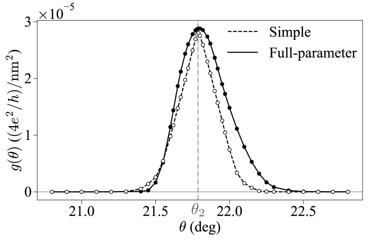
| (31) |
By using the Hamiltonian Eq. (3) with Eqs. (30) and (31), we calculate the electrical conductivity in the same manner as in the small-angle cases. The resulting contact conductivity near is shown in Fig. 12. For both simple and full-parameter models, we see that peaks around the commensurate angle . Since the interlayer coupling is perturbative, the multiple interlayer-scattering processes in the Green’s function are negligible, so that the transmission is dominated by the first-order hopping process. Therefore, is approximately proportional to , leading to the relationship . It should be noted that, in this high twist angle regime, no interface-localized states appear near , and hence the resonant behavior does not occur in the conductivity unlike in the low-angle regime. The sharp conductance peak at is qualitatively explained by the Fermi surface overlap at the remote point in Fig. 11(b).
The commensurate conductance peak at was experimentally observed in twisted interfaces between graphite and graphite [51], graphite and graphene [54], and graphene and graphene [53]. Our calculation in Fig. 12 roughly reproduces the order of magnitude of the interface conductivity in the graphite-graphite device [51], which is close to our situation. It should be noted that the interface transport in real devices has also a considerable contribution from the phonon-mediated hopping, which gives a smooth background mildly depending on the angle [47; 51].
VII Conclusion
We have developed a theoretical method to describe the transport in twisted 3D systems by using the recursive Green’s function approach. By using the formulation, we calculated the perpendicular conductivity in the twisted graphite. The calculated conductivity exhibits a nonmonotonic dip-and-peak structure against the twist angle, due to vanishing transmission at the overlap center of the Fermi surfaces. By examining the LDOS spectrum, we revealed that the drop of the conductance is caused by the Fano resonance between the bulk state and the interface-localized state, which is the remainder of a flat band of TBG. We also calculated the perpendicular conductivity at the twist angles around the second commensurate angle , and find a sharp peak around , which is consistent with experimental observation [51; 53].
Although we limited our argument to the twisted junction of two graphite pieces in this paper, the proposed formulation is applicable to diverse twisted systems. For instance, we can consider a system composed of two twisted interfaces with an -layer graphite in the middle section. There we anticipate the emergence of localized states in the middle section depending on its thickness , leading to complex resonances in the out-of-plane conductance through a similar mechanism. We can also extend our analysis to systems incorporating numerous twisted interfaces, including 3D graphite spirals [29; 77] and alternating twisted multilayer graphenes [78; 32]. This applies not only to graphitic materials; the formulation can be effectively extended to explore twisted interfaces of diverse metallic and superconducting materials. Applying the present method to study the perpendicular electronic transport in these systems would be intriguing future research.
Appendix A Recursive Green’s function method
In the present appendix, we explain the recursive Green’s function method [60; 68] to calculate the Green’s function of Eq. (20), . Each block of the Green’s function can be calculated from lower (upper) Green’s functions (), as shown below. Starting from the lower bulk Green’s function , the lower Green’s functions are computed by recursive relations
| (32) |
where . Similarly, from the upper bulk Green’s function , the upper Green’s functions can be gained by equations
| (33) |
where . Finally, we can obtain the full Green’s function by recursions
| (34) |
where .
Appendix B Alternative estimation of interlayer coupling
The interlayer coupling parameter , which determines the magnitude of the conductivity at the commensurate angle , is highly dependent on the detail of a model under consideration. In Sec. VI, we adopted the value of , which is extracted from the tight-binding hopping model fitted to the LDA calculation [47; 76; 51]. Here, we give an alternative evaluation of the parameter based on the band calculation of TBG at in two different methods, the effective continuum model and the density functional theory (DFT).
In the continuum model, we can calculate the energy bands of TBG with by the following Hamiltonian
| (35) |
Here the upper and lower diagonal blocks are the Dirac Hamiltonian of monolayer graphene at (lower layer) and (upper layer), respectively. Here, note that the interface of hybridizes opposite valleys as explained in Sec. VI. is the set of the Pauli matrices.
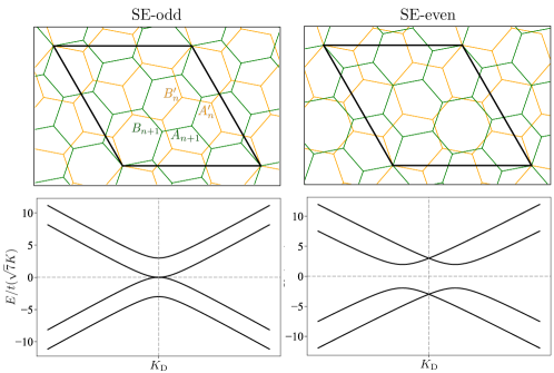
The off-diagonal block is the position-dependent interlayer potential given by Eq. (30). When the twist angle is slightly shifted from , the interlayer coupling slowly modulates as a function of position , where the corresponding moiré period is defined by with and . Then, the local Hamiltonian with a fixed corresponds to a commensurate TBG exactly at with a particular interlayer translation. In Fig. 13, we show the calculated energy bands at and , which correspond to the SE (sublattice exchange)-odd and SE-even structures, respectively [72]. Here the vertical axes is scaled by .
We can directly compare the band structure of Fig. 13 with the corresponding DFT band calculation [79]. By comparing the band splitting, we obtain , which has the same order as adopted in the main text. In the case of , the conductivity shown in Fig. 12 is enhanced by a factor of three, approximately, noting that the conductivity is nearly proportional to .
Acknowledgements.
This work was supported by JSPS KAKENHI Grants No. JP23KJ1497, No. JP20K14415, No. JP20H01840, No. JP20H00127, No. JP21H05236, and No. JP21H05232, and by JST CREST Grant No. JPMJCR20T3, Japan.References
- Bistritzer and MacDonald [2011] R. Bistritzer and A. H. MacDonald, Proc. Natl. Acad. Sci. U.S.A. 108, 12233 (2011).
- Cao et al. [2018a] Y. Cao, V. Fatemi, S. Fang, K. Watanabe, T. Taniguchi, E. Kaxiras, and P. Jarillo-Herrero, Nature 556, 43 (2018a).
- Cao et al. [2018b] Y. Cao, V. Fatemi, A. Demir, S. Fang, S. L. Tomarken, J. Y. Luo, J. D. Sanchez-Yamagishi, K. Watanabe, T. Taniguchi, E. Kaxiras, et al., Nature 556, 80 (2018b).
- Khalaf et al. [2019] E. Khalaf, A. J. Kruchkov, G. Tarnopolsky, and A. Vishwanath, Phys. Rev. B 100, 085109 (2019).
- Mora et al. [2019] C. Mora, N. Regnault, and B. A. Bernevig, Phys. Rev. Lett. 123, 026402 (2019).
- Carr et al. [2020] S. Carr, C. Li, Z. Zhu, E. Kaxiras, S. Sachdev, and A. Kruchkov, Nano Lett. 20, 3030 (2020).
- Hao et al. [2021] Z. Hao, A. M. Zimmerman, P. Ledwith, E. Khalaf, D. H. Najafabadi, K. Watanabe, T. Taniguchi, A. Vishwanath, and P. Kim, Science 371, 1133 (2021).
- Zhang et al. [2021] X. Zhang, K.-T. Tsai, Z. Zhu, W. Ren, Y. Luo, S. Carr, M. Luskin, E. Kaxiras, and K. Wang, Phys. Rev. Lett. 127, 166802 (2021).
- Park et al. [2021] J. M. Park, Y. Cao, K. Watanabe, T. Taniguchi, and P. Jarillo-Herrero, Nature 590, 249 (2021).
- Lei et al. [2021] C. Lei, L. Linhart, W. Qin, F. Libisch, and A. H. MacDonald, Phys. Rev. B 104, 035139 (2021).
- Nakatsuji et al. [2023] N. Nakatsuji, T. Kawakami, and M. Koshino, Phys. Rev. X 13, 041007 (2023).
- Koshino [2019] M. Koshino, Phys. Rev. B 99, 235406 (2019).
- Burg et al. [2019] G. W. Burg, J. Zhu, T. Taniguchi, K. Watanabe, A. H. MacDonald, and E. Tutuc, Phys. Rev. Lett. 123, 197702 (2019).
- Shen et al. [2020] C. Shen, Y. Chu, Q. Wu, N. Li, S. Wang, Y. Zhao, J. Tang, J. Liu, J. Tian, K. Watanabe, et al., Nat. Phys. 16, 520 (2020).
- Liu et al. [2020] X. Liu, Z. Hao, E. Khalaf, J. Y. Lee, Y. Ronen, H. Yoo, D. Haei Najafabadi, K. Watanabe, T. Taniguchi, A. Vishwanath, et al., Nature 583, 221 (2020).
- Haddadi et al. [2020] F. Haddadi, Q. Wu, A. J. Kruchkov, and O. V. Yazyev, Nano Lett. 20, 2410 (2020).
- Culchac et al. [2020] F. J. Culchac, R. R. Del Grande, R. B. Capaz, L. Chico, and E. S. Morell, Nanoscale 12, 5014 (2020).
- He et al. [2021] M. He, Y. Li, J. Cai, Y. Liu, K. Watanabe, T. Taniguchi, X. Xu, and M. Yankowitz, Nat. Phys. 17, 26 (2021).
- Szentpéteri et al. [2021] B. Szentpéteri, P. Rickhaus, F. K. de Vries, A. Márffy, B. Fülöp, E. Tóvári, K. Watanabe, T. Taniguchi, A. Kormányos, S. Csonka, et al., Nano Lett. 21, 8777 (2021).
- Tomić et al. [2022] P. Tomić, P. Rickhaus, A. Garcia-Ruiz, G. Zheng, E. Portolés, V. Fal’ko, K. Watanabe, T. Taniguchi, K. Ensslin, T. Ihn, et al., Phys. Rev. Lett. 128, 057702 (2022).
- Suárez Morell et al. [2013] E. Suárez Morell, M. Pacheco, L. Chico, and L. Brey, Phys. Rev. B 87, 125414 (2013).
- Park et al. [2020] Y. Park, B. L. Chittari, and J. Jung, Phys. Rev. B 102, 035411 (2020).
- Rademaker et al. [2020] L. Rademaker, I. V. Protopopov, and D. A. Abanin, Phys. Rev. Res. 2, 033150 (2020).
- Chen et al. [2021] S. Chen, M. He, Y.-H. Zhang, V. Hsieh, Z. Fei, K. Watanabe, T. Taniguchi, D. H. Cobden, X. Xu, C. R. Dean, et al., Nat. Phys. 17, 374 (2021).
- Li et al. [2022] S.-y. Li, Z. Wang, Y. Xue, Y. Wang, S. Zhang, J. Liu, Z. Zhu, K. Watanabe, T. Taniguchi, H.-j. Gao, et al., Nat. Commun. 13, 4225 (2022).
- Tong et al. [2022] L.-H. Tong, Q. Tong, L.-Z. Yang, Y.-Y. Zhou, Q. Wu, Y. Tian, L. Zhang, L. Zhang, Z. Qin, and L.-J. Yin, Phys. Rev. Lett. 128, 126401 (2022).
- Wu et al. [2014] J.-B. Wu, X. Zhang, M. Ijäs, W.-P. Han, X.-F. Qiao, X.-L. Li, D.-S. Jiang, A. C. Ferrari, and P.-H. Tan, Nature Communications 5, 5309 (2014).
- Wu et al. [2015] J.-B. Wu, Z.-X. Hu, X. Zhang, W.-P. Han, Y. Lu, W. Shi, X.-F. Qiao, M. Ijiäs, S. Milana, W. Ji, et al., ACS Nano 9, 7440 (2015).
- Cea et al. [2019] T. Cea, N. R. Walet, and F. Guinea, Nano Lett. 19, 8683 (2019).
- Liu et al. [2019] J. Liu, Z. Ma, J. Gao, and X. Dai, Phys. Rev. X 9, 031021 (2019).
- Tritsaris et al. [2020] G. A. Tritsaris, S. Carr, Z. Zhu, Y. Xie, S. B. Torrisi, J. Tang, M. Mattheakis, D. T. Larson, and E. Kaxiras, 2D Materials 7, 035028 (2020).
- Nguyen et al. [2022] V. H. Nguyen, T. X. Hoang, and J.-C. Charlier, J. Phys. Mater. 5, 034003 (2022).
- Park et al. [2022] J. M. Park, Y. Cao, L.-Q. Xia, S. Sun, K. Watanabe, T. Taniguchi, and P. Jarillo-Herrero, Nat. Mater. 21, 877 (2022).
- Wang and Liu [2022] J. Wang and Z. Liu, Phys. Rev. Lett. 128, 176403 (2022).
- Ledwith et al. [2022] P. J. Ledwith, A. Vishwanath, and E. Khalaf, Phys. Rev. Lett. 128, 176404 (2022).
- Zhang et al. [2023] S. Zhang, B. Xie, Q. Wu, J. Liu, and O. V. Yazyev, Nano Letters 23, 2921 (2023).
- Waters et al. [2023] D. Waters, E. Thompson, E. Arreguin-Martinez, M. Fujimoto, Y. Ren, K. Watanabe, T. Taniguchi, T. Cao, D. Xiao, and M. Yankowitz, Nature 620, 750 (2023).
- Britnell et al. [2012a] L. Britnell, R. V. Gorbachev, R. Jalil, B. D. Belle, F. Schedin, M. I. Katsnelson, L. Eaves, S. V. Morozov, A. S. Mayorov, N. M. R. Peres, et al., Nano Lett. 12, 1707 (2012a).
- Britnell et al. [2012b] L. Britnell, R. V. Gorbachev, R. Jalil, B. D. Belle, F. Schedin, A. Mishchenko, T. Georgiou, M. I. Katsnelson, L. Eaves, S. V. Morozov, et al., Science 335, 947 (2012b).
- Britnell et al. [2013] L. Britnell, R. V. Gorbachev, A. K. Geim, L. A. Ponomarenko, A. Mishchenko, M. T. Greenaway, T. M. Fromhold, K. S. Novoselov, and L. Eaves, Nat. Commun. 4, 1794 (2013).
- Kuzmina et al. [2021] A. Kuzmina, M. Parzefall, P. Back, T. Taniguchi, K. Watanabe, A. Jain, and L. Novotny, Nano Lett. 21, 8332 (2021).
- Mishchenko et al. [2014] A. Mishchenko, J. S. Tu, Y. Cao, R. V. Gorbachev, J. R. Wallbank, M. T. Greenaway, V. E. Morozov, S. V. Morozov, M. J. Zhu, S. L. Wong, et al., Nat. Nanotechnol. 9, 808 (2014).
- Ghazaryan et al. [2021] D. A. Ghazaryan, A. Misra, E. E. Vdovin, K. Watanabe, T. Taniguchi, S. V. Morozov, A. Mishchenko, and K. S. Novoselov, Appl. Phys. Lett. 118, 183106 (2021).
- Seo et al. [2022] Y. Seo, S. Masubuchi, M. Onodera, Y. Zhang, R. Moriya, K. Watanabe, T. Taniguchi, and T. Machida, Appl. Phys. Lett. 120, 083102 (2022).
- Koprivica and Sela [2022] D. Koprivica and E. Sela, Phys. Rev. B 106, 144110 (2022).
- Bistritzer and MacDonald [2010] R. Bistritzer and A. H. MacDonald, Phys. Rev. B 81, 245412 (2010).
- Perebeinos et al. [2012] V. Perebeinos, J. Tersoff, and P. Avouris, Phys. Rev. Lett. 109, 236604 (2012).
- Ahsan et al. [2013] S. Ahsan, K. M. Masum Habib, M. R. Neupane, and R. K. Lake, J. Appl. Phys. 114, 183711 (2013).
- Fang and Xiao [2021] H. Fang and M. Xiao, ACS Appl. Electron. Mater. 3, 2543 (2021).
- Fang et al. [2023] H. Fang, X. Huang, G. Li, and M. Xiao, Results Phys. 47, 106379 (2023).
- Koren et al. [2016] E. Koren, I. Leven, E. Lörtscher, A. Knoll, O. Hod, and U. Duerig, Nat. Nanotechnol. 11, 752 (2016).
- Li et al. [2018] H. Li, X. Wei, G. Wu, S. Gao, Q. Chen, and L.-M. Peng, Ultramicroscopy 193, 90 (2018).
- Inbar et al. [2023] A. Inbar, J. Birkbeck, J. Xiao, T. Taniguchi, K. Watanabe, B. Yan, Y. Oreg, A. Stern, E. Berg, and S. Ilani, Nature 614, 682 (2023).
- Chari et al. [2016] T. Chari, R. Ribeiro-Palau, C. R. Dean, and K. Shepard, Nano Lett. 16, 4477 (2016).
- Kim et al. [2013] Y. Kim, H. Yun, S.-G. Nam, M. Son, D. S. Lee, D. C. Kim, S. Seo, H. C. Choi, H.-J. Lee, S. W. Lee, et al., Phys. Rev. Lett. 110, 096602 (2013).
- Yu et al. [2020] Z. Yu, A. Song, L. Sun, Y. Li, L. Gao, H. Peng, T. Ma, Z. Liu, and J. Luo, Small 16, 1902844 (2020).
- Zhang et al. [2020] S. Zhang, A. Song, L. Chen, C. Jiang, C. Chen, L. Gao, Y. Hou, L. Liu, T. Ma, H. Wang, et al., Sci. Adv. 6, eabc5555 (2020).
- Soukoulis et al. [1982] C. M. Soukoulis, I. Webman, G. S. Grest, and E. N. Economou, Phys. Rev. B 26, 1838 (1982).
- MacKinnon et al. [1984] A. MacKinnon, L. Schweitzer, and B. Kramer, Surf. Sci. 142, 189 (1984).
- Ando [1991] T. Ando, Phys. Rev. B 44, 8017 (1991).
- McClure [1957] J. W. McClure, Phys. Rev. 108, 612 (1957).
- Slonczewski and Weiss [1958] J. C. Slonczewski and P. R. Weiss, Phys. Rev. 109, 272 (1958).
- Yabuki et al. [2016] N. Yabuki, R. Moriya, M. Arai, Y. Sata, S. Morikawa, S. Masubuchi, and T. Machida, Nat. Commun. 7, 10616 (2016).
- Koshino and Ando [2009] M. Koshino and T. Ando, Solid State Commun. 149, 1123 (2009).
- McCann and Koshino [2013] E. McCann and M. Koshino, Rep. Prog. Phys. 76, 056503 (2013).
- Moon and Koshino [2013] P. Moon and M. Koshino, Phys. Rev. B 87, 205404 (2013).
- Koshino et al. [2018] M. Koshino, N. F. Q. Yuan, T. Koretsune, M. Ochi, K. Kuroki, and L. Fu, Phys. Rev. X 8, 031087 (2018).
- Lewenkopf and Mucciolo [2013] C. H. Lewenkopf and E. R. Mucciolo, J. Comput. Electron. 12, 203 (2013).
- Landauer [1957] R. Landauer, IBM J. Res. Dev. 1, 223 (1957).
- Fano [1961] U. Fano, Phys. Rev. 124, 1866 (1961).
- Shallcross et al. [2008] S. Shallcross, S. Sharma, and O. A. Pankratov, Phys. Rev. Lett. 101, 056803 (2008).
- Mele [2010] E. J. Mele, Phys. Rev. B 81, 161405 (2010).
- Shallcross et al. [2010] S. Shallcross, S. Sharma, E. Kandelaki, and O. A. Pankratov, Phys. Rev. B 81, 165105 (2010).
- Fujimoto et al. [2022] M. Fujimoto, T. Kawakami, and M. Koshino, Phys. Rev. Res. 4, 043209 (2022).
- Koshino [2015] M. Koshino, New J. Phys. 17, 015014 (2015).
- Habib et al. [2013] K. M. M. Habib, S. S. Sylvia, S. Ge, M. Neupane, and R. K. Lake, Appl. Phys. Lett. 103, 243114 (2013).
- Wang et al. [2023] Z.-J. Wang, X. Kong, Y. Huang, J. Li, L. Bao, K. Cao, Y. Hu, J. Cai, L. Wang, H. Chen, et al., Nat. Mater. (2023).
- Burg et al. [2022] G. W. Burg, E. Khalaf, Y. Wang, K. Watanabe, T. Taniguchi, and E. Tutuc, Nat. Mater. 21, 884 (2022).
- Park et al. [2019] M. J. Park, Y. Kim, G. Y. Cho, and S. Lee, Phys. Rev. Lett. 123, 216803 (2019).