A first-principles approach to closing the “10-100 eV gap” for charge-carrier thermalization in semiconductors
Abstract
Since the 1960s and the first observations of radiation-induced disruption of electronic devices in space, the study of the effects of ionizing radiation on electronics has grown into an extensive field of its own. The present work is concerned with studying accurately the energy-loss processes that control the thermalization of hot carriers (electrons, holes, and/or electron-hole pairs) that are generated by high-energy radiation in wurtzite GaN, using an ab initio approach. Current physical models of the nuclear/particle physics community cover thermalization in the high-energy range (kinetic energies exceeding 100 eV), and the electronic-device community has studied extensively carrier transport in the low-energy range (below 10 eV). However, the processes that control the energy losses and thermalization of electrons and holes in the intermediate energy range of about 10-100 eV (which we define as the “10-100 eV gap”) are poorly known. The aim of this research is to close this gap. To this end, we utilize density functional theory (DFT) to obtain the band structure and dielectric function of GaN for energies up to about 100 eV. We also calculate charge-carrier scattering rates for the major charge-carrier interactions (phonon scattering, impact ionization, and plasmon emission), using the DFT results and first-order perturbation theory (Fermi’s Golden Rule/first Born approximation). With this information, we study the thermalization of electrons starting at 100 eV using the Monte Carlo method to solve the semiclassical Boltzmann transport equation. Full thermalization of electrons and holes is complete within 1 and 0.5 ps, respectively. Hot electrons dissipate about 90% of their initial kinetic energy to the electron-hole gas (90 eV) during the first 0.1 fs, due to rapid plasmon emission and impact ionization at high energies. The remaining energy is lost more slowly as phonon emission dominates at lower energies (below 10 eV). During the thermalization, hot electrons generate pairs with an average energy of 8.9 eV/pair (11-12 pairs per hot electron). Additionally, during the thermalization, the maximum electron displacement from its original position is found to be on the order of 100 nm.
I Introduction
In the study of ionizing radiation effects (including total ionizing dose (TID) and single-event effects (SEE)) in electronic devices and that of radiation detection (i.e., scintillators and semiconductor detectors), many computational tools have been developed to simulate particle transport and also the resulting possible material damage [1, 2, 3, 4]. These codes, developed by the nuclear/particle physics community, typically employ the binary collision and free-electron approximations. The primary assumption of the binary collision approximation is that the energetic projectile (an ion, for example) interacts via a series of independent two-body interactions with atoms in the material. As the energy decreases, this approximation begins to break down, as simultaneous interactions with multiple atoms occur. To handle this issue, these codes may consider nearly simultaneous interactions, allowing their use to be extended down below the keV range. At still lower energies ( 100 eV), the accuracy of the simulations comes into question as their results do not agree with experimental measurements, which yield deviations from monotonic response. For example, in Ref. [5], a monotonic decrease in the charge yield is measured with decreasing energy until energies reach the order of hundreds of eV. At this point, the charge yield apparently increases as the energy decreases from 100 eV to 70 eV. It is not clear what causes this phenomenon, but it is reasonable to suspect that electronic band structure effects may be partly to blame, and that inaccuracies of the simulations are associated with the use of the free-electron approximation. In addition, inaccuracies are likely caused by an inaccurate treatment of charge-carrier interactions.
The primary concern of this work is to study accurately the thermalization of hot carriers (electrons and/or electron-hole pairs) generated by high-energy radiation in semiconductors at energies below this threshold of 100 eV. Akkerman et al. have developed a code that employs the binary collision and free-electron approximations to simulate electron transport down to 20 eV (suggesting that the code can be extended down to 5 eV in some cases) [6]. Their approach, however, does not take the band structure and carrier-phonon scattering into account, which likely are critical for accurate simulation (especially for energies below 10 eV) [7].
To account for band structure effects, one may look to the electronic device community, which has done extensive work in developing codes to simulate carrier transport in the “low-energy” region (kinetic energies below 10 eV) [8, 9, 10, 11, 12]. Such simulations employ the full band structure in solving the semi-classical Boltzmann transport equation via the Monte Carlo (MC) method.
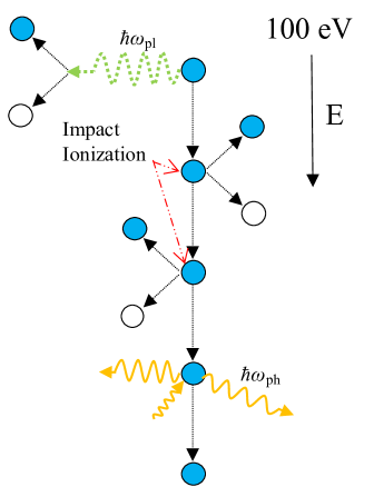
Between this low-energy region and what we call the “high-energy” region (kinetic energies exceeding 100 eV), there is an “intermediate-energy” range of about 10-100 eV, where the processes that control the energy losses and thermalization of electrons and holes are poorly known. We define this region as the “10-100 eV gap”. While only scant information on this topic is available, a major study by Pines showed that losses to plasmons are the dominant process [13]. We aim to study the scattering processes in this regime rigorously from first principles. In this effort, we include plasmon losses as well as impact ionization and phonon scattering in our model. To close this “10-100 eV gap”, we utilize the full-band approach and build up to 100 eV.
The energy-loss processes in the “10-100 eV gap” have been studied theoretically in the past: Rothwarf [14] and Kingsley and Ludwig [15] in phosphors, Alig et al. in semiconductors [16], Ausman and McLean in SiO2 [17]. These earlier studies followed Pines [18] in assuming that the main energy losses were due to plasmons. They considered also their decay into electron-hole pairs (EHPs), generation of EHPs via impact ionization processes, and final thermalization of the carriers via phonon scattering (see Fig. 1). However, these calculations were based on simplifying assumptions, such as the use of semi-empirical matrix elements and/or scattering rates and, most important, the free-electron model. Here we take a similar approach but use ab initio methods to compute both the band structure and the energy-loss and scattering rates. Indeed, it may be argued that the cutoff energy used in density functional theory (DFT), typically as large as 80 Ry, may be an excessive overestimation of the energy above which electrons can safely be taken as free. However, for electron kinetic energies lower than about 100 eV the ionic (pseudo)potentials represent a fraction of the total energy so large, 10% or more, that it cannot be ignored and the free-electron model cannot be expected to be accurate.
In addition to these early plasmon-based studies, with the prediction of single-event upset in 1962 [19], and the subsequent discoveries of other types of SEE [20, 21, 22, 23, 24] and TID, the study of ionizing radiation effects in Si-based devices has received much attention [20, 21, 22, 25, 26, 27]. Due to a relatively recent (within the past couple decades) surge in interest in wide band gap semiconductors [28, 29, 30], however, much work has been reported on ionizing radiation effects in materials such as SiC [31, 32, 33, 34], diamond, -Ga2O3 [35], and GaN [36, 37, 38]. As the use of wide band gap materials expands, there is a growing demand for implementation in space. For this work, we have chosen to focus on wurtzite GaN. In principle, however, the methods described in this paper can be applied to any semiconductor of interest.
GaN has a significantly larger band gap than Si (3.4 eV compared to 1.1 eV). The larger band gap gives it a much higher breakdown field (3.3 MV/cm compared to 0.3 MV/cm), which makes GaN a good candidate for high power electronics and extreme device scaling. GaN has a comparable, if not somewhat higher, electron mobility ( 1300-2000 cm2V-1cm-1 compared to 1440-1500 cm2V-1cm-1) due to its relatively small effective mass of 0.2 (the free electron mass). The electron drift velocity in GaN reaches a peak of - cm/s, while in Si, it saturates at cm/s. These characteristics have made GaN-based devices an increasingly important technology over the past couple decades.
As mentioned above, we use an ab initio approach (DFT) to obtain the electronic band structure of wurtzite GaN for bands reaching energies above 100 eV. Relevant charge-carrier scattering rates are calculated for the major charge-carrier interactions (phonon scattering, impact ionization, and plasmon emission), using the DFT results and first-order perturbation theory (Fermi’s Golden Rule/first Born approximation). With this information, the thermalization of electrons is simulated starting at 100 eV in a full-band MC (FBMC) code. A number of results are extracted, including the average carrier energy, energy distribution and position as a function of time, the average energy per generated pair, etc.
It is important to note that here we restrict our attention to low-dose irradiation at a low-dose-rate and, so, a low density of carriers. This restriction allows us to assume that the number of generated plasmons is small enough to leave their distribution at thermal equilibrium, so that we can ignore plasmon absorption. Similarly, the low density of carriers permits us to ignore also short-range carrier-carrier scattering.
II First-Principles Calculations
II.1 Electronic Band Structure
For this work, we use the DFT package Quantum ESPRESSO (QE) [39] for all ab initio calculations. Norm-conserving pseudopotentials [40] with PBE [41] exchange-correlation (XC) functionals are employed. The unit cell of wurtzite GaN is hexagonal with a space group of P63mc. We have utilized the experimentally measured lattice constants of and [42]. For the self-consistent calculation, we use a plane-wave cutoff energy of 120 Ry and a uniform Monkhorst-Pack grid of k points.
The FBMC simulation requires knowledge of the electronic band structure everywhere in the first Brillouin zone (BZ). We calculate the band structure for a total of 150 bands (up to 100 eV above the conduction band edge) for 3234 k points in the irreducible wedge of the BZ. These points are obtained by applying the 24 symmetry operations of wurtzite GaN to a uniform Monkhorst-Pack grid. Of the 150 bands, the first 18 are valence bands, representing the states of the 18 valence electrons of GaN (10 d- and 8 sp-electrons). The remaining 132 are conduction bands.
We note that according to x-ray photoemission spectroscopy measurements [43], below the states, the next valence state of GaN is the Ga state at eV (with respect to the valence band edge). To meet the requirement for energy conservation, a charge carrier would need to possess a minimum energy of 105.0 eV to excite an electron from this core state into the conduction bands. Taking momentum conservation into account as well, the threshold energy would be significantly higher. Thus, we may safely assume that core electrons do not play a significant role in the thermalization of charge carriers in the “10-100 eV gap” in GaN.
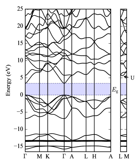
Figure 2 shows the band structure calculated along several high-symmetry lines of the BZ. The primary band gap is indicated by the shaded region labeled . Below this gap, all 18 valence bands are shown. These can be divided into three major groups. The group of the six highest-energy valence bands ( to 0 eV) represents sp states. Below these, there is a gap followed by a group of two more sp bands, which intersects a dense set of eight d bands. The final two d bands appear below these at around 15 eV. We note the detailed positions of these bands as they may vary with the pseudopotential and XC used.
| U | M | L | K | K | A | L | |
|---|---|---|---|---|---|---|---|
| This work | 7.18 | 8.00 | 7.80 | 9.42 | 9.68 | 10.49 | 11.10 |
| DFT-LDA [44] | 6.87 | 7.65 | 7.64 | 9.57 | 9.68 | 10.53 | 11.05 |
| Expt. [44] | 6.9 | 8.0 | 8.0 | 9.3 | 9.3 | 10.5-11.5 | 10.5-11.5 |
| Expt. [45] | 7.1 | 8.1 | 8.1 | 9.2 | 9.2 | - | - |
| Expt. [46] | 7.0 | 7.9 | 7.9 | 9.0 | 9.0 | - | - |
The DFT-calculated primary gap is 1.78 eV, which is slightly more than half of the measured value of 3.4 eV. This issue of underestimating the gap is a well-known problem associated with DFT. Many “solutions” have been proposed, including hybrid XC functionals, , and others. These have been highly successful in calculating the proper band gap, but their effects on transport properties are inconsistent [47]. Here we simply employ the “scissors” operator, shifting the conduction bands up by 1.62 eV to correct the gap. Additionally, using a curve-fitting technique, we calculate an electron effective mass of in the valley, which is somewhat smaller than the experimental value of [48]. It is, however, similar to the DFT result of 0.18 from Ref. [49].
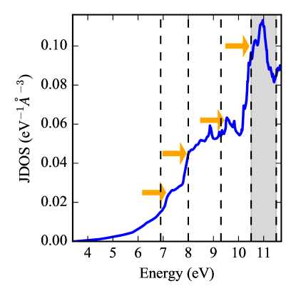
To assess the validity of the calculated band structure, we obtain the energies of direct transitions across the gap at certain symmetry points by calculating the joint density of states (JDOS):
| (1) |
where is the unit cell volume, is the conduction band index and in the valence band index. “Peaks” and “shoulders” of the JDOS occur for vertical transitions at BZ symmetry points. Similar peaks and shoulders occur in measured absorption/reflectivity spectra and dielectric function data, allowing one to make a direct comparison.
To evaluate the summation over the delta function in Eq. (1), we use Blöchl’s tetrahedron method [50]. It involves a discretization of the first BZ along the reciprocal lattice vectors (using the same uniform grid from above), filling it with “cube” elements. Each element is then divided into six tetrahedra. We then scan the BZ for all cubes which obey the energy-conservation requirement in Eq. (1). For all such cubes, the density of states (DOS) is evaluated by summing the contributions from each tetrahedron.
In Ref. [44], Lambrecht et al. measured reflectivity curves for wurtzite GaN. The resulting data yield several major peaks for which they identified corresponding transitions across the gap. A few of these major peaks in the reflectivity plot occur at 6.9 eV, 8.0 eV, 9.3 eV, and between 10.5 and 11.5 eV. In Fig. 3, we show the calculated JDOS; the above experimental energies and energy range have been marked with dashed lines. Arrows indicate characteristic peaks and shoulders. Qualitatively, we observe good agreement with Ref. [44], especially for the peaks at 8 eV and 11 eV.
| E2 (low) | B1 (low) | A1 (TO) | E1 (TO) | E2 (high) | B1 (high) | A1 (LO) | E1 (LO) | |
|---|---|---|---|---|---|---|---|---|
| This work | 16.89 | 39.94 | 63.35 | 65.39 | 66.31 | 82.34 | 86.56 | 86.73 |
| Theory [51] | 17.11 | 41.41 | 68.19 | 70.92 | 71.17 | 85.55 | 90.88 | 91.37 |
| Theory [52] | 17.73 | 41.78 | 67.07 | 70.42 | 71.79 | 89.27 | 92.74 | 93.85 |
| Theory [53] | 18.60 | 40.91 | 66.58 | 68.81 | 69.18 | 83.94 | ||
| Expt. [54] | 40.79 | 85.79 | 90.39 | |||||
| Expt. [55] | 17.85 | 66.08 | 69.55 | 70.55 | 91.13 | 92.12 |
We list in Table 1 the vertical transitions identified by Lambrecht et al. as well as those measured in Ref. [45] (via electron energy-loss spectroscopy) and Ref. [46] (via synchrotron ellipsometry). In addition, we include the DFT-LDA work by Lambrecht et al. [45]. In the table, ci and vi refer to conduction bands and valence bands, respectively, with representing the index of the band. For the valence band indices, corresponds to the highest valence band, and the index increases for deeper bands. For the conduction band indices, corresponds to the lowest conduction band and increases for higher bands. The point U refers to the satellite valley between L and M.
We note that for the above experimental work, the peaks associated with transitions have relatively large widths, leading to uncertainty in the true transition energies. This uncertainty leads, for example, to an apparent degeneracy at K and K in the experimental results, which does not agree with either our or the LDA calculations. We can therefore say only that the measured peaks give approximate energies of the transitions, and that the DFT data from this work and Ref. [44] are all in reasonably good agreement with these energies. Indeed, the largest discrepancy, occurring between our work and Ref. [46] for K, of 0.68 eV is not much larger than the discrepancies between the experimental results themselves (as large as 0.3 eV). Additionally, our calculated energy for this transition (9.68 eV) easily falls within the widths of the corresponding peaks (9.3 and 9.2 eV, respectively) in the plots of Refs. [44, 45]. Thus, we conclude that the use of the pseudopotential-XC functional combination of ONCV+PBE to calculate the band structure is justified.
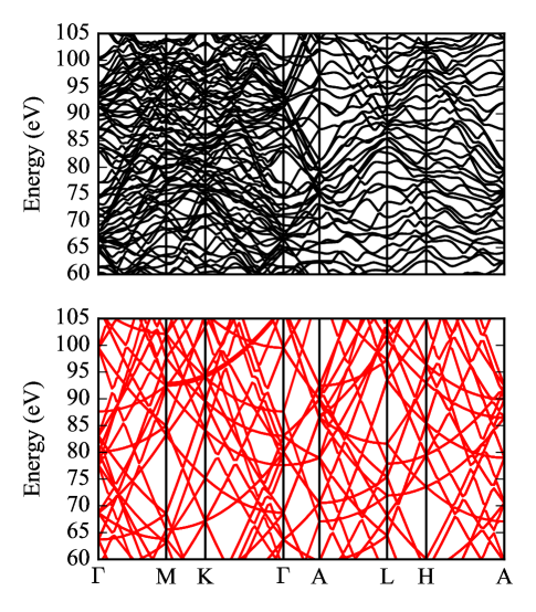
Lastly, we return briefly to the discussion on the use of DFT bands instead of free-electron bands. In Fig. 4, we plot both the DFT (conduction) bands (top frame) and the free-electron dispersion within the empty lattice approximation (bottom frame) on the upper end of the 10-100 eV energy range. We observe significant differences in both the density of the bands and their gradients (: the group velocity). As these deviations would affect the scattering rates, it is likely that they would also affect the charge-carrier thermalization rate. For accurate treatment, then, we use the DFT bands.
II.2 Phonon Dispersion
We utilize density functional perturbation theory (DFPT) within QE to evaluate the phonon dispersion. It calculates the lattice dynamical matrix for a given perturbation, , which can then be diagonalized to obtain the eigenvalues, , for each of the possible vibrational modes for a given crystal. Eigenstates are obtained for a set of 50 points in the irreducible wedge corresponding to an BZ mesh. The main purpose in obtaining the phonon dispersion is to evaluate the carrier-phonon interaction, which is covered below (see section II.3).
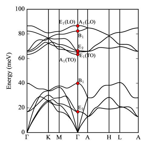
We plot the phonon dispersion calculated along several symmetry lines in the BZ in Fig. 5. The lowest three branches are acoustic, with the first two and the third known as transverse and longitudinal acoustic (TA and LA), respectively. The other nine branches are optical; all but the highest branch, which is longitudinal optical (LO), are transverse optical (TO).
The highest energy of the LO branch at (E1 (LO)) is 86.73 meV, which slightly underestimates the value measured by inelastic x-ray scattering of 90.4 meV [54] and that measured by Raman scattering of 92.1 meV [55]. In fact, in Table 2, several points on the phonon spectrum can be compared to those measured in Refs. [54, 55]: Whereas the first six branches seem to be in good agreement, the energies of the highest six are consistently underestimated by 3-5 meV. DFPT calculations from Refs. [51, 52] and frozen phonon calculations from Ref. [53] are also included in Table 2. We observe deviations among these theoretical works up to 5 meV, and deviations of similar magnitude are seen when comparing Refs. [51, 52, 53] with the experimental data. We conclude, therefore, that the deviations observed between our work and experiment are in line with the expected accuracy of DFPT calculations and other theoretical results.
II.3 Carrier-Phonon Interaction
In QE, the carrier-phonon interaction can be investigated by calculating the electron-phonon matrix elements using an included package called EPW (Electron-Phonon coupling using Wannier functions) [56, 57]. This program utilizes a Wannier-Fourier interpolation scheme to obtain the matrix elements on an arbitrarily fine mesh. The resulting matrix elements are given in the following form:
| (2) |
where is the initial electronic state, is the final state upon scattering with a phonon of wave vector and mode , and is the converged self-consistent potential from DFT.
We calculate the electron-phonon matrix elements for uniform grids of and for all valence bands (18 in total) and for the first 17 conduction bands. The reason for using only the first 17 conduction bands will become apparent in section III.2.3, where the rates for all scattering mechanisms are plotted together. In short, the rates of other scattering types (impact ionization and plasmon emission) exceed those of phonon scattering by a significant margin for intermediate energies (above 10 eV). Therefore, it is unnecessary to perform this calculation for energies much higher than 10 eV. We note, also, that as GaN is a polar material, we include in the calculation the long-range contributions to the carrier-phonon interaction, from polar optical phonons.
III Scattering Mechanisms
With the material properties determined, we now turn to the evaluation of the relevant charge-carrier interaction rates in GaN. For the study of hot-electron thermalization, we have chosen to consider phonon scattering, impact ionization, and valence-electron plasmon scattering. We will first discuss phonon scattering, and then we will introduce the energy-loss rate, which includes scattering from both impact ionization and plasmons.
III.1 Carrier-Phonon Scattering
To calculate the scattering rate between a carrier of wave vector k in band and a phonon of wave vector q of branch , we use first-order time-dependent perturbation theory (Fermi’s golden rule):
| (3) |
with
| (4) |
Here is the electron-phonon matrix element provided by EPW (section II.3), is the “final” wave vector of the scattered carrier, which has been mapped back into the first BZ, and is the final band of the scattered carrier. The numerical integration over the delta function is evaluated using a similar method to that reported by Fischetti and Laux [8]. This approach involves the use of the discretized BZ and identifying momentum- and energy-conserving cubes in the mesh. For such cubes, we employ Blöchl’s tetrahedron method to calculate the DOS, which is plugged into the summation of Eq. (3) in place of the delta function.
The electron-phonon scattering rates, evaluated for the lowest 17 conduction bands, are shown in Fig. 6 (top frame). The markers (blue) represent the rates calculated at 3234 points in the irreducible wedge. Over these markers, we have also plotted a solid line representing the average of the rates over equi-energy shells (yellow). At each energy, a spread, about the average, is observed in the rates, indicating that for much of this energy range, the rates have a relatively strong k-dependence. This k-dependence suggests that a purely energy-dependent rate is not sufficient to accurately simulate the scattering process in a FBMC simulation. Overall, the general shape and magnitude of the average compares well with those of Bertazzi et al. [11], who used an empirical pseudopotential method to generate the electronic band structure, the linear response method within density functional perturbation theory to obtain the phonon dispersion, and a deformation potential to produce the scattering rates.
The hole-phonon scattering rates are shown in the bottom frame of Fig. 6. Bertazzi et al. also calculated the hole-phonon rates, but only for the highest six valence bands, corresponding to energies up to 7-8 eV. Over this energy range, the general shape and magnitude of our hole-phonon scattering rates are in agreement with Ref. [11].
III.2 Impact Ionization and Plasmon Scattering
While electron- and hole-phonon scattering dominate in the low-energy regime, at higher energies, impact ionization and plasmon scattering become possible and more prevalent. From an experimental perspective, information about these scattering mechanisms is typically obtained via electron energy loss spectroscopy (EELS). The majority of the peaks and shoulders that appear in the resulting spectrum represent single electron excitations (impact ionization), while a few represent collective excitations of the valence electrons (valence-electron plasmons). These collective excitations, or plasmons, decay via Landau damping [58], which results in the creation of an EHP. We note that for both impact ionization and plasmon emission, we ignore excitons.
The total rate at which carriers scatter by these two mechanisms can be calculated using the dielectric function. This is so because the imaginary part of the inverse dielectric function (also known as the energy-loss function) is directly related to the EEL cross section. Here we include only plasmon emission, as the equilibrium plasmon occupation number is effectively zero (). In Chapter 2.6 of reference [59], FGR and the dissipation-fluctuation theorem [60, 61] are used to express the equilibrium scattering rate via the dielectric function as
| (5) |
Here is the energy-loss function, and and are the frequency and wave vector, respectively, of the resulting EHP or plasmon. We call this scattering rate the carrier energy-loss rate (ELR).
III.2.1 Calculation of the Dielectric Function
A number of techniques exist to obtain information about the EEL spectrum, and thus the loss function. In this work, we use time-dependent DFT via the code known as turboEELS [64], which is included in the QE package. It utilizes linearized time-dependent DFT within the Liouville-Lanczos approach to optical spectroscopies to calculate the EEL spectrum. First, we perform a standard ground-state DFT calculation with a Monkhorst-Pack grid. The result is then passed into turboEELS along with the wave vector, q, associated with the momentum transferred in the excitation process. Additionally, we use 1000 Lanczos iterations with a bi-constant extrapolation of the Lanczos coefficients up to 20000 and a Lorentzian broadening of 0.02 eV.
We repeat this calculation for a set of q and , so that an interpolation of the dynamic dielectric function () can be performed for any . Ideally, one would obtain these results on a mesh of q points, spanning the irreducible wedge of the BZ. This calculation, however, is a difficult task due to the computational cost of the calculation for each q. Instead, the dielectric function is calculated for a set of points along the first crystal axis (perpendicular to the c-axis) of the BZ. All dielectric function results shown below are from this data set. In section III.2.5, for a comparison, the dielectric function is also calculated for several points along the third crystal axis (parallel to the c-axis). Eq. (5) is then solved separately for each data set (perpendicular and parallel to the c-axis), assuming isotropy of the dielectric function. While the dielectric function is not isotropic for GaN, these two calculations can be used to provide an idea of how strongly the ELR depends on the anisotropy of the loss function.
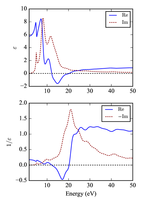
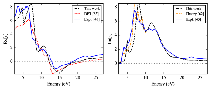
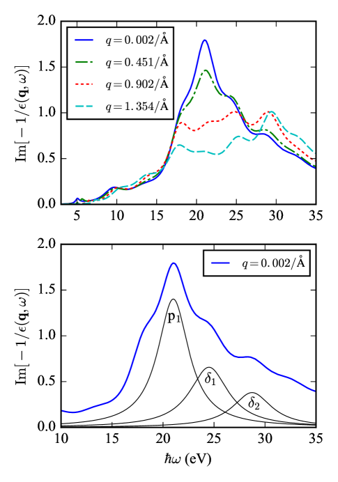
We first calculate for a small momentum transfer, , which corresponds to a magnitude of 0.0023 (Fig. 7). The real and imaginary parts of (Fig. 7, top frame) have been measured by spectroscopic ellipsometry [65, 66, 67, 62], and via reflectivity [44] and EELS measurements [45] using the Kramers-Kronig transformation. Looking first at Im[], our results yield three major peaks at approximately 5, 8 and 11.5 eV. In Fig. 8 (right frame) we show a direct comparison with experimental and theoretical works. For the EELS data of Ref. [45], major peaks occur at 4, 7 and between 10.5-13 eV, roughly corresponding to those from this work. Additional smaller peaks occur at 8, 9, 11 and 12.5 eV (in agreement with Refs. [44, 65, 66, 67, 62]), which do not appear in our results. We see that first-principles calculations of Im by Benedict et al. [62] were able to resolve the peaks at 8 and 9 eV, but they do not include the sharp peak at 4-5 eV.
For Re[] (left frame), we observe similar discrepancies between our work and experiment: Whereas our calculations seem to yield the major peaks, many of the more minor features do not appear in our results. We include a DFT calculation of Re[] from Ref. [63] in Fig. 8 (left frame). We observe that at energies eV the major peak magnitudes of Ref. [63], are significantly smaller than those of our work and Ref. [45]. Still, the peak locations seem to be in relatively good agreement. We note one key differences among these plotted data: the position of the zero of Re[] where the slope is positive. This zero occurs at 20.3 eV for our work, and at 22.9 eV for Ref. [63]. Both are higher than experiment ( 18-19 eV), but our result is roughly 12% closer. The importance of this zero will be discussed in the following section. Overall, we conclude that the accuracy of our calculations seems to be in line with the accuracy of other theoretical works.
The discrepancies between our calculations and measured dielectric function data most likely originate from the use of Lorentzian broadening in the turboEELS code. Broadening schemes, such as Gaussian and Lorentzian broadening, tend to smooth the results of a BZ integration, causing the details of the desired spectrum/data to be lost. In principle, one may adjust the broadening width to attempt to resolve these missing peaks, which we have done without success. Another option (that avoids changing the BZ integration scheme) is to increase the density of the Monkhorst-Pack grid. For a few points, we have incrementally increased the density beginning from and found convergence by . For further improvement one would need to change the integration scheme to a more accurate numerical technique such as the tetrahedron method [50] or Gilat-Raubenheimer method [68, 69]. Such an endeavor, however, would require significant effort, as one would need to change the turboEELS source code. For simplicity, we use the results from turboEELS without making any changes.
III.2.2 Plasmon Lifetime and Dispersion
Before calculating the carrier ELR, we first turn our attention to identifying the bulk plasmon peaks of wurtzite GaN in the loss function. In principle, by identifying these peaks, one may calculate the plasmon emission rate separately from the impact ionization rate. This approach allows one to treat the two phenomena separately within the FBMC code. The primary concern here is the lifetimes of the plasmons. As mentioned previously, plasmons decay via Landau damping, which results in the creation of an EHP. When the decay rate is sufficiently low, plasmons may live long enough in the system to be reabsorbed or slow the thermalization process. Dealing with these plasmons and their transport can significantly increase the complexity of the FBMC code.
To identify plasmon peaks in the loss function, one may first employ the so-called weak damping approximation [70]. Within this approximation, bulk plasmon energies can be found at zeroes of Re[] (where the slope is positive). Plasmons actually occur at complex zeros of the full complex dielectric function, but, when damping is weak, real zeros of the real part are a good approximation. When is small, this approximation tends to hold, but for larger , it breaks down. Additionally, there may be plasmon peaks for which the damping is strong enough so that the real part never vanishes on the real axis (even for small ).
In Fig. 7, Re goes through zero at 20.3 eV, which corresponds almost exactly with the largest peak in the loss function. We call this the primary plasmon peak (p1). It represents the major bulk plasmon predicted by the electron gas model,
| (6) |
to be at an energy of 21.7 eV. Here is the valence electron density ( and only) and is the free-electron mass. It originates from oscillations of the s and p valence electrons [71]. EELS data from Refs. [45, 71, 72, 73] yield a zero at a lower energy of 18-19 eV (Fig. 8, left frame). In addition to p1, two other peaks ( and ) are observed at 24 and 28 eV (Fig. 9). The locations of these peaks are in closer agreement with experiment [45, 71, 72, 73]. In a study of the loss functions of AlN and GaN, Dhall et al. [71] found that and are associated with collective excitations (plasmons) of the d electrons of Ga, and not single-particle excitations (impact ionization). As there are no zeroes of Re on the real axis at 24 and 28 eV (Fig. 7), one would not be able to identify these plasmons using the weak damping approximation.
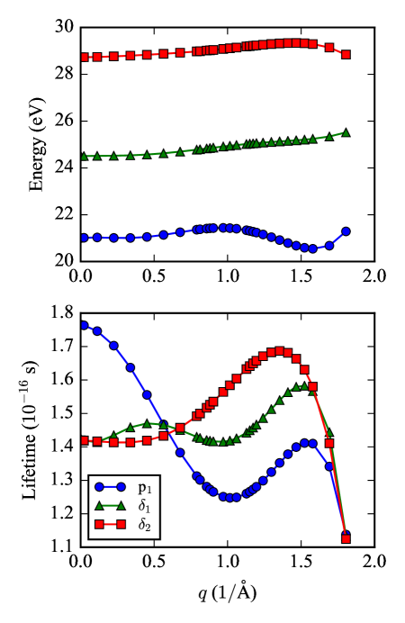
With the plasmon peaks identified, we fit Lorentzian curves to p1, , and , as shown in Fig. 9 (bottom frame). Several more Lorentzian curves, not shown in the figure, are fit to the surrounding peaks to improve the overall fit. Using this curve fitting, we track as a function of the peak positions, which yield the plasmon dispersion, and the full width at half maximum, which yields the plasmon lifetimes (Fig. 10). The top frame of Fig. 10 indicates that the plasmon energy of p1 is actually 21 eV and not 20.3 eV, where Re vanishes. This divergence suggests that the damping of p1 is not negligible.
The bottom frame of Fig. 10 shows that the plasmon lifetimes are all of order 10-16 s. We note that the lifetime for p1 is almost 50% larger than that of the delta peaks for small . As increases, the lifetime of p1 clearly decreases, suggesting that the damping increases. In contrast, the lifetime of the delta peaks is always short at small . We conclude that these magnitudes are short enough to assume immediate plasmon decay in the FBMC simulation. Therefore, we avoid the complexity of having to treat the plasmons separately from impact ionization, as discussed above.
In the top frame of Fig. 9, the loss function has a strong dependence on q, especially for the energy range from 16 eV to 35 eV. The shape and magnitude of these peaks change considerably, suggesting that the -dependence must be accounted for in the calculation of the ELR.
III.2.3 Electron and Hole Energy-Loss Rates
With the dielectric function calculated, we now evaluate the carrier ELRs. The numerical integration over the delta function in Eq. 5 is performed in a similar way as in section III.1. It begins with a search of the BZ for energy-and momentum-conserving cubes [8]. Here, however, there is an additional integration over . For each cube, we check for energy-conservation using a list of possible carrier energy losses, (from a discretization of the energy range from 0 to the kinetic energy of the incident carrier). If a given satisfies energy conservation in the cube, the DOS is calculated and included in the summation.
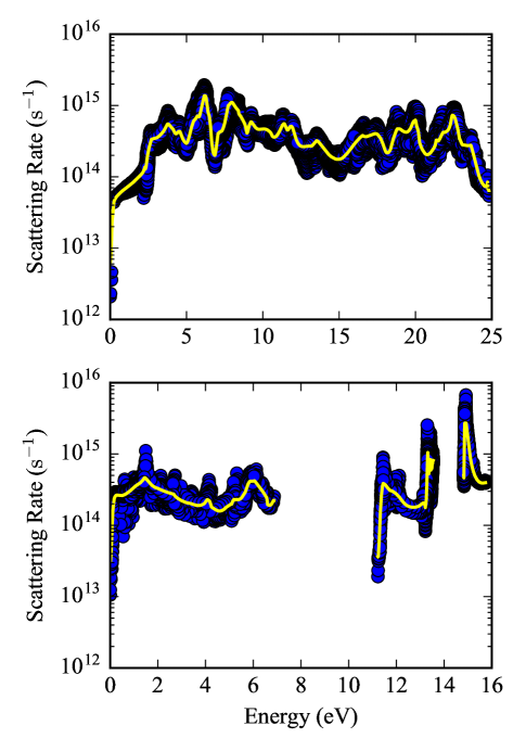
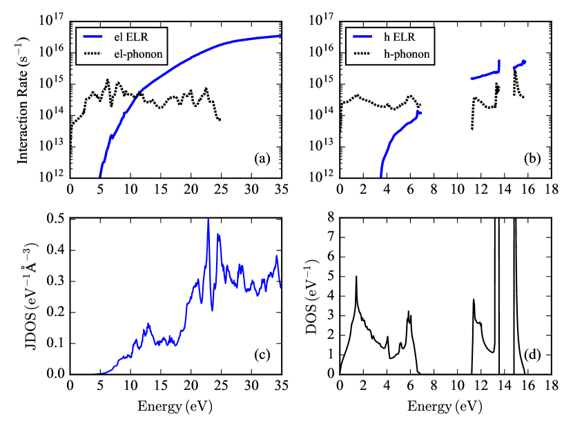
In Fig. 11 (a) and (b), we plot the calculated total electron and hole ELR, respectively. The phonon scattering rates for each are also shown. As previously mentioned, for electrons, phonon scattering dominates up to 10 eV above which the ELR dominates by 1-2 orders of magnitude. This fact makes the phonon interaction practically irrelevant above this point. For this reason, as discussed in section II.3, electron-phonon matrix elements above the 17th conduction band (25 eV) are not calculated. For the holes, phonon scattering is the major interaction mechanism up to the first gap at 7 eV. Just above 6 eV, impact ionization (ELR) reaches a similar magnitude, and it dominates for all higher energies.
The sharp peaks in the hole-phonon scattering rate, observed at 13.5 eV and 15 eV, originate from the incredibly dense d bands seen in Fig. 2. The DOS of these bands far exceeds the DOS of all other valence bands (Fig. 11 (d)) and even that of all conduction bands up to 100 eV. These d-band peaks lead to a significant jump in the JDOS at 17-18 eV (Fig. 11 (c)), caused by the onset of d-electron excitation (approximately the primary energy gap (3.4 eV) plus the depth of the first d bands). This jump accounts for the rather large magnitude of the electron ELR (1016-1017 s-1) in Fig. 11 (a), which will be discussed further in the following section.
The large ELRs shown in Fig. 11 may arguably raise some questions about the validity of the first Born approximation, which assumes that the wavefunction of the incident carrier is not appreciably affected by the scattering potential [74]. This concern has been addressed by Quinn and Ferrel [75, 76], Pines [13], Penn [77], and others who have calculated ELRs of the same magnitude. They have concluded that the electron energies at which the ELRs are high, are so large as to still render the broadening of electronic states acceptably small and that the use of perturbation theory is justified.
III.2.4 Alternative Methods for Calculating the Impact Ionization Rate
In order to identify separately collective (plasmon) and single-particle (impact ionization) contributions to the ELR obtained above, in this section, we present the carrier impact ionization rate (without plasmon scattering) calculated using two alternative methods to Eq. (5). These include the so called “constant matrix element” (CME) approximation and Kane’s random-k approximation [78], which are derived from the first Born approximation [79, 80]. Here we plot the results together with the ELR, which helps to assess the accuracy of the calculated ELR and to identify the energy regions in which impact ionization dominates.
As one might expect, the major assumption of the CME approximation is that the matrix element associated with the scattering process, , is a constant. We define this constant as the average value of the matrix element over all points in the BZ, all bands, and over both normal and Umklapp processes. This assumption emphasizes the idea that the matrix element plays a small role in determining the energy dependence of the ionization rate. Within this approximation, we write the impact ionization rate as [80]:
| (7) |
where
| (8) |
Here is the wave vector of the incident carrier in band , with energy . The wave vector is the crystal momentum of the final state of the incident carrier, and and are, respectively, the initial and final crystal momenta of the excited electron. As this excited electron begins in the valence band, we label the initial band as (v for valence band). The bands and are the final bands of the incident and excited particles, respectively (c for conduction band). The matrix element, , is the (anti)symmetrized screened Coulomb matrix element. For , is the lattice constant, is the static dielectric constant, and m is a number of order 1.
For the random-k approximation, we take Eq. (7) and employ further simplifications. The major assumption (along with those of CME) is that the JDOS available to the scattered (incident and excited) particles primarily controls the kinematics of the ionization process rather than momentum conservation [80]. In other words, this assumption suppresses momentum conservation in the ionization process. It holds when Umklapp processes dominate the pair production channel, causing momentum randomization. Within random-k, Eq. (7) becomes:
| (9) |
Here is the volume of the crystal primitive cell, is the energy of the “partner” electron (measured from the conduction band minimum) after jumping across the gap, is the energy of the “secondary” hole, is the initial energy of the “primary” particle, and (=’c’ or ’v’) is the total DOS at a given energy in either the valence band or conduction band.

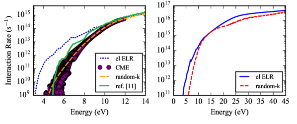
The CME and random-k results for electrons are shown in Fig. 12 (left frame). The CME rates are plotted for several k points spanning the irreducible wedge. As with phonon scattering (Fig. 6), we observe a spread in the rates, corresponding to momentum dependence. As energy increases, the spread narrows and converges to the random-k line. This convergence suggests that momentum dependence weakens for increasing energy and Umklapp processes become the dominant scattering process. A similar spread is observed in the work of Bertazzi et al. [11], who used an MC approach to solve the scattering rate equation within the Born approximation, considering both energy and momentum conservation, and including a dynamic matrix element. In Fig. 12, we show only the average ionization rate from Ref. [11], but the convergence to the random-k line is evident.
Additionally, we include in both frames of Fig. 12 the electron ELR. It too converges to the random-k results as energy increases. Between 15 and 20 eV, the ELR diverges from the random-k line as, it seems, plasmon emission begins to dominate. Eventually the two converge again at 45 eV, suggesting that impact ionization is again the major scattering mechanism. For low energies (below 10 eV), we note that the electron ELR data are orders of magnitude larger than the others. In 1956, Pines proposed the existence of acoustic plasmons that may also appear as excitations in the loss function [18]. It is possible that interactions with acoustic plasmons may be responsible for the discrepancy in question. From a practical perspective, this discrepancy is irrelevant as phonon scattering dominates in this energy regime. Indeed, we have artificially modified the ELR to more closely match the rates of Bertazzi et al. and found that this does not affect the MC simulation results in any significant way.
We note also that this low-energy discrepancy may be at least partly due to a numerical artifact in the Im, resulting from the use of Lorentzian broadening in turboEELS. Near the gap energy (3.4 eV), the loss function should go to zero, but instead, it remains nonzero down to much lower energies. As a result, Im is likely too large in this energy region causing a spurious increase in the ELR.
Interestingly, the random-k rates reach the same order of magnitude as the ELR (- s-1; eV). Because the random-k approximation assumes, by definition, that the impact ionization scattering process is controlled primarily by the JDOS, it can be concluded that the JDOS is the primary factor in driving the random-k results to this magnitude. This conclusion supports the claim, in the previous section, that the ELR are driven to such high magnitudes by the jump in the JDOS caused by d-electron excitations and the extremely large DOS of the d bands.
For holes (Fig. 13, left frame), we observe similar phenomena. All plotted rates converge to the random-k results as the energy increases. Additionally, we observe the same discrepancy between the hole ELR and the hole random-k results at low energies. We, again, attribute this to the possibility of acoustic plasmon scattering with a contribution from numerical artifacts in the calculation of the loss function. In practice, just as with electrons, phonon scattering dominates in this relatively low-energy regime, so there is no need to make any changes or improvements at this time.
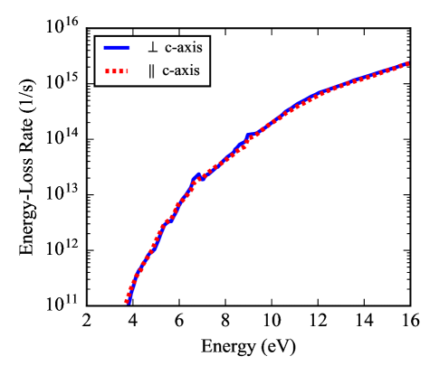
III.2.5 Dependence of the ELR on the Direction of q
Lastly, in this section, we come back to the issue of the anisotropy of the dielectric function in GaN and its effect on the ELR. As mentioned above, we have calculated the ELR using the dielectric function calculated perpendicular to the c-axis (“ELR ”, see Figs. 12 and 13) and that calculated parallel to the c-axis (“ELR ”). In Fig. 14, the two are plotted together for comparison. It is clear that there is excellent agreement between these rates. We conclude, then, that for the purposes of this work the anisotropy of the dielectric function does not significantly affect the ELR, and isotropy may be assumed without losing accuracy.
IV Full-Band Monte Carlo Simulation
In this section, we present our FBMC simulation. For the general setup, the use of a synchronous ensemble, and the scattering mechanism selection, we have followed the methods laid out by Jacoboni and Reggiani [81]. For the full band inclusion, we have followed Fischetti and Laux [8]. To establish the accuracy of the FBMC code and to further test the DFT data, we first calculate the low- and high-field transport characteristics. We then move to the simulation of the full thermalization of 100-eV electrons and the generated EHPs.
IV.1 Particle Initialization and Carrier Free Flight
To begin the MC simulation, we define the initial states of a set of charge carriers (electrons and/or holes). For the low- and high-field transport, these carriers are first assigned a random energy under the Fermi-Dirac distribution, using the rejection technique [82, 81]. For the hot-carrier thermalization, energies are assigned under a Gaussian distribution centered at 100 eV. Wave vectors are chosen, for each, by scanning the BZ mesh for all cubes that intersect the constant-energy surface , of the ith charge carrier. Each of these cubes is given a weight equal to the DOS at (via the tetrahedron method). A cube is then selected randomly by the rejection technique, using the weight as a probability distribution. A k within the cube is then chosen, such that . This selection is done by creating a “sub-mesh” within each cube and interpolating the energies at each sub-mesh point, beforehand, and storing them in a look-up table. The point with the closest energy to is selected.
After initialization, the carriers enter a “free flight”. For this calculation, we employ a synchronous ensemble technique [83, 81, 8]. We handle the free flight and the process of updating the particle state as is done in Ref. [8]. The one major exception is that we use a variable time step, d. The magnitude of d changes with each time step, as the maximum scattering rate changes throughout the simulation. We update d at the beginning of each free flight by obtaining the total scattering rate for each carrier and finding the maximum. From there, d is assigned a value equal to the inverse of the maximum scattering rate divided by 10. This approach is chosen due to the orders-of-magnitude change of the scattering rate over the course of the thermalization process. If one were to fix the time step based solely on the scattering rate at the beginning, it would take an exorbitantly long time to run the full thermalization process. This method is significantly faster and more efficient, but it would lose its efficiency if the scattering-rate magnitude changes very little during a simulation.
IV.2 Particle Scattering and the Selection of Final States
Following free flight, we determine whether each carrier scatters, using the techniques described in Ref. [81]. Once a scattering mechanism is chosen (or not), a final state of the incident carrier and, if applicable, the states of the excited carriers are selected.
Selecting a final state after a carrier-phonon scattering event proceeds much in same way that the scattering rate is calculated in section III.1. Following Ref. [8], we find all momentum- and energy-conserving cubes in the BZ (labeled with an index ), for all final bands . For each of these cubes, we calculate the density of final states at the final energy and assign a weight: , which is saved to a list. Using , one cube is chosen by rejection technique. A wave vector within the cube is then chosen, using the sub-mesh described in the previous section (IV.1), such that .
For plasmon emission, because we have assumed immediate decay of emitted plasmons into EHPs, the final state selection process is identical to that of impact ionization. This process is treated in two steps: first, the emission of a plasmon/generation of a pair, and second, the division of the EHP momentum and energy between the excited electron and hole.
For the first part, we employ a variation of the technique used for phonon scattering (Ref. [8]). We begin by taking the initial wave vector of the incident carrier, k, and calculating , where is the index for each cube in the BZ mesh, and kj is the point at the center of cube . We then generate a list of possible energy losses, . This list should span the energy range on which the dielectric function is calculated. In this case, the dielectric function is calculated from 0 to 100 eV, and a list of 200 energies is generated on this interval. For each of these energies, is calculated. The BZ is then searched for each cube in each band () containing . For these cubes, the density of states , at the final energy and a probability are calculated and saved to a list. The rejection technique is then utilized, as before, to select a cube and an energy loss, . The final wave vector of the incident particle is chosen, using the sub-mesh.
The final output of this section of code is the final state of the incident particle (energy and wave vector) and the energy and momentum of the EHP. To divide the pair energy and momentum between the excited electron and resulting hole, we utilize the random-k approximation. We consider a number of possible combinations () over the range from one extreme (electron absorbs all of the pair energy: ) to the other (). Here and are measured from the conduction band minimum and valence band maximum, respectively. For each combination, the probability is calculated and saved in a table. Here and are the total density of states at of the conduction bands and valence bands, respectively. The rejection technique is then used to select a combination (). With the energies selected, one simply finds all cubes that contain each energy and selects one, using rejection technique with the DOS as the probability distribution. Wave vectors within each cube are chosen using the sub-mesh method.
IV.3 Low- and High-Field Transport Characteristics
As mentioned above, to establish the accuracy of the FBMC code and to further test our DFT results, we first calculate the low- and high-field transport characteristics. We present these data in Figs. 15 and 16. Fields are directed along the -K symmetry line, for transport on the basal plane. In Fig. 15, we plot the calculated average electron drift velocity of this work with the results of a few theoretical works [9, 11, 84, 85, 86] and one experimental [87]. In all cases, we see a similar trend: a relatively steep slope at low fields followed by a peak, a gradual decrease, and eventual saturation. We extract a peak velocity of approximately cm/s, which agrees with Refs. [86, 85] and is in relatively good agreement with the experimental result: cm/s [87]. In contrast, both Fang et al. and Bertazzi et al. calculated peak velocities of about cm/s [9, 11], while a value of - cm/s is reported in Ref. [84]. Fang et al. used a very similar DFT approach to that used here, with ONCV pseudopotentials and LDA XC functionals. The peak velocity and other differences are likely attributable to the use of a different pseudopotential-XC combination [88].
For low fields (below 50 kV/cm), our results follow very closely those of Refs. [84, 86, 9], suggesting similar electron mobilities. From the slope at these low fields, we extract a mobility of 2000 cm2/(Vs). Indeed, this agrees well with the reported value of 1950 cm2/(Vs) from Ref. [9]. Both significantly exceed the experimentally measured value of 1300 cm2/(Vs) [89] (clearly seen by comparing the low-field slopes to that of Ref. [87] in Fig. 15). Fang et al. argue that this discrepancy is likely attributable to the lack of impurity and dislocation scattering in the theoretical models [9]. To this point, in Fig. 15, the slopes of Refs. [11, 85], in which ionized impurity scattering is included, are closer to experiment. Additionally, it is likely that inaccuracies in the band structure play a significant role. For example, our calculated electron effective mass underestimates the measure value (see section II.1), which one may predict will lead to a higher mobility. In a paper by Vitanov et al., in which they employed a non-parabolic model using experimentally calibrated material parameters (including the effective masses), an electron mobility of 1600 cm2/(Vs) is reported [90]. As this paper does not take impurity or defect scattering into account, it is clear that improvements in the band structure cause appreciable improvement in the predicted mobility.
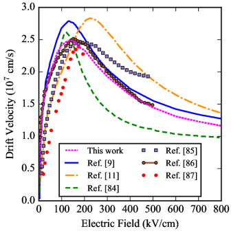
For the holes (Fig. 16, right frame), we observe a much smaller low-field slope, and we extract a mobility of 37 cm2/(Vs). This result is consistent with the relatively flat bands near the valence band maximum (Fig. 2). While it is considerably lower than results of other first-principles calculations, which found a value of 52 cm2/(Vs) [91], it is in excellent agreement with Hall-effect measurements of 31 cm2/(Vs) [92].
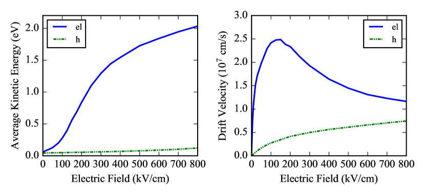
Following the peak, in all cases, the electron drift velocity decreases significantly and gradually reaches a steady-state saturation velocity. Chen et al. explain that saturation occurs as electrons fill the U and second valleys [93]. This work predicts a saturation velocity of approximately cm/s, which slightly exceeds that of Ref. [84]: cm/s. Results from Refs. [9, 11] are somewhat higher, settling down around cm/s. The hole drift velocity saturates to cm/s for a field strength of 1 MV/cm. As with the electrons, this is slightly lower than the value predicted by Bertazzi et el., who calculated a saturation velocity of 9.4 cm/s at the same field strength [11]. Saturation for holes occurs as they fill the M and A valleys.
The kinetic energy-field curves for electrons and holes are shown in the left frame of Fig. 16. We see that, initially, the electron energy remains nearly thermal until about 10 kV/cm, after which a gradual increase is observed. Between approximately 100-300 kV/cm, there is a sharper incline, which coincides with the peak electron drift velocity (large slope in the band structure). From 300-800 kV/cm, the slope of the energy-field curve gradually decreases as the average electron drift velocity saturates. These results agree well with those of Ref. [9]. The characteristic “S” shape is also reported by Kolnik et al. [94], who used an empirical pseudopotential method to calculate the band structure. The major discrepancy between our work and that of Ref. [94] is that electrons, in Ref. [94], remain near thermal energies up to much higher fields: up to about 50-100 kV/cm. This discrepancy is likely attributable to a difference in the electron effective mass (Ref. [94]: 0.2 , this work: 0.17 ). The larger effective mass reflects a smaller curvature of the band structure in the -valley. Additionally, their method includes ionized impurity scattering, which, as we have already seen, decreases the mobility significantly. This likely increases the total scattering rate enough to prevent significant kinetic energy gains for fields below 50-100 kV/cm.
IV.4 Hot Electron and Electron-Hole Pair Thermalization
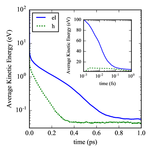
For the hot-electron thermalization simulation, we begin with a bulk wurtzite GaN crystal at a temperature of 300 K with no applied field. In such a system, at equilibrium, the electrons are at energies near the thermal level ( 40 meV). The sudden appearance of hot electrons is simulated by “injecting” a set of 1000 electrons with energies under a Gaussian distribution centered at 100 eV, as described in section IV.1.
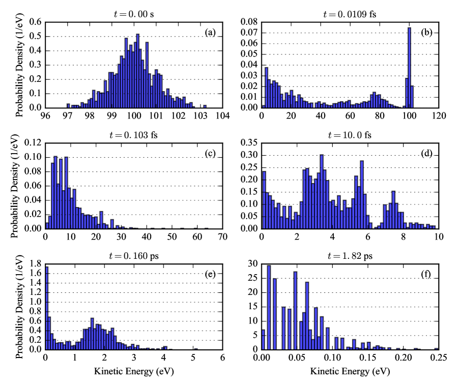
In Fig. 17, we plot the average electron and hole energies as a function of time, including the initial hot electrons and the generated EHPs. The time required for full electron thermalization is approximately 1 ps. For generated holes, thermalization is complete in roughly half the time. The initial steps of the simulation are difficult to see in the larger plot, due to the x-axis scale, so an inset figure is included (upper right), with a log time-scale. In this inset figure, we see that the electron energy drops sharply from 100 to 10 eV in 0.1-0.2 fs. This rapid decline of the kinetic energy per particle is caused by the fast transfer of the initial kinetic energy to generated carriers via the very fast emission of plasmons at these energies, with an emission rate of the order of 1016-1017 s-1 (Fig. 11).
The emitted plasmons tend to possess energies of 21, 24, and 28 eV, due to corresponding peaks in the loss function (Fig. 9). Figure 18 shows several snapshots of the energy distribution at certain times throughout the simulation. Initially (Fig. 18 (a)), the distribution is Gaussian, as expected. At 0.0109 fs (Fig. 18 (b)), we see that many electrons have already experienced one or more plasmon emission events. Peaks at roughly 80, 60, and 40 eV indicate losses in multiples of the abovementioned plasmon peak energies. The large number of electrons with energies below 20 eV correspond to generated EHPs. After 0.103 fs, we see, in Fig. 17, a sudden decrease in the thermalization rate. The energy distribution at this time indicates that most electrons possess energies below the lowest plasmon energy (Fig. 18 (c)), causing plasmon emission to cease and impact ionization and phonon scattering to be the primary scattering mechanisms. In Fig. 11, we see that with the dissipation of plasmon emission below 20 eV, the scattering rate drops an order of magnitude to 1015 s-1, which causes this decrease. After 10.0 fs (Fig. 18 (d)), the tail of the energy distribution, on the high end, no longer exceeds 10 eV. All electrons in the simulation, therefore, experience only phonon scattering.
Looking now at holes, we do not observe the same rapid energy decrease at the beginning of the simulation. Unless core states have been ionized by the original irradiation (a situation that we ignore here), hot holes do not possess sufficient energy to exceed the lowest plasmon frequency. Instead, holes tend to lose energy by a combination of impact ionization and phonon emission, leading to their much flatter slope in Fig. 17 (inset figure; fs). We note the increase in the average hole energy at the beginning of the simulation (inset figure; fs). Initially, no holes are included, and this increase simply corresponds to hole buildup as EHPs are generated. In the later stages of the process, which we can see in the larger frame of Fig. 17, the slope of the hole thermalization is greater than that of the electrons. The greater slope can be explained by the fact that hole-phonon scattering rates below 2.5 eV are roughly one order of magnitude larger than those of electrons (Fig. 6).
To observe where the energy goes in the thermalization process, the average number of generated pairs (per hot electron) is plotted along with the average energy lost to phonons as a function of time (Fig. 19). We see that during the initial stages of the simulation ( fs), most of the energy losses are to pair generation, as the energy lost to phonons is practically zero. At 10-14 s, phonon emission increases significantly, and the pair generation rate begins to flatten. These phonons will eventually decay, potentially resulting in temperature increases in the material.
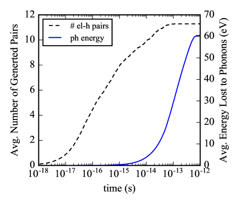
In this work, temperature effects are ignored, as we focus instead on the energy-loss processes in the “10-100 eV gap”. As phonons do not occur early on, while most electrons are still in the “10-100 eV gap”, it is not anticipated that temperature effects will significantly influence thermalization in this regime. Depending on the phonon density later in the process, temperature rises may be significant, affecting transport characteristics and device operation. Here we assume a low radiation dose and dose rate, resulting in a low hot electron density and, therefore, a low phonon density. This would lead to quick energy dissipation and removal from the system, and, therefore, to minimal temperature rises.
One may notice that 60% of the initial energy is lost to phonons by the end of the simulation. The other 40% can be accounted for by the ionization energy of each pair (number of pairs times the gap) plus some leftover kinetic energy of the electrons and holes. Eventually, this ionization energy will be lost to radiative (photons) and non-radiative (phonons) electron-hole recombination, and to Auger recombination. It is, however, presumed that the timescale for recombination will be significantly greater than a picosecond, and, therefore, it is not accounted for in this work. Indeed, the measurements of Jursenas et al. support this assumption, as the smallest recombination lifetimes are found to be of the order of a nanosecond [95].
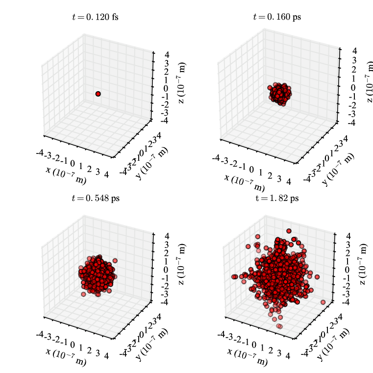
In addition to the energy distribution, we have also tracked the real-space positions of the simulated particles. This tracking allows us to analyze the real-space spread and average distance travelled during thermalization. We start the simulation with all electrons at the origin (Fig. 20). By the end (Fig. 20, bottom, right), the average distance travelled is on the order of 100 nm. As modern transistors have dimensions of approximately tens of nm, which continue to shrink, this result suggests that electrons generated by ionizing radiation will easily reach the boundaries of the device and may travel through several devices. This conclusion is in agreement with Weller et al. [96], who emphasize that this must be true for electronic equilibrium as a condition for proper device simulation and testing.
Lastly, we calculate the average energy required to generate an electron-hole pair, which is commonly referred to as the mean ionization energy. This number is important for understanding and determining the amount of free charge created by ionizing radiation/particles in electronic devices, especially in binary-collision codes. Furthermore, it is a parameter used in determining performance characteristics of semiconductors in radiation detection. By simply tracking the energies of EHPs as they are created, we calculate an average creation energy of 8.9 eV (with each hot electron generating 11-12 pairs, throughout the process). It is generally accepted that the mean ionization energy in a semiconductor is approximately equal to three times the bandgap ( eV, for GaN). On first glance, our result is reasonable, as it is within 14% of this guideline. A number of analytic approximations are also available to calculate this energy [97, 98, 99]. Using the empirical expression reported by Klein [99],
| (10) |
we calculate a value of 10.12 eV. A lower value of 9.59 eV has been found via electron-beam induced current measurements [100]. Even better (if not identical) agreement is observed with Ref. [101], in which a value of 8.9 eV is reported. Overall, we conclude that the calculated average creation energy is reasonable.
V Conclusions
We have presented a first-principles study of hot-electron and EHP thermalization in wurtzite GaN to close the “10-100 eV gap”. We have developed a FBMC code in which we have included plasmon emission and impact ionization, calculated using the full dynamic dielectric function, for accurate simulation of the thermalization processes in the intermediate energy range ( 10-100 eV). We also include phonon scattering for all valence bands (including the d bands) and for conduction bands up to a kinetic energy of 25 eV. We have found that, in agreement with Pines [13], plasmon-mediated processes dominate at high energy (during the initial 0.1 fs), impact ionization at intermediate energies (from 0.1 to 10 fs), and that phonons control the later stages of the thermalization (from 10 fs to full thermalization).
In addition to studying the time-scale, we have also investigated the length-scale (diffusion of hot carriers) and found that hot carriers travel an average distance of 100 nm. As others have found [96, 1], this distance easily exceeds the typical dimensions of modern electronic devices, consistent with the requirement to establish secondary electronic equilibrium during device simulation and testing. It is important to know how fast and how far these carriers decay as they may create defects in the crystal, cause unexpected and unwanted transients and shorts in FETs, and cause catastrophic failure of the device [1].
We have also calculated an average EHP creation energy of 8.9 eV/pair which agrees well with reported data. This number, also known as the mean ionization energy, is a critical parameter for the binary-collision codes of the nuclear/particle physics community. It also gives an idea of the amount of excess charge to expect, and, therefore, what kind of damage to predict.
Overall, this work provides the understanding, methods, and framework to study theoretically the full thermalization of charge carriers generated from a realistic streak of an ionizing particle in an electronic device.
VI Acknowledgements
We would like to thank A. Edwards and K. Goretta for organizing this research project and leading our many discussions. This work has been supported by the Air Force Office of Scientific Research: Award FA9550-21-0461, and through the Center of Excellence in Radiation Effects: Award FA9550-22-1-0012.
References
- Reed et al. [2015] R. A. Reed, R. A. Weller, M. H. Mendenhall, D. M. Fleetwood, K. M. Warren, B. D. Sierawski, M. P. King, R. D. Schrimpf, and E. C. Auden, Physical processes and applications of the Monte Carlo Radiative Energy Deposition (MRED) code, IEEE Trans. Nucl. Sci. 62, 1441 (2015).
- Agostinelli et al. [2003] S. Agostinelli, J. Allison, K. Amako, J. Apostolakis, H. Araujo, P. Arce, M. Asai, D. Axen, S. Banerjee, G. Barrand, F. Behner, L. Bellagamba, J. Boudreau, L. Broglia, A. Brunengo, H. Burkhardt, S. Chauvie, J. Chuma, R. Chytracek, G. Cooperman, G. Cosmo, P. Degtyarenko, A. Dell’Acqua, G. Depaola, D. Dietrich, R. Enami, A. Feliciello, C. Ferguson, H. Fesefeldt, G. Folger, F. Foppiano, A. Forti, S. Garelli, S. Giani, R. Giannitrapani, D. Gibin, J. Gómez Cadenas, I. González, G. Gracia Abril, G. Greeniaus, W. Greiner, V. Grichine, A. Grossheim, S. Guatelli, P. Gumplinger, R. Hamatsu, K. Hashimoto, H. Hasui, A. Heikkinen, A. Howard, V. Ivanchenko, A. Johnson, F. Jones, J. Kallenbach, N. Kanaya, M. Kawabata, Y. Kawabata, M. Kawaguti, S. Kelner, P. Kent, A. Kimura, T. Kodama, R. Kokoulin, M. Kossov, H. Kurashige, E. Lamanna, T. Lampén, V. Lara, V. Lefebure, F. Lei, M. Liendl, W. Lockman, F. Longo, S. Magni, M. Maire, E. Medernach, K. Minamimoto, P. Mora de Freitas, Y. Morita, K. Murakami, M. Nagamatu, R. Nartallo, P. Nieminen, T. Nishimura, K. Ohtsubo, M. Okamura, S. O’Neale, Y. Oohata, K. Paech, J. Perl, A. Pfeiffer, M. Pia, F. Ranjard, A. Rybin, S. Sadilov, E. Di Salvo, G. Santin, T. Sasaki, N. Savvas, Y. Sawada, S. Scherer, S. Sei, V. Sirotenko, D. Smith, N. Starkov, H. Stoecker, J. Sulkimo, M. Takahata, S. Tanaka, E. Tcherniaev, E. Safai Tehrani, M. Tropeano, P. Truscott, H. Uno, L. Urban, P. Urban, M. Verderi, A. Walkden, W. Wander, H. Weber, J. Wellisch, T. Wenaus, D. Williams, D. Wright, T. Yamada, H. Yoshida, and D. Zschiesche, Geant4—a simulation toolkit, Nucl. Instrum. Methods Phys. Res. A: Accel. Spectrom. Detect. Assoc. Equip. 506, 250 (2003).
- Allison et al. [2006] J. Allison, K. Amako, J. Apostolakis, H. Araujo, P. Arce Dubois, M. Asai, G. Barrand, R. Capra, S. Chauvie, R. Chytracek, G. Cirrone, G. Cooperman, G. Cosmo, G. Cuttone, G. Daquino, M. Donszelmann, M. Dressel, G. Folger, F. Foppiano, J. Generowicz, V. Grichine, S. Guatelli, P. Gumplinger, A. Heikkinen, I. Hrivnacova, A. Howard, S. Incerti, V. Ivanchenko, T. Johnson, F. Jones, T. Koi, R. Kokoulin, M. Kossov, H. Kurashige, V. Lara, S. Larsson, F. Lei, O. Link, F. Longo, M. Maire, A. Mantero, B. Mascialino, I. McLaren, P. Mendez Lorenzo, K. Minamimoto, K. Murakami, P. Nieminen, L. Pandola, S. Parlati, L. Peralta, J. Perl, A. Pfeiffer, M. Pia, A. Ribon, P. Rodrigues, G. Russo, S. Sadilov, G. Santin, T. Sasaki, D. Smith, N. Starkov, S. Tanaka, E. Tcherniaev, B. Tome, A. Trindade, P. Truscott, L. Urban, M. Verderi, A. Walkden, J. Wellisch, D. Williams, D. Wright, and H. Yoshida, Geant4 developments and applications, IEEE Trans. Nucl. Sci. 53, 270 (2006).
- Biersack and Haggmark [1980] J. P. Biersack and L. G. Haggmark, A Monte Carlo computer program for the transport of energetic ions in amorphous targets, Nucl. Instrum. 174, 257 (1980).
- Dozier and Brown [1981] C. M. Dozier and D. B. Brown, Effect of photon energy on the response of MOS devices, IEEE Trans. Nucl. Sci. 28, 4137 (1981).
- Akkerman et al. [2009] A. Akkerman, M. Murat, and J. Barak, Monte Carlo calculations of electron transport in silicon and related effects for energies of 0.02-200 keV, J. Appl. Phys. 106, 113703 (2009).
- Fang et al. [2019a] J. Fang, M. Reaz, S. L. Weeden-Wright, R. D. Schrimpf, R. A. Reed, R. A. Weller, M. V. Fischetti, and S. T. Pantelides, Understanding the average electron–hole pair-creation energy in silicon and germanium based on full-band Monte Carlo simulations, IEEE Trans. Nucl. Sci. 66, 444 (2019).
- Fischetti and Laux [1988] M. V. Fischetti and S. E. Laux, Monte Carlo analysis of electron transport in small semiconductor devices including band-structure and space-charge effects, Phys. Rev. B 38, 9721 (1988).
- Fang et al. [2019b] J. Fang, M. V. Fischetti, R. D. Schrimpf, R. A. Reed, E. Bellotti, and S. T. Pantelides, Electron transport properties of AlxGa1–xN/GaN transistors based on first-principles calculations and Boltzmann-equation Monte Carlo simulations, Phys. Rev. Appl. 11, 044045 (2019).
- Ghosh and Singisetti [2017] K. Ghosh and U. Singisetti, Ab initio velocity-field curves in monoclinic -Ga2O3, J. Appl. Phys. 122, 035702 (2017).
- Bertazzi et al. [2009] F. Bertazzi, M. Moresco, and E. Bellotti, Theory of high field carrier transport and impact ionization in wurtzite GaN. Part I: A full band Monte Carlo model, J. Appl. Phys. 106, 063718 (2009).
- Reaz et al. [2021] M. Reaz, A. M. Tonigan, K. Li, M. B. Smith, M. W. Rony, M. Gorchichko, A. O’Hara, D. Linten, J. Mitard, J. Fang, E. X. Zhang, M. L. Alles, R. A. Weller, D. M. Fleetwood, R. A. Reed, M. V. Fischetti, S. T. Pantelides, S. L. Weeden-Wright, and R. D. Schrimpf, 3-D full-band Monte Carlo simulation of hot-electron energy distributions in gate-all-around Si nanowire MOSFETs, IEEE Trans. Electron Devices 68, 2556 (2021).
- Pines [1956a] D. Pines, Collective energy losses in solids, Rev. Mod. Phys. 28, 184 (1956).
- Rothwarf [1973] A. Rothwarf, Plasmon theory of electron‐hole pair production: efficiency of cathode ray phosphors, J. Appl. Phys. 44, 752 (1973).
- Kingsley and Ludwig [1970] J. D. Kingsley and G. W. Ludwig, The efficiency of cathode‐ray phosphors: II . Correlation with other properties, J. Electrochem. Soc. 117, 353 (1970).
- Alig et al. [1980] R. C. Alig, S. Bloom, and C. W. Struck, Scattering by ionization and phonon emission in semiconductors, Phys. Rev. B 22, 5565 (1980).
- Ausman and McLean [1975] G. A. Ausman, Jr. and F. B. McLean, Electron-hole pair creation energy in SiO2, Appl. Phys. Lett. 26, 173 (1975).
- Pines [1956b] D. Pines, Electron interactions in solids, Can. J. Phys. 34, 1379 (1956).
- Wallmark and Marcus [1962] J. T. Wallmark and S. M. Marcus, Minimum size and maximum packing density of nonredundant semiconductor devices, Proc. IRE 50, 286 (1962).
- Kolasinski et al. [1979] W. A. Kolasinski, J. B. Blake, J. K. Anthony, W. E. Price, and E. C. Smith, Simulation of cosmic-ray induced soft errors and latchup in integrated-circuit computer memories, IEEE Trans.Nucl. Sci. 26, 5087 (1979).
- Wyatt et al. [1979] R. C. Wyatt, P. J. McNulty, P. Toumbas, P. L. Rothwell, and R. C. Filz, Soft errors induced by energetic protons, IEEE Trans. Nucl. Sci. 26, 4905 (1979).
- Guenzer et al. [1979] C. S. Guenzer, E. A. Wolicki, and R. G. Allas, Single event upset of dynamic rams by neutrons and protons, IEEE Trans. Nucl. Sci. 26, 5048 (1979).
- Soliman and Nichols [1983] K. Soliman and D. K. Nichols, Latchup in CMOS devices from heavy ions, IEEE Trans. Nucl. Sci. 30, 4514 (1983).
- Shiono et al. [1986] N. Shiono, Y. Sakagawa, M. Sekiguchi, K. Sato, I. Sugai, T. Hattori, and Y. Hirao, Single event effects in high density CMOS SRAMs, IEEE Trans. Nucl. Sci. 33, 1632 (1986).
- Shaneyfelt et al. [1991] M. R. Shaneyfelt, D. M. Fleetwood, J. R. Schwank, and K. L. Hughes, Charge yield for 10-keV X-ray and cobalt-60 irradiation of MOS devices, IEEE Trans. Nucl. Sci. 38, 1187 (1991).
- Oldham and McLean [2003] T. R. Oldham and F. B. McLean, Total ionizing dose effects in MOS oxides and devices, IEEE Trans. Nucl. Sci. 50, 483 (2003).
- Schwank et al. [2008] J. R. Schwank, D. M. Fleetwood, J. A. Felix, P. E. Dodd, P. Paillet, and V. Ferlet-Cavrois, Radiation effects in MOS oxides, IEEE Trans. Nucl. Sci. 55, 1833 (2008).
- Bose [2013] B. K. Bose, Global energy scenario and impact of power electronics in 21st century, IEEE Trans. Ind. Electron. 60, 2638 (2013).
- Franquelo et al. [2008] L. G. Franquelo, J. Rodriguez, J. I. Leon, S. Kouro, R. Portillo, and M. A. Prats, The age of multilevel converters arrives, IEEE Ind. Electron. Mag. 2, 28 (2008).
- Reynolds et al. [2012] M. A. Reynolds, D. Stidham, and Z. A. Alaywan, The golden spike: Advanced power electronics enables renewable development across NERC regions, IEEE Power Energy Mag. 10, 71 (2012).
- Akturk et al. [2017] A. Akturk, R. Wilkins, J. McGarrity, and B. Gersey, Single event effects in Si and SiC power MOSFETs due to terrestrial neutrons, IEEE Trans. Nucl. Sci. 64, 529 (2017).
- Witulski et al. [2018] A. F. Witulski, D. R. Ball, K. F. Galloway, A. Javanainen, J.-M. Lauenstein, A. L. Sternberg, and R. D. Schrimpf, Single-event burnout mechanisms in SiC power MOSFETs, IEEE Trans. Nucl. Sci. 65, 1951 (2018).
- Ball et al. [2020] D. R. Ball, K. F. Galloway, R. A. Johnson, M. L. Alles, A. L. Sternberg, B. D. Sierawski, A. F. Witulski, R. A. Reed, R. D. Schrimpf, J. M. Hutson, A. Javanainen, and J.-M. Lauenstein, Ion-induced energy pulse mechanism for single-event burnout in high-voltage SiC power MOSFETs and junction barrier Schottky diodes, IEEE Trans. Nucl. Sci. 67, 22 (2020).
- Zhou et al. [2019] X. Zhou, Y. Tang, Y. Jia, D. Hu, Y. Wu, T. Xia, H. Gong, and H. Pang, Single-event effects in SiC double-trench MOSFETs, IEEE Trans. Nucl. Sci. 66, 2312 (2019).
- Ma et al. [2023] H. Ma, W. Wang, Y. Cai, Z. Wang, T. Zhang, Q. Feng, Y. Chen, C. Zhang, J. Zhang, and Y. Hao, Analysis of single event effects by heavy ion irradiation of Ga2O3 metal–oxide–semiconductor field-effect transistors, J. Appl. Phys. 133, 085701 (2023).
- Fleetwood et al. [2022] D. M. Fleetwood, E. X. Zhang, R. D. Schrimpf, and S. T. Pantelides, Radiation effects in AlGaN/GaN HEMTs, IEEE Trans. Nucl. Sci. 69, 1105 (2022).
- Ives et al. [2015] N. E. Ives, J. Chen, A. F. Witulski, R. D. Schrimpf, D. M. Fleetwood, R. W. Bruce, M. W. McCurdy, E. X. Zhang, and L. W. Massengill, Effects of proton-induced displacement damage on gallium nitride HEMTs in RF power amplifier applications, IEEE Trans. Nucl. Sci. 62, 2417 (2015).
- Jiang et al. [2017] R. Jiang, E. X. Zhang, M. W. McCurdy, J. Chen, X. Shen, P. Wang, D. M. Fleetwood, R. D. Schrimpf, S. W. Kaun, E. C. H. Kyle, J. S. Speck, and S. T. Pantelides, Worst-case bias for proton and 10-keV X-ray irradiation of AlGaN/GaN HEMTs, IEEE Trans. Nucl. Sci. 64, 218 (2017).
- Giannozzi et al. [2009] P. Giannozzi, S. Baroni, N. Bonini, M. Calandra, R. Car, C. Cavazzoni, D. Ceresoli, G. L. Chiarotti, M. Cococcioni, I. Dabo, A. Dal Corso, S. de Gironcoli, S. Fabris, G. Fratesi, R. Gebauer, U. Gerstmann, C. Gougoussis, A. Kokalj, M. Lazzeri, L. Martin-Samos, N. Marzari, F. Mauri, R. Mazzarello, S. Paolini, A. Pasquarello, L. Paulatto, C. Sbraccia, S. Scandolo, G. Sclauzero, A. P. Seitsonen, A. Smogunov, P. Umari, and R. M. Wentzcovitch, QUANTUM ESPRESSO: a modular and open-source software project for quantum simulations of materials, J. Phys.: Cond. Matt. 21, 395502 (2009).
- Schlipf and Gygi [2015] M. Schlipf and F. Gygi, Optimization algorithm for the generation of ONCV pseudopotentials, Comput. Phys. Commun. 196, 36 (2015).
- Perdew et al. [1996] J. P. Perdew, K. Burke, and M. Ernzerhof, Generalized gradient approximation made simple, Phys. Rev. Lett. 77 18, 3865 (1996).
- Lagerstedt and Monemar [1979] O. Lagerstedt and B. Monemar, Variation of lattice parameters in GaN with stoichiometry and doping, Phys. Rev. B 19, 3064 (1979).
- Martin et al. [1994] G. Martin, S. Strite, A. Botchkarev, A. Agarwal, A. Rockett, H. Morkoç, W. R. L. Lambrecht, and B. Segall, Valence‐band discontinuity between GaN and AlN measured by x‐ray photoemission spectroscopy, Appl. Phys. Lett. 65, 610 (1994).
- Lambrecht et al. [1995] W. R. L. Lambrecht, B. Segall, J. Rife, W. R. Hunter, and D. K. Wickenden, UV reflectivity of GaN: Theory and experiment, Phys. Rev. B 51, 13516 (1995).
- Brockt and Lakner [2000] G. Brockt and H. Lakner, Nanoscale EELS analysis of dielectric function and bandgap properties in GaN and related materials, Micron 31, 435 (2000).
- Logothetidis et al. [1994] S. Logothetidis, J. Petalas, M. Cardona, and T. D. Moustakas, Optical properties and temperature dependence of the interband transitions of cubic and hexagonal GaN, Phys. Rev. B 50, 18017 (1994).
- Nielsen et al. [2021] D. Nielsen, M. Van de Put, and M. Fischetti, Investigating the use of HSE hybrid functionals to improve electron transport calculations in Si, Ge, Diamond, and SiC, in 2021 International Conference on Simulation of Semiconductor Processes and Devices (SISPAD) (2021) pp. 133–137.
- Drechsler et al. [1995] M. Drechsler, D. M. Hofmann, B. K. Meyer, T. Detchprohm, H. Amano, and I. Akasaki, Determination of the conduction band electron effective mass in hexagonal GaN, Jap. J. Appl. Phys. 34, L1178 (1995).
- Suzuki and Uenoyama [1996] M. Suzuki and T. Uenoyama, Strain effect on electronic and optical properties of GaN/AlGaN quantum‐well lasers, Journal of Applied Physics 80, 6868 (1996).
- Blöchl et al. [1994] P. E. Blöchl, O. Jepsen, and O. K. Andersen, Improved tetrahedron method for Brillouin-zone integrations, Phys. Rev. B 49 23, 16223 (1994).
- Bungaro et al. [2000] C. Bungaro, K. Rapcewicz, and J. Bernholc, Ab initio phonon dispersions of wurtzite AlN, GaN, and InN, Phys. Rev. B 61, 6720 (2000).
- Karch et al. [1998] K. Karch, J.-M. Wagner, and F. Bechstedt, Ab initio study of structural, dielectric, and dynamical properties of GaN, Phys. Rev. B 57, 7043 (1998).
- Gorczyca et al. [1995] I. Gorczyca, N. E. Christensen, E. L. Peltzer y Blancá, and C. O. Rodriguez, Optical phonon modes in GaN and AlN, Phys. Rev. B 51, 11936 (1995).
- Ruf et al. [2001] T. Ruf, J. Serrano, M. Cardona, P. Pavone, M. Pabst, M. Krisch, M. D’Astuto, T. Suski, I. Grzegory, and M. Leszczynski, Phonon dispersion curves in Wurtzite-structure GaN determined by inelastic X-ray scattering, Phys. Rev. Lett. 86, 906 (2001).
- Azuhata et al. [1995] T. Azuhata, T. Sota, K. Suzuki, and S. Nakamura, Polarized Raman spectra in GaN, J. Phys.: Condens. Matter 7, L129 (1995).
- Poncé et al. [2016] S. Poncé, E. R. Margine, C. Verdi, and F. Giustino, EPW: Electron-phonon coupling, transport and superconducting properties using maximally localized Wannier functions, Comput. Phys. Commun. 209, 116 (2016).
- Giustino et al. [2007] F. Giustino, C. M. L., and L. S. G., Electron-phonon interaction using Wannier functions, Phys. Rev. B 76, 165108 (2007).
- Landau [1946] L. Landau, On the vibrations of the electronic plasma, Acad. Sci. USSR. J. Phys. 10, 25 (1946).
- Nozieres and Pines [1999] P. Nozieres and D. Pines, Theory of Quantum Liquids (Westview Press, Perseus Books Group, Boulder, CO, 1999).
- Nyquist [1928] H. Nyquist, Thermal agitation of electric charge in conductors, Phys. Rev. 32, 110 (1928).
- Callen and Welton [1951] H. B. Callen and T. A. Welton, Irreversibility and generalized noise, Phys. Rev. 83, 34 (1951).
- Benedict et al. [1999] L. X. Benedict, T. Wethkamp, K. Wilmers, C. Cobet, N. Esser, E. L. Shirley, W. Richter, and M. Cardona, Dielectric function of wurtzite GaN and AlN thin films, Solid State Commun. 112, 129 (1999).
- Eljarrat et al. [2016] A. Eljarrat, X. Sastre, F. Peiró, and S. Estradé, Density functional theory modeling of low-loss electron energy-loss spectroscopy in wurtzite III-nitride ternary alloys, Microsc. Microanal. 22, 706 (2016).
- Timrov et al. [2015] I. Timrov, N. Vast, R. Gebauer, and S. Baroni, turboEELS - A code for the simulation of the electron energy loss and inelastic X-ray scattering spectra using the Liouville-Lanczos approach to time-dependent density-functional perturbation theory, Comput. Phys. Commun. 196, 460 (2015).
- Goldhahn et al. [2004] R. Goldhahn, C. Buchheim, V. Lebedev, V. Cimalla, C. Cobet, M. Rakel, N. Esser, U. Rossow, and D. Fuhrmann, Dielectric function and critical points of the band structure for hexagonal and cubic GaN and AlN, in BESSY - Annual Report 2004 (2004) p. 206.
- Kawashima et al. [1997] T. Kawashima, H. Yoshikawa, S. Adachi, S. Fuke, and K. Ohtsuka, Optical properties of hexagonal GaN, J. Appl. Phys. 82, 3528 (1997).
- Cobet et al. [2009] C. Cobet, R. Goldhahn, W. Richter, and N. Esser, Identification of van Hove singularities in the GaN dielectric function: a comparison of the cubic and hexagonal phase, Phys. Status Solidi (b) 246, 1440 (2009).
- Gilat and Raubenheimer [1966] G. Gilat and L. J. Raubenheimer, Accurate numerical method for calculating frequency-distribution functions in solids, Phys. Rev. 144, 390 (1966).
- Liu et al. [2017] B. Liu, S. G. Johnson, J. D. Joannopoulos, and L. Lu, Generalized Gilat–Raubenheimer method for density-of-states calculation in photonic crystals, J. Opt. 20, 044005 (2017).
- Hamann et al. [2020] P. Hamann, J. Vorberger, T. Dornheim, Z. A. Moldabekov, and M. Bonitz, Ab initio results for the plasmon dispersion and damping of the warm dense electron gas, Contrib. Plasma Phys. 60, e202000147 (2020).
- Dhall et al. [2018] R. Dhall, D. Vigil-Fowler, J. Houston Dycus, R. Kirste, S. Mita, Z. Sitar, R. Collazo, and J. M. LeBeau, Probing collective oscillation of d-orbital electrons at the nanoscale, Appl. Phys. Lett. 112, 061102 (2018).
- Benaissa et al. [2021] M. Benaissa, W. Sigle, I. Benabdallah, R. T. Elafandy, T. K. Ng, and P. A. van Aken, Optical properties of freestanding GaN nanomembranes using monochromated valence-EELS, Mater.s Sci. Eng. B 272, 115333 (2021).
- Sanchez et al. [2004] A. M. Sanchez, M. H. Gass, A. J. Papworth, P. Goodhew, and P. Ruterana, Nanoscale EELS analysis of InGaN/GaN heterostructures, Phys. Rev. B 70, 035325 (2004).
- Griffiths [1995] D. J. Griffiths, Introduction to Quantum Mechanics (Prentice Hall, Upper Saddle River, New Jersey, 1995).
- Quinn and Ferrell [1958] J. J. Quinn and R. A. Ferrell, Electron self-energy approach to correlation in a degenerate electron gas, Phys. Rev. 112, 812 (1958).
- Quinn [1962] J. J. Quinn, Range of excited electrons in metals, Phys. Rev. 126, 1453 (1962).
- Penn [1987] D. R. Penn, Electron mean-free-path calculations using a model dielectric function, Phys. Rev. B 35 2, 482 (1987).
- Kane [1967] E. O. Kane, Electron scattering by pair production in silicon, Phys. Rev. 159, 624 (1967).
- Sano et al. [1990] N. Sano, T. Aoki, M. Tomizawa, and A. Yoshii, Electron transport and impact ionization in Si, Phys. Rev. B 41 17, 12122 (1990).
- Fischetti et al. [1996] M. V. Fischetti, N. Sano, S. E. Laux, and K. Natori, Full-band-structure theory of high-field transport and impact ionization of electrons and holes in Ge, Si, and GaAs, J. Technol. Comput. Aided Des. 10, 1 (1996).
- Jacoboni and Reggiani [1983] C. Jacoboni and L. Reggiani, The Monte Carlo method for the solution of charge transport in semiconductors with applications to covalent materials, Rev. Mod. Phys. 55, 645 (1983).
- [82] The rejection technique is a standard technique to generate a variable in (,) with a given probability distribution with maximum in (,): Two random numbers, and , are generated with uniform distribution in (0,1). The value is selected only if , otherwise the process is repeated (that is, the value .
- [83] Monte Carlo simulations of particle transport can be performed considering a single particle at the time or, instead, considering an ensemble of many particles that are tracked synchronously. This permits the study of time dependent phenomena.
- Wu et al. [2005] Y.-R. Wu, M. Singh, and J. Singh, Sources of transconductance collapse in III-V nitrides - consequences of velocity-field relations and source/gate design, IEEE Trans. Electron Devices 52, 1048 (2005).
- Albrecht et al. [1998] J. D. Albrecht, R. Wang, P. P. Ruden, M. Farahmand, and K. F. Brennan, Monte Carlo calculation of electron transport properties of bulk AlN, J. Appl. Phys. 83, 1446 (1998).
- Yamakawa et al. [2009] S. Yamakawa, R. Akis, N. Faralli, M. Saraniti, and S. M. Goodnick, Rigid ion model of high field transport in GaN, J. Phys.: Condens. Matter 21, 174206 (2009).
- Barker et al. [2002] J. M. Barker, R. Akis, T. J. Thornton, D. K. Ferry, and S. M. Goodnick, High field transport studies of GaN, Phys. Status Solidi (a) 190, 263 (2002).
- Gaddemane et al. [2021] G. Gaddemane, S. Gopalan, M. L. Van de Put, and M. V. Fischetti, Limitations of ab initio methods to predict the electronic-transport properties of two-dimensional semiconductors: the computational example of 2H-phase transition metal dichalcogenides, J. Comp. Electron. 20, 49 (2021).
- Webb et al. [2001] J. B. Webb, H. Tang, J. A. Bardwell, and P. T. Coleridge, Growth of high mobility GaN and AlGaN/GaN high electron mobility transistor structures on 4H-SiC by ammonia molecular-beam epitaxy, Appl. Phys. Lett. 78, 3845 (2001).
- Vitanov et al. [2007] S. Vitanov, M. Nedjalkov, and V. Palankovski, A Monte Carlo model of piezoelectric scattering in GaN, in Numerical Methods and Applications, edited by T. Boyanov, S. Dimova, K. Georgiev, and G. Nikolov (Springer Berlin Heidelberg, Berlin, Heidelberg, 2007) pp. 197–204.
- Poncé et al. [2019] S. Poncé, D. Jena, and F. Giustino, Hole mobility of strained GaN from first principles, Phys. Rev. B 100, 085204 (2019).
- Horita et al. [2017] M. Horita, S. Takashima, R. Tanaka, H. Matsuyama, K. Ueno, M. Edo, T. Takahashi, M. Shimizu, and J. Suda, Hall-effect measurements of metalorganic vapor-phase epitaxy-grown p-type homoepitaxial GaN layers with various Mg concentrations, Jap. J. Appl. Phys. 56, 031001 (2017).
- Chen and Wang [2008] S. Chen and G. Wang, High-field properties of carrier transport in bulk wurtzite GaN: A Monte Carlo perspective, J. Appl. Phys. 103, 023703 (2008).
- Kolnik et al. [1995] J. Kolnik, I. H. Oguzman, K. F. Brennan, R. Wang, P. P. Ruden, and Y. Wang, Electronic transport studies of bulk zincblende and wurtzite phases of GaN based on an ensemble Monte Carlo calculation including a full zone band structure, J. Appl. Phys. 78, 1033 (1995).
- Juršėnas et al. [2005] S. Juršėnas, S. Miasojedovas, and A. Z̆ukauskas, Rate of radiative and nonradiative recombination in bulk GaN grown by various techniques, J. Cryst. Growth 281, 161 (2005).
- Weller et al. [2004] R. A. Weller, M. H. Mendenhall, and D. M. Fleetwood, A screened Coulomb scattering module for displacement damage computations in Geant4, IEEE Trans. Nucl. Sci. 51, 3669 (2004).
- Shockley [1961] W. Shockley, Problems related to pn junctions in silicon, Solid-State Electronics 2, 35 (1961).
- Pantelides et al. [2022] S. T. Pantelides, D. G. Walker, M. Reaz, M. V. Fischetti, and R. D. Schrimpf, The foundations of Shockley’s equation for the average electron–hole-pair creation energy in semiconductors, Appl. Phys. Lett. 121, 042104 (2022).
- Klein [1968] C. A. Klein, Bandgap dependence and related features of radiation ionization energies in semiconductors, J. Appl. Phys. 39, 2029 (1968).
- Yakimov et al. [2021] E. B. Yakimov, A. Y. Polyakov, I. V. Shchemerov, N. B. Smirnov, A. A. Vasilev, P. S. Vergeles, E. E. Yakimov, A. V. Chernykh, F. Ren, and S. J. Pearton, Experimental estimation of electron–hole pair creation energy in , Appl. Phys. Lett. 118, 202106 (2021).
- Sellin and Vaitkus [2006] P. J. Sellin and J. Vaitkus, New materials for radiation hard semiconductor dectectors, Nucl. Instrum. Methods Phys. Res. A 557, 479 (2006).