Static disorder in soft X-ray angle-resolved photoemission spectroscopy: theory and application to ion-bombarded InAs(110)
Abstract
Angle-resolved photoemission spectroscopy (ARPES) is one of the most ubiquitous characterization techniques utilized in the field of condensed matter physics. The resulting spectral intensity consists of a coherent and incoherent part, whose relative contribution is governed by atomic disorder, where thermal contribution is expressed in terms of the Debye-Waller factor (DWF). In this work, we present a soft-X-ray study on the sputter-induced disorder of InAs(110) surface. We define a new quantity, referred to as the coherence factor (), which is the analogue of the DWF, extended to static disorder. We show that alone can be used to quantify the depletion of coherent intensity with increasing disorder, and, in combination with the DWF, allows considerations of thermal and static disorder effects on the same footing. Our study also unveils an intriguing finding: as disorder increases, the ARPES intensity of quantum well states originating from the conduction band depletes more rapidly compared to the valence bands. This difference can be attributed to the predominance of quasi-elastic defect scattering and the difference in phase space available for such scattering for conduction-band (CB) and valence-band (VB) initial states. Specifically, the absence of empty states well below the Fermi energy () hinders the quasi-elastic scattering of the VB states, while their abundance in vicinity of enhances the scattering rate of the CB states. Additionally, we observe no noticeable increase in broadening of the VB dispersions as the sputter-induced disorder increases. This observation aligns with the notion that valence initial states are less likely to experience the quasi-elastic defect scattering, which would shorten their lifetime, and with the random uncorrelated nature of the defects introduced by the ion sputtering.
I Introduction
Angle-resolved photoemission spectroscopy (APRES) provides access to a plethora of information about the occupied electronic states of the crystal under investigation, e.g., its band structure, Fermi surface, and single electron spectral function [1, 2]. Depending on the photon energy, , being used, the surface/bulk sensitivity can be actively tuned. In particular, the use of soft X-rays enhances the bulk sensitivity, where spans eV. This generally increases the inelastic mean free path (IMFP) of the final states, restricted primarily by electron-electron interactions, with typical values of nm [3]. The consequent increase of bulk sensitivity allows SX-ARPES to optimally probe the electronic structure of three-dimensional (3D) materials and buried interfaces [1, 4, 5, 6]. Of particular interest has been the study of buried heterostructures, such as those of metal-semiconductor [1] or superconductor-semiconductor [7, 8, 9] systems. For the latter, the narrow-gap semiconductor InAs is of special interest for its potential use as a platform to host Majorana zero modes, due to its appreciable spin-orbit coupling and the large Landé g factor [10, 11]. Thus, since the role of disorder is known to have a detrimental effects on the robustness of these states [12], developing a theoretical approach to understand how disorder manifests itself in the measured ARPES intensity is an important first step.
In general, the raw spectral intensity from an ARPES measurements can be decomposed into two components: (i) a sharp, momentum-dependent coherent component () that originates from Bloch electrons in the unperturbed crystal structure; (ii) a (usually) broad incoherent component (), which originates from thermal vibrations, uncorrelated defects, and quasi-elastic scattering. One of the theories that is well established in reproducing the ARPES spectral intensity is the one-step model introduced by Pendry [13], Feibelman [14], Mahan [15], Schaich and Ashcroft [16]. This has already been used to successfully model many condensed matter systems, with ranging between a few eV and [17]. In this framework, all electrons in the unperturbed crystal are described by Bloch waves and the states of the photoexcited electrons, referred to as the final states, are identical to time-reversed low-energy electron diffraction (LEED) states [18]. Consequently, it is not surprising that the features present in the ARPES spectra have strong similarities with those in LEED; it is known that thermal vibrations and uncorrelated defects in LEED transfer intensity from sharp diffraction spots to a background homogeneous in k-space [19]. Consequently, in ARPES, we expect a similar behavior between the and components. This has already been established for the effects of thermal disorder in the seminal work of Schevchik [20, 21, 22], who showed that the interplay of and can be described in terms of the Debye-Waller factor (DWF), as discussed in Sect. III.3. However, no progress has been made thus far in developing a similar theoretical approach in terms of static disorder.
In this work, we show that sputter-induced disorder can effectively be explained by an extended version of the DWF. Although originally this was developed by Schevchik [20, 21, 22] to describe the effects of temperature on photoemission, we show that it can be extended to explain our SX-ARPES data of sputter-induced disorder on the InAs(110) surface. We define a new quantity, referred to as the coherence factor (), which is the symmetric analogue of the DWF and is used to quantify the degree of static disorder. Our results show that disorder affects the conduction and valence initial states in different ways. This difference arises from the quasi-elastic nature of defect scattering and the varying availability of states for conduction and valence electrons. Moreover, we conducted measurements of the momentum linewidths of the valence bands, and observed no discernible increase with disorder. This observation suggests that in our specific case, the primary impact of disorder is the transfer of intensity from the coherent component, , to the incoherent component, .
II Methods
The ARPES measurements were performed at the soft-X-ray ARPES facility [5] of the ADRESS beamline [23, 24] at the Swiss Light Source, PSI, Switzerland. All measurements were taken at constant temperature . This allows us to minimize the loss of spectral weight due to thermal motion [25], and as discussed in Sect. III.3, also to treat this loss as a mere prefactor weighting the coherent intensity. The measurements were performed on in-situ cleaved InAs(110) substrates, using vertically polarized light (p-pol) at three different values of : , and . The component of the final wave vector can be calculated from the experimental geometry, the energy, and the momentum of the photons [24]. The above photon energies were selected that the calculated kz would correspond to the -point, at , . Furthermore, the employed and the (110) orientation of the InAs surface allowed us to measure the band structure along the KX high-symmetry direction. This is the ideal direction to probe the valence bands due to the momentum-dependent separation of the heavy-hole (HH), light-hole (LH), and split-off (SO) bands, as shown in Fig. 1 (a).
To artificially introduce defects into the crystal structure, InAs(110) substrates were cumulatively sputtered with Ar ions in steps of . The incident ion energy was , and the partial pressure of Ar was varied from to to achieve several ion doses. Thermal annealing was not performed to ensure that the sputter-induced disorder persisted. After each sputter cycle, SX-ARPES measurements were carried out to record the evolution of the band structure as a function of the sputtering dose.
To quantify the effects of sputter-induced disorder, we extrapolated the from the valence bands and extracted the k-integrated intensity of the conduction band (CB) region. The technique used for the former is explained in detail in Appendices A and B. In essence, we separated the coherent and incoherent intensities, afterwards we extracted momentum distribution curves (MDCs) from the valence bands along KX. Finally, the coherent intensity obtained after each sputtering cycle was fitted with the coherent intensity measured on the pristine sample. To characterize the broadening of the SO and LH bands along KX, we fitted MDCs with pseduo-Voigt functions. The FWHM of the optimized functions is considered to be a reliable measure to quantify the broadening.
III Results and discussions
III.1 SX-ARPES measurements
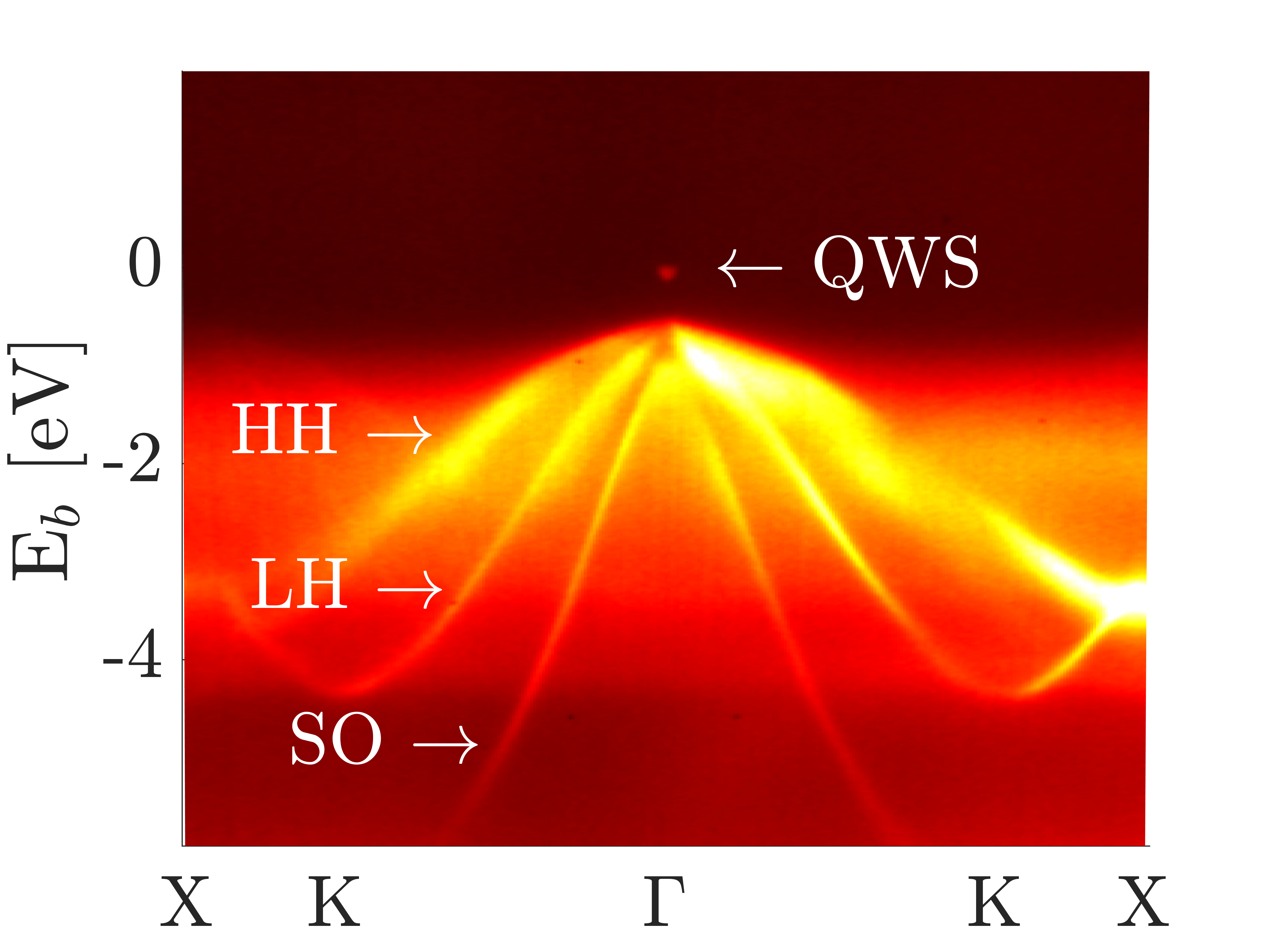
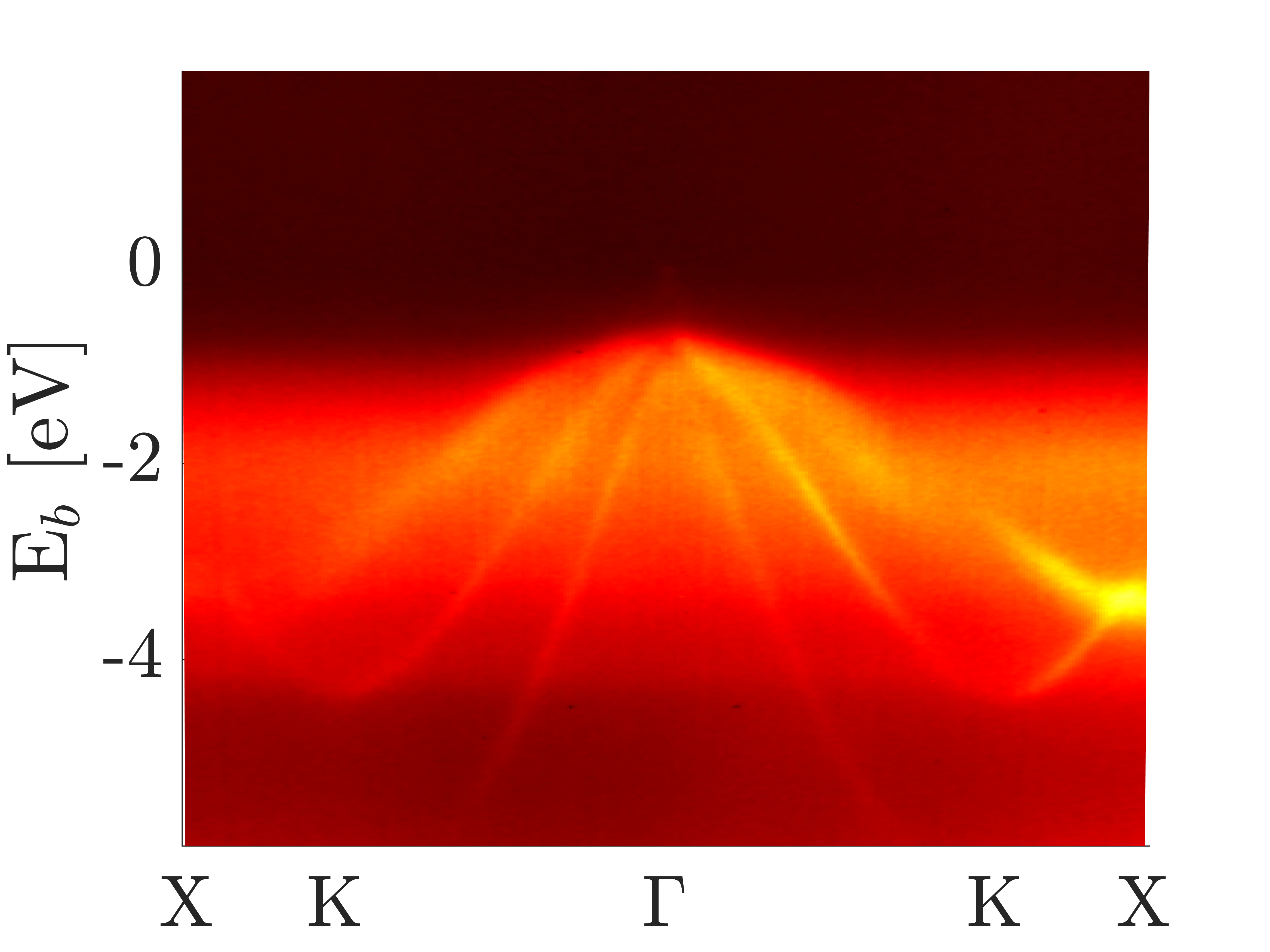
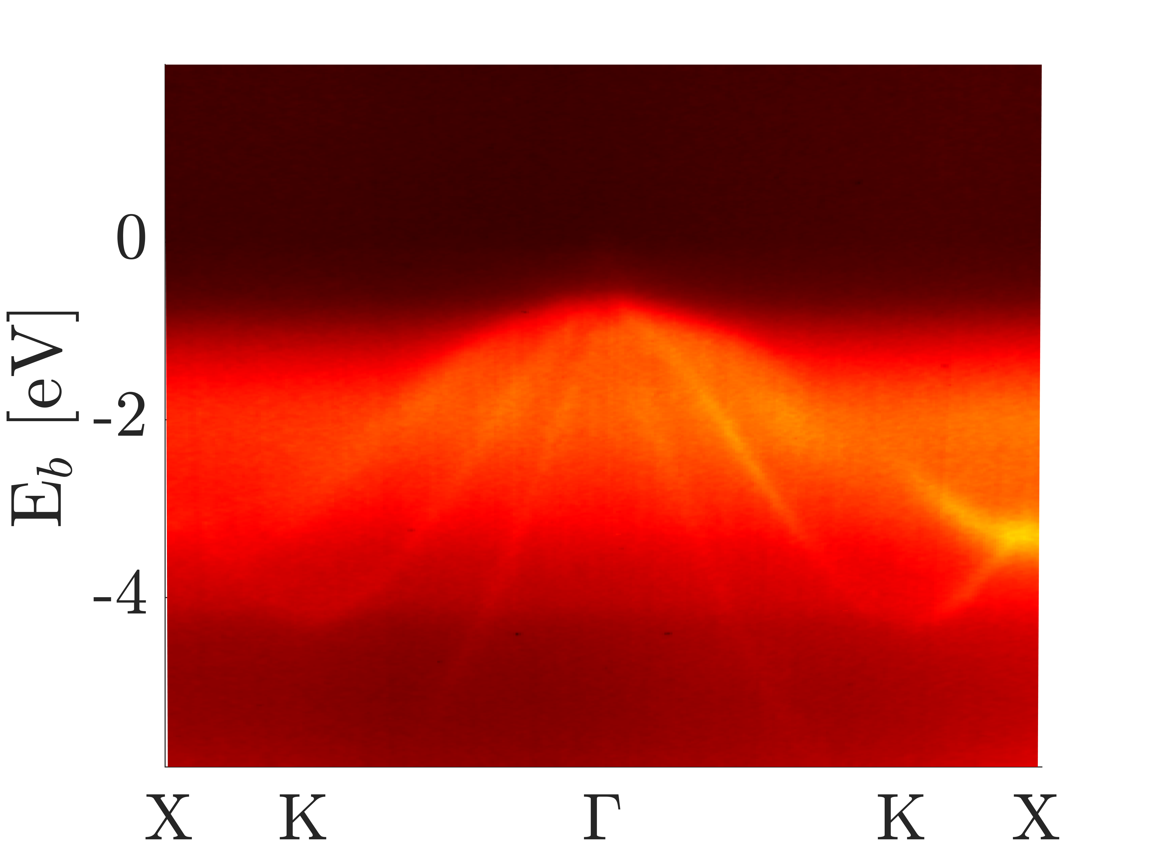
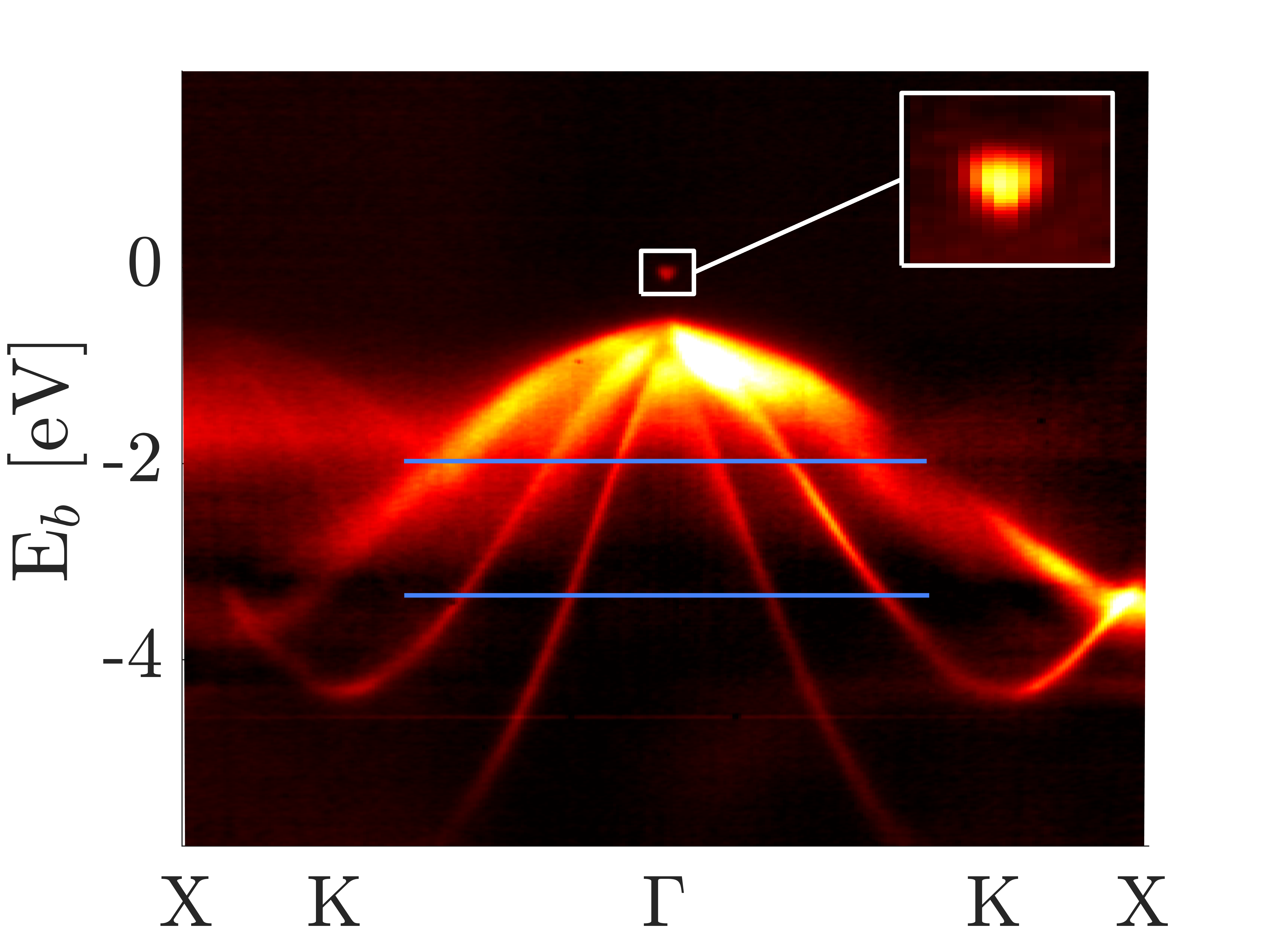
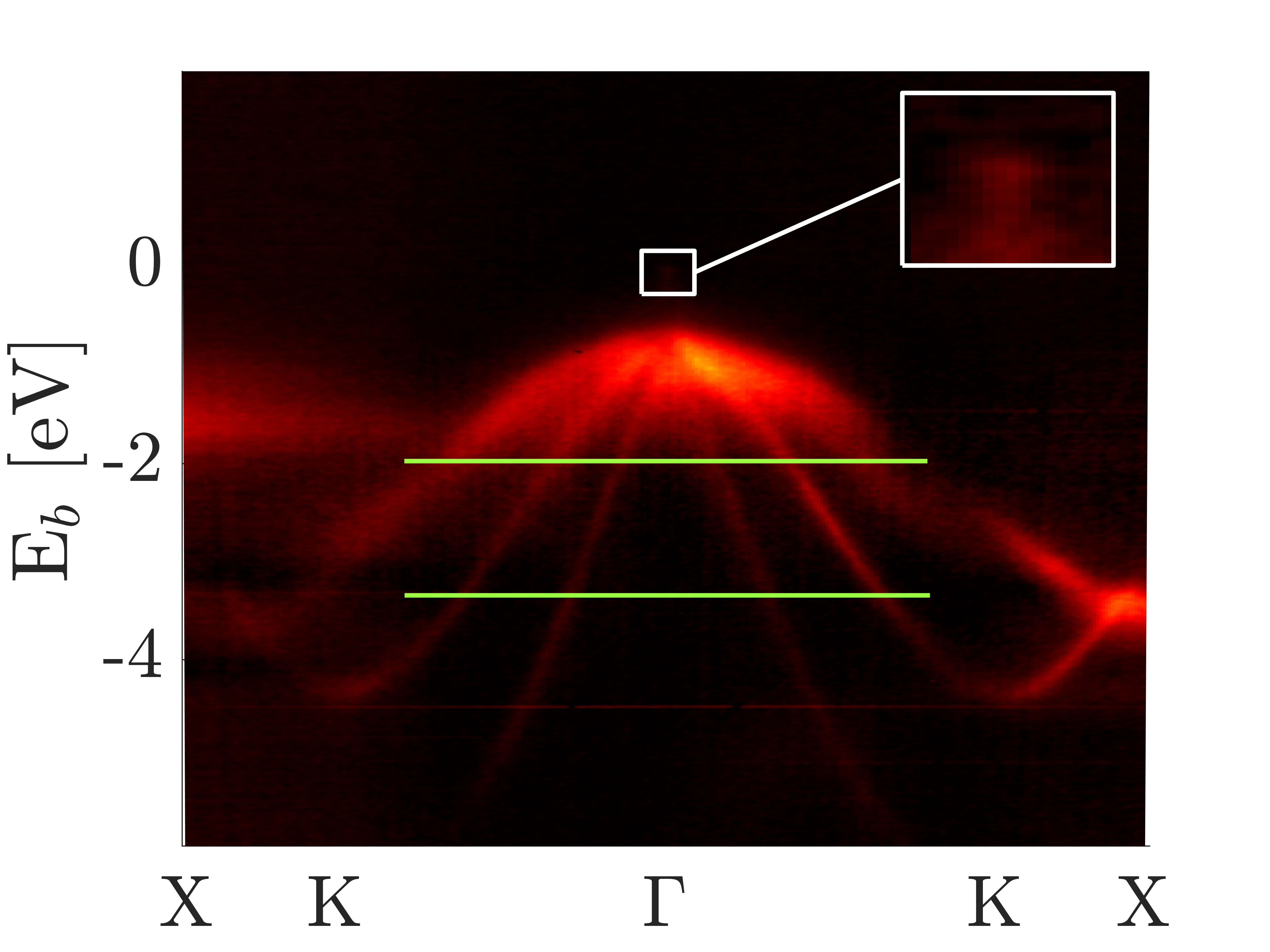
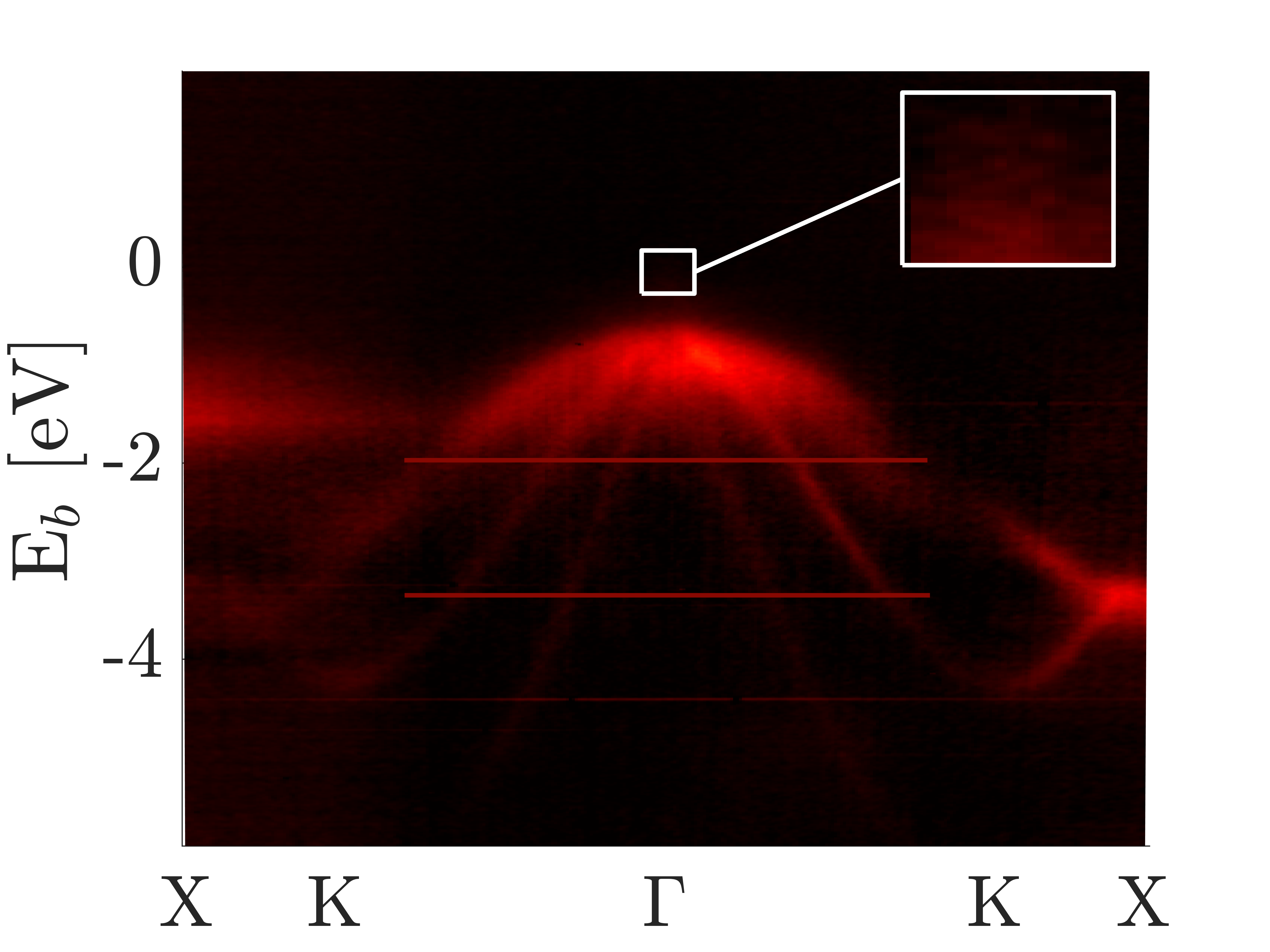
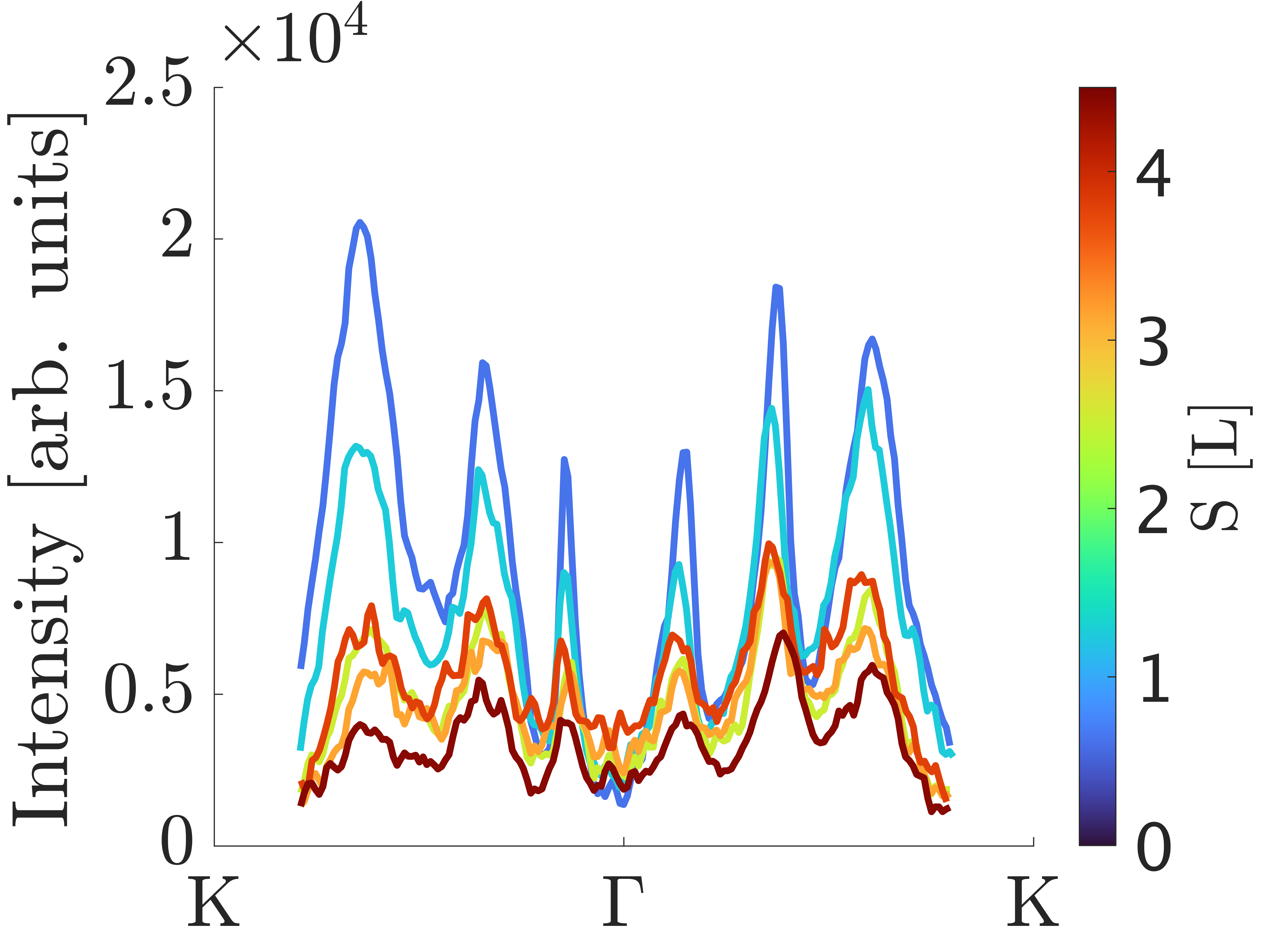
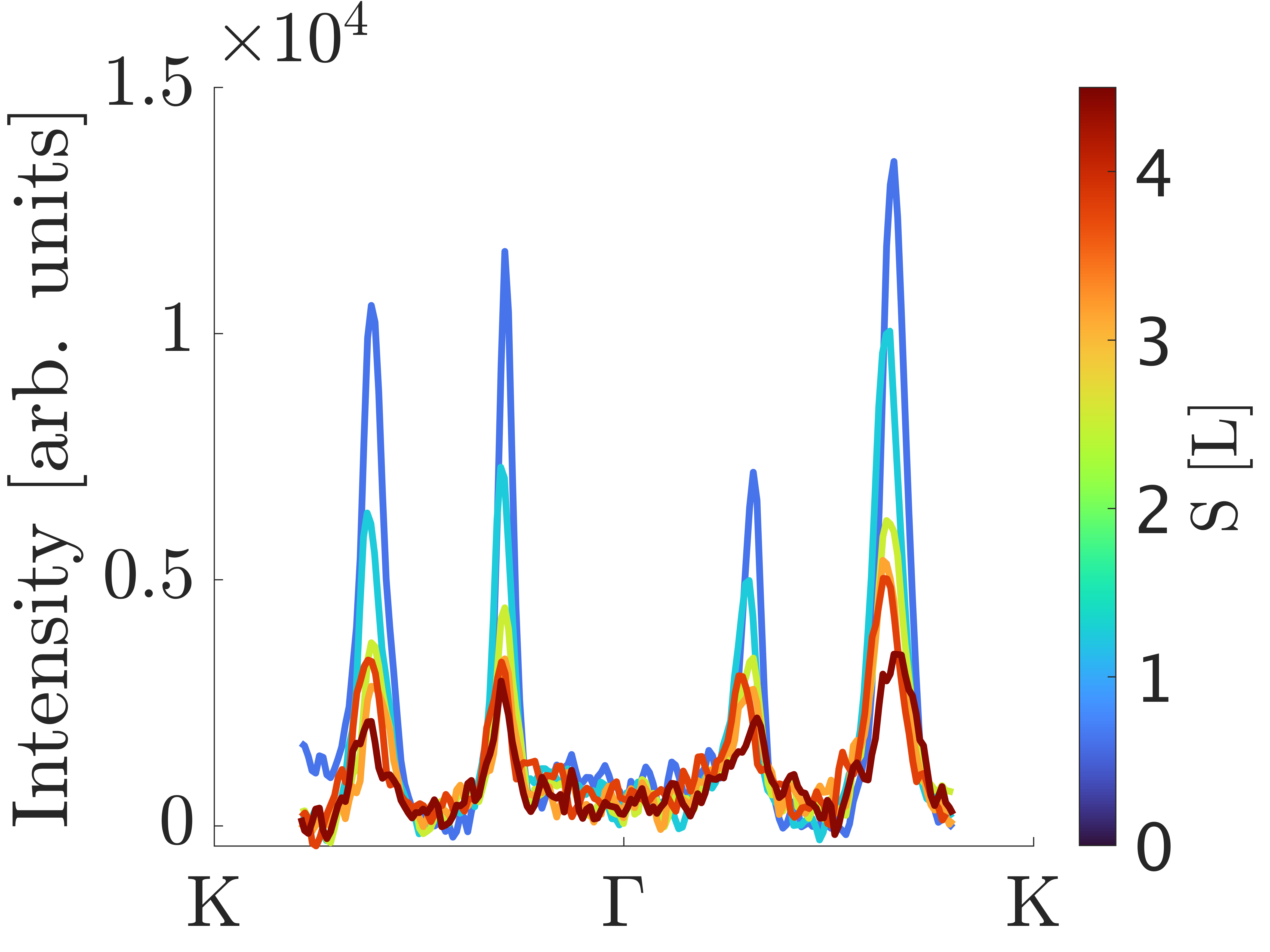
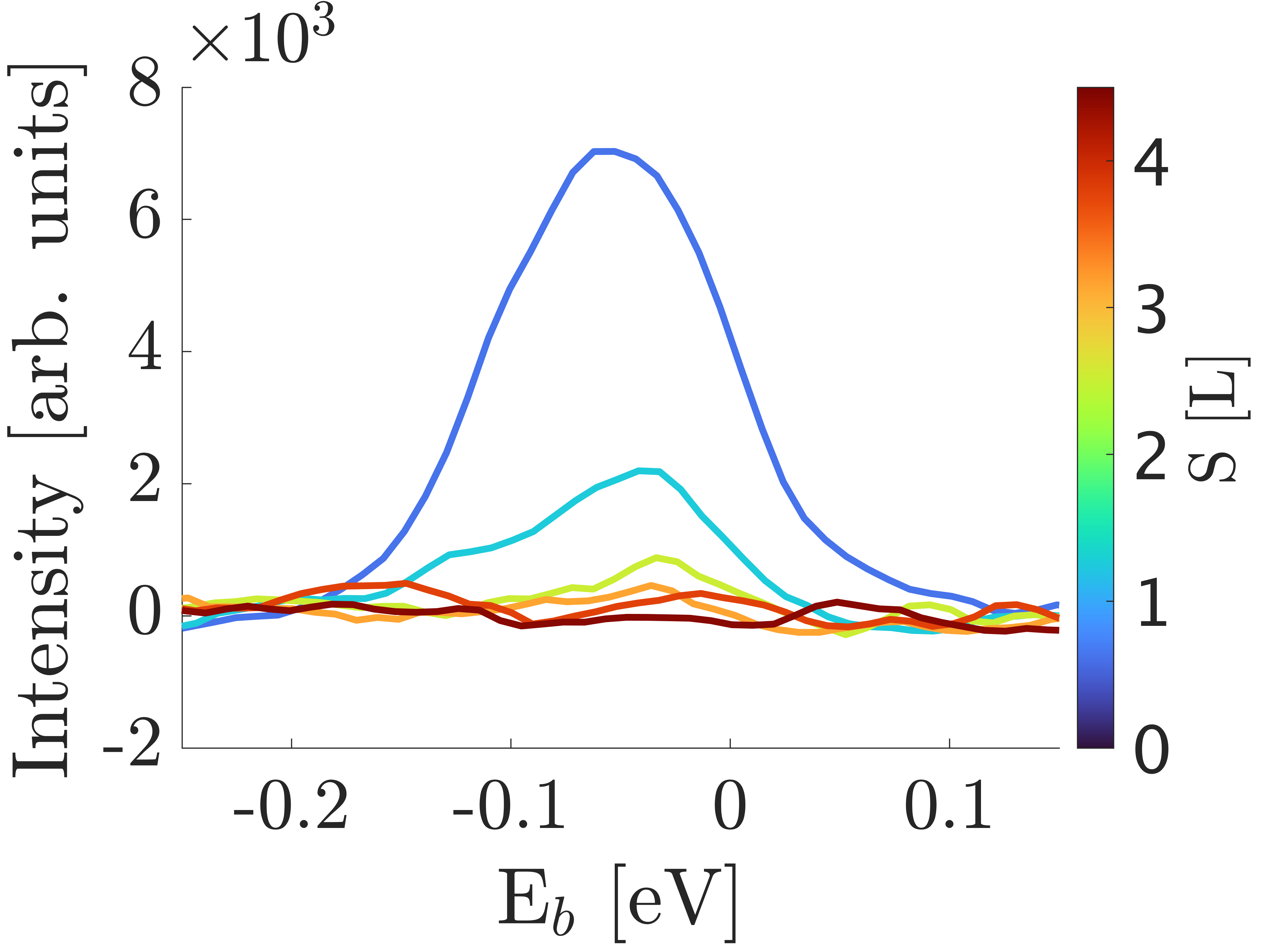
Fig. 1 presents the results of soft X-ray angle-resolved photoemission spectroscopy (SX-ARPES) measurements conducted along the KX high-symmetry line at , with varying sputtering doses. In Fig.1(a), we clearly identify the HH, LH, and SO valence bands. Figs. 1(a-c) show the ARPES data in ascending order of the sputtering dose, demonstrating that the coherent component of the valence bands remains robust against sputtering, as HH, LH, and SO can still be resolved in Fig. 1(c).
However, with increasing sputtering dose, the relative intensity of the coherent component decreases, and a momentum-independent density of states (DOS)-like intensity emerges across the entire Brillouin zone. The interplay between coherent and incoherent components depends critically on the degree of static disorder introduced by ion bombardment. We explain this phenomenon by introducing the coherence factor , as discussed in Sect. III.3.
In Figs. 1(d)-(f), we present the ARPES data after subtracting the incoherent intensity (see Appendix A). For the cleaved surface shown in Figs.1(a) and (d), we observe a pocket occupied by quantum well states (QWS) originating from the conduction band at the point. These states disperse just below the and approximately above the valence band maximum. We provide a blown-up image of this region, referred to as the CB region, in the upper right corner of Figs. 1(d)-(f). These QWS originate from charge accumulation in the vicinity of the native InAs(110) surface [26], and their presence confirms the pristine nature of the cleaved surface.
By examining the blown-up images of the CB region, we observe that, as the sputter dose increases, the coherent signal from the QWS depletes much faster compared to that of valence states. This qualitative difference in the response to disorder becomes even more pronounced when we compare the MDCs extracted from the valence band region in Figs. 1(g) and (h) with the energy distribution curves (EDCs) extracted from the CB region in Fig. 1(i). At approximately , the quasiparticle peaks of the valence states remain well pronounced, while the k-integrated spectrum of the CB region at shows no evidence of the presence of QWS. We argue that this phenomenon arises from the different scattering rates experienced by initial states close to the and well below it. If the electron-defect interaction is assumed to be quasi-elastic [27], the different scattering rates can be explained by the availability of defect-induced empty states to scatter into. For valence electrons, such states are occupied because of the sharp Fermi-Dirac distribution at and are unavailable for the quasi-elastic scattering. The conduction electrons near , however, have a large number of shallow defect-induced empty states at their disposal. This effect is similar to the electron-phonon scattering of the holes being active only within an energy interval around equal to the phonon energy, see, for example, Ref. [28].
III.2 Depth distribution of defects
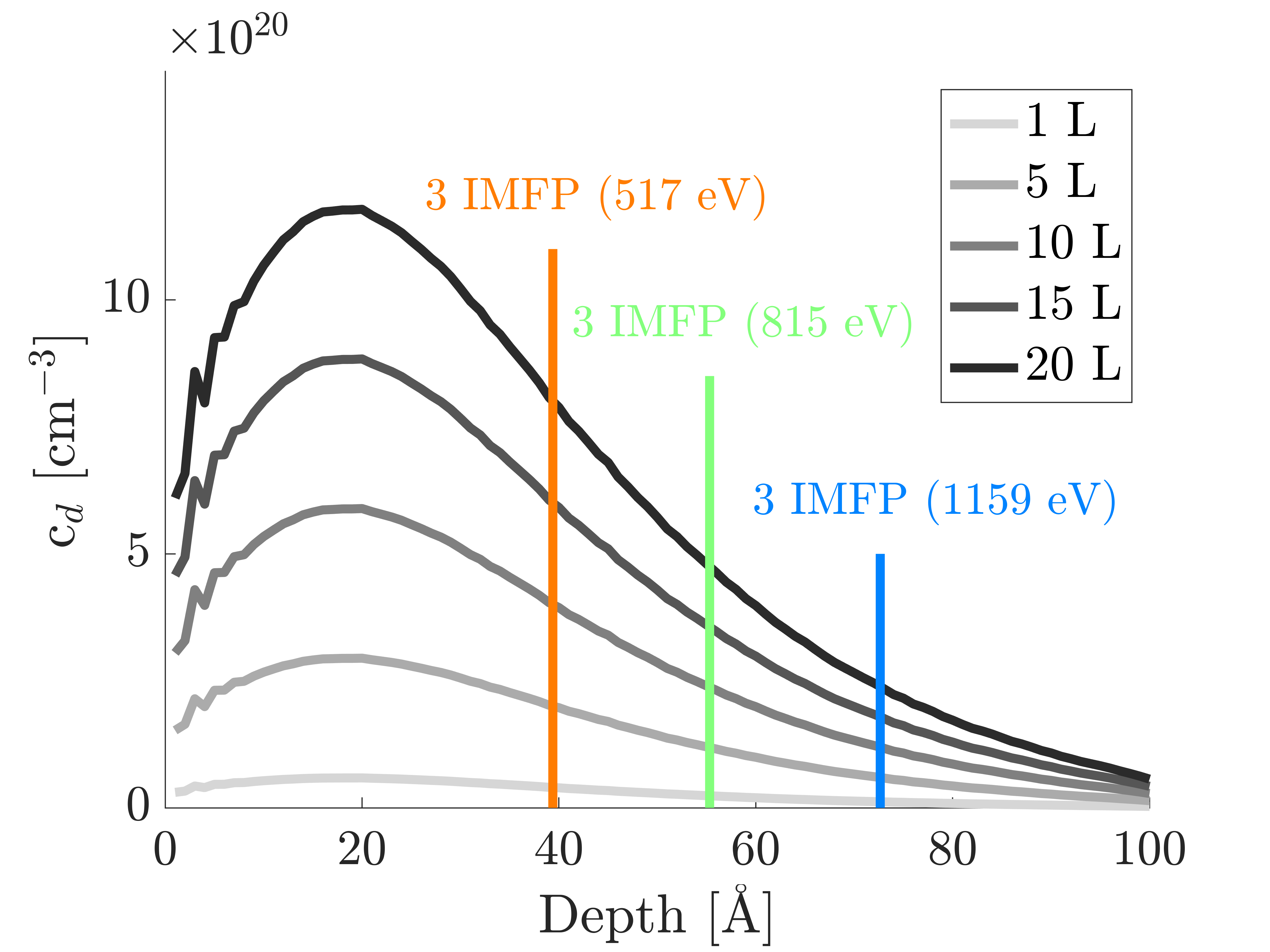
Fig. 2 (a) shows the total concentration of vacant In and As sites calculated using SRIM [29]. Each of these displaced atoms stops at some interstitial site, effectively creating a second defect. For comparison purposes, the probing depth in the pristine sample, namely 3 times the IMFP [1], is plotted on top of the defect distribution.
Since, according to [30], the energy to displace an In atom is slightly smaller compared to that of As, the In atoms are displaced more frequently during the bombardment process. Furthermore, the peak position at is explained by the cascade effect, generated by the Ar ions that displace target atoms, which in turn create more defects as they propagate away from the surface.
We point out that the simulation does not include temperature effects, which lead to self-annealing processes and therefore to a general reduction of the defects’ concentration. Further, the simulation does not take into account the fact that atoms sitting at damaged areas of the crystal need less energy to be displaced. This leads to an underestimate of the actual concentration of defects.
III.3 The coherence factor
Here, we show how the sputter-induced disorder can effectively be explained by an extended version of the DWF. Originally, this theory was developed to describe the effects of temperature on photoemission spectra. At finite temperatures, the atoms that constitute the crystal vibrate around their ideal lattice positions. The fact that during the photoexcitation process the atoms are not localized at their perfect lattice sites creates a phase mismatch between the initial and final states. This has severe consequences for the total coherent intensity . In fact, depending on either the temperature or photoelectron kinetic energy, the mismatch between the initial and final states can gain importance and eventually deplete a large portion of the coherent intensity. This depletion can be quantified via the DWF, W, which is normally interpreted as the fraction of coherent intensity that reaches the detector [31, 32]:
| (1) |
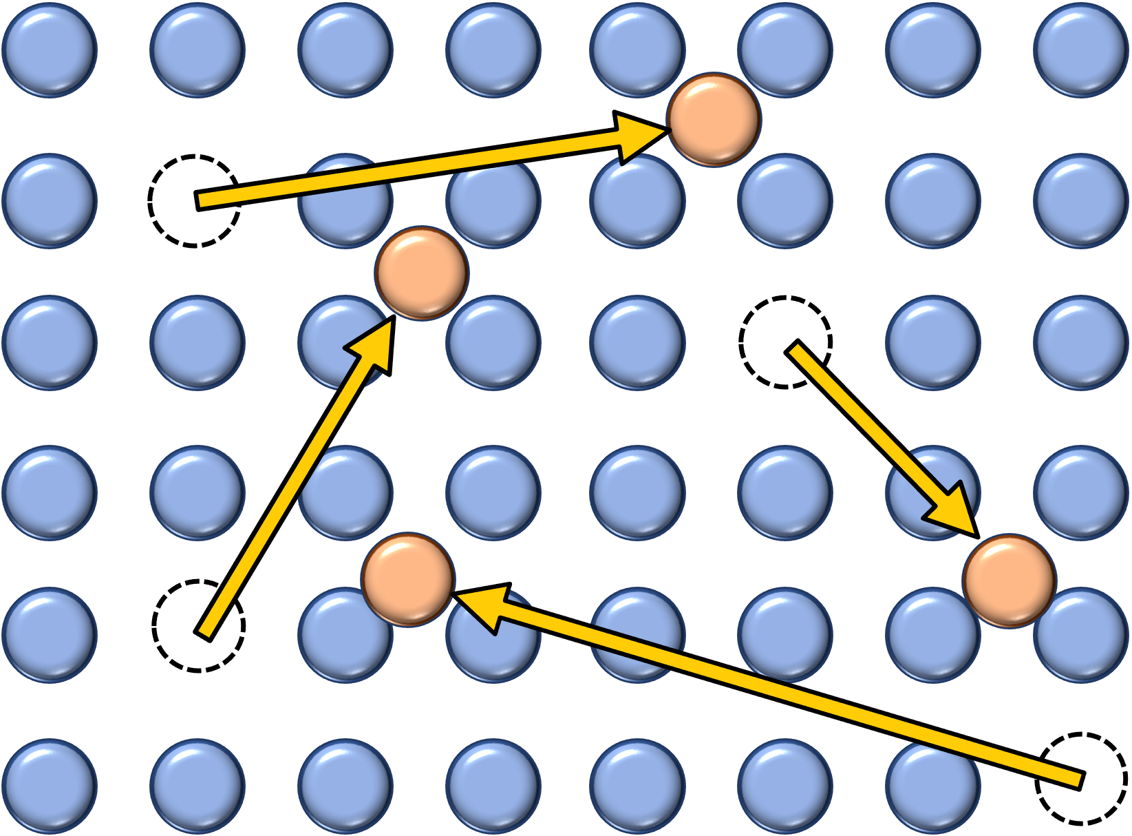
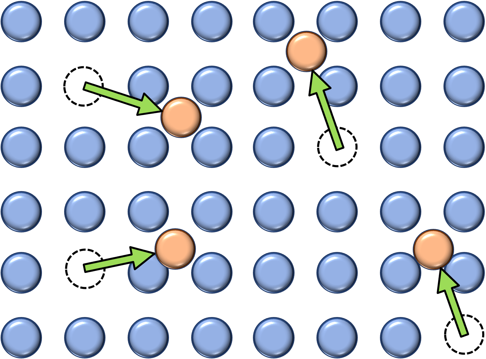
In Eq. 1, is the reciprocal lattice vector that connects the reduced and actual wave vector of the final state and is the average square displacement of the atoms, due to thermal vibrations. The former quantity strongly depends on the photoelectron kinetic energy and, in turn, the photon energy . In particular, the higher , the more important the phase mismatch becomes and, consequently, the smaller the portion of the coherent intensity. In the usual Debye-Waller picture, is proportional to temperature. In this paper, we extend the DWF to the case of static disorder. This step is also motivated by the successful treatment of thermal fluctuations within the one-step model [33], more precisely using the Coherent Potential Approximation (CPA) [34] within the multiple scattering theory or the KKR formalism. Here, the thermal fluctuations of the atoms are approximated by a finite number of static displacement vectors. Furthermore, the sum of the squares of these vectors, weighted with the probability of such a displacement, is forced to be equal to [35]. Therefore, to describe the effects of static disorder on the ARPES spectral intensity, caused by collision cascades of incident ions that generate vacancies and interstitials (as shown by the yellow arrows in Fig. 3(a)), we propose an averaged square displacement, , which depends on the concentration of defects . To do so, we introduce the concept of an “effective displacement”, which is illustrated by the green arrows in Fig. 3(b). Here, it shows that the actual displacement of the atoms is not important; rather, only the average minimal distance between the vacancies and interstitials is important to determine .
To estimate , we first make a few assumptions about the distribution and nature of the vacancies and interstitials. First, we only consider the case where the vacancies and interstitials are statistically distributed within the sample. This means that the concentration of defects (i.e., vacant and interstitial atoms) is homogeneous throughout the sample and is entirely equivalent to the case of a perfectly thermalized sample under the standard DW formalism. At this point, we consider the volume , which on average contains exactly a vacant lattice site and an interstitial. The average distance between these two defects is given by , where is a constant that depends on the geometry of the problem. Next, we neglect the contribution from atoms displaced from their lattice sites by the attractive (repulsive) force exerted by some vacant (interstitial) atom. Finally, we get , where is the total number of atoms in the crystal, is the number of defects (either vacant or interstitial atoms) and is the volume occupied by a single atom. Therefore, by replacing with our new definition of in Eq. 1, we define the coherence factor as:
| (2) |
We therefore propose that Eq. 2 can be used to estimate the fraction of coherent intensity that originates from the static and homogeneous disorder within a crystalline sample. To some extent, is equivalent to the DWF, where plays the role of an effective temperature.
Moreover, the contributions of static and thermal disorder to the total mean displacement can be approximated according to . Notice that this is only possible if the thermal and static displacements are completely unrelated, only then can we assume a vanishing cross-term . As a result, the total portion of coherent intensity is given by the product of and W, namely . Finally, we can make use of the DW theory to decompose the total ARPES spectral intensity as [31, 32, 36, 37]:
| (3) |
where is the momentum-dependent coherent component that originates from Bloch electrons in the unperturbed crystal structure, is the incoherent component associated with final states that scatter at least once with the defect potential, and is the remaining background of photoelectrons scattered by electron-electron interaction.
III.4 Depletion of coherent intensity
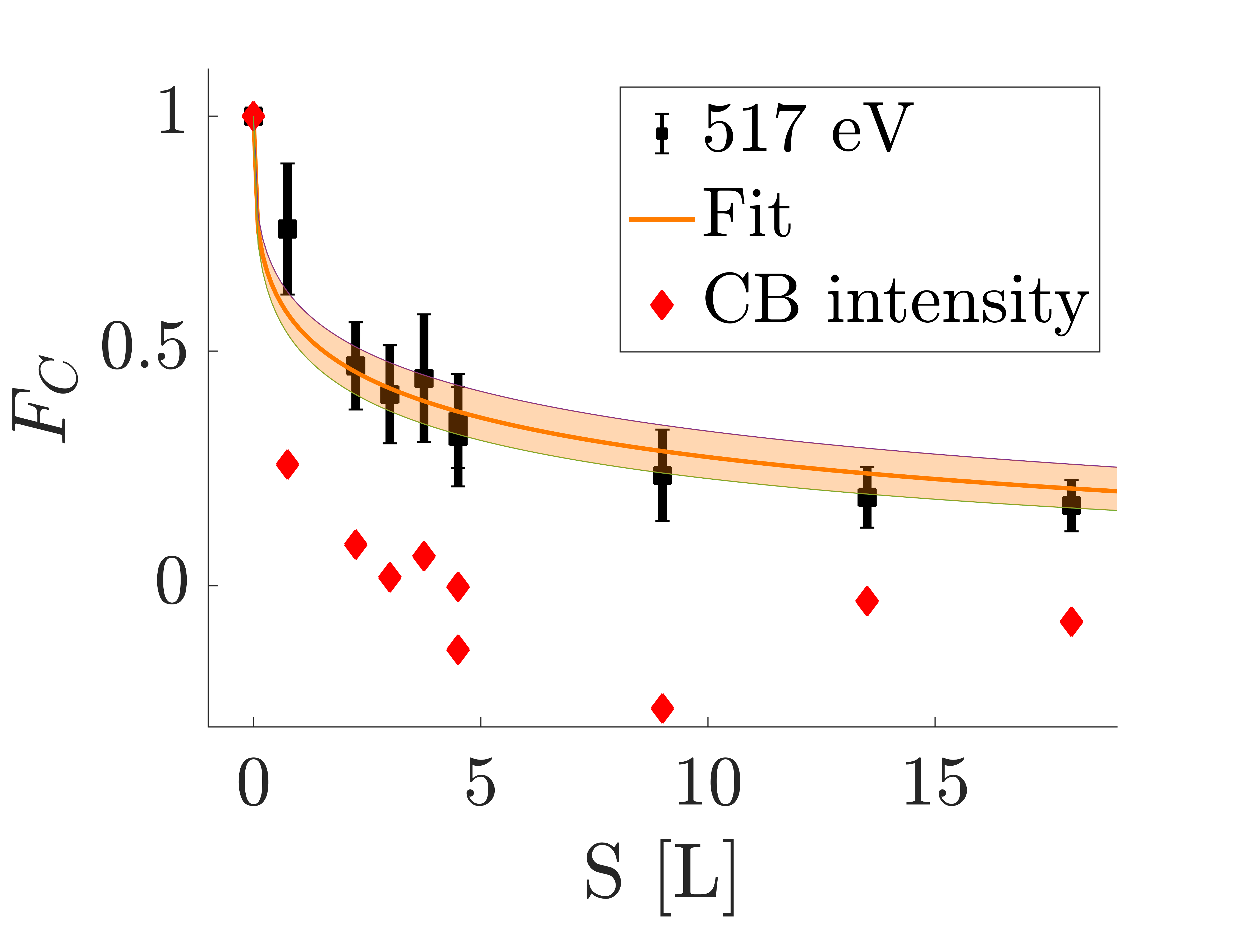
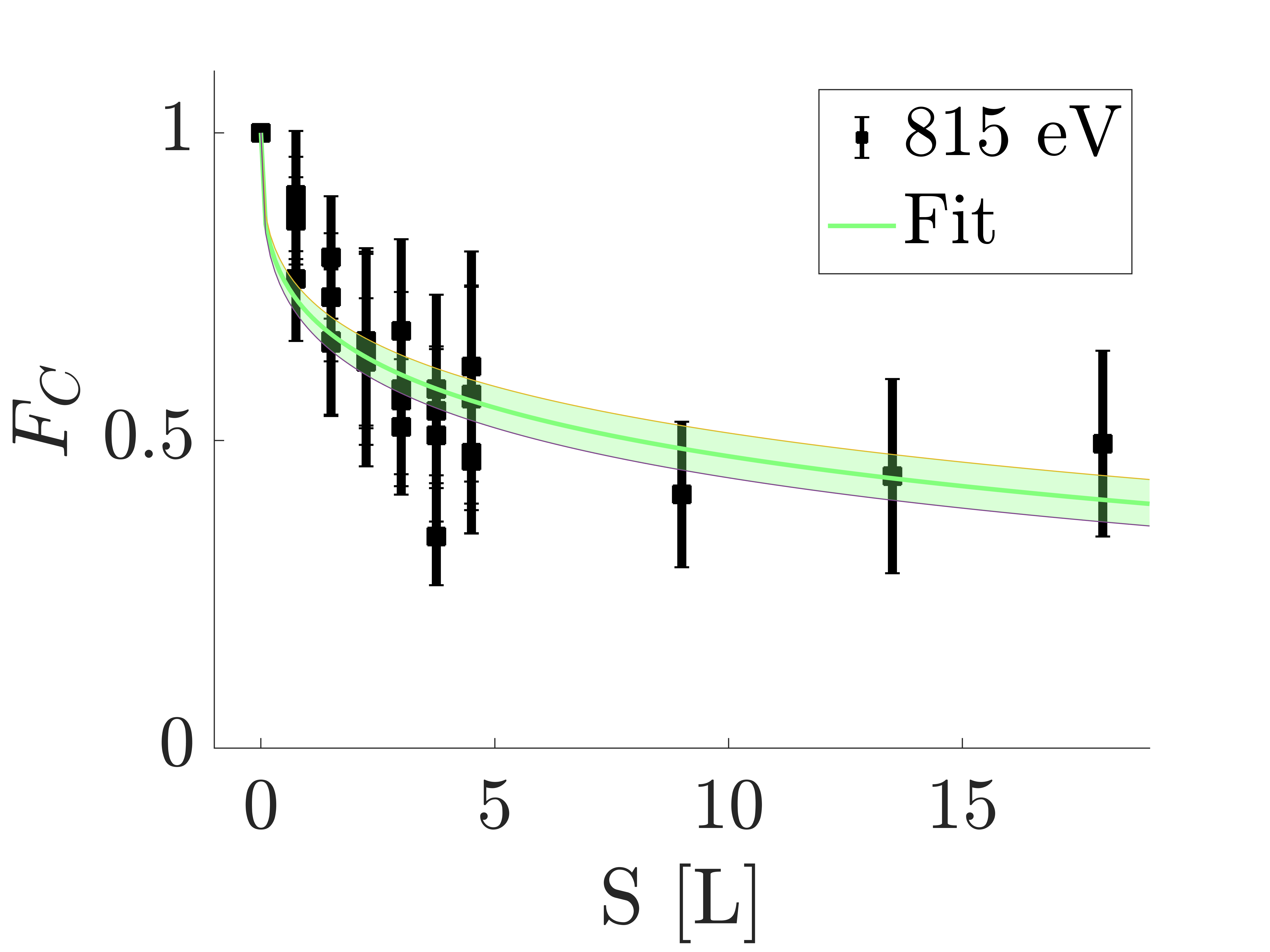
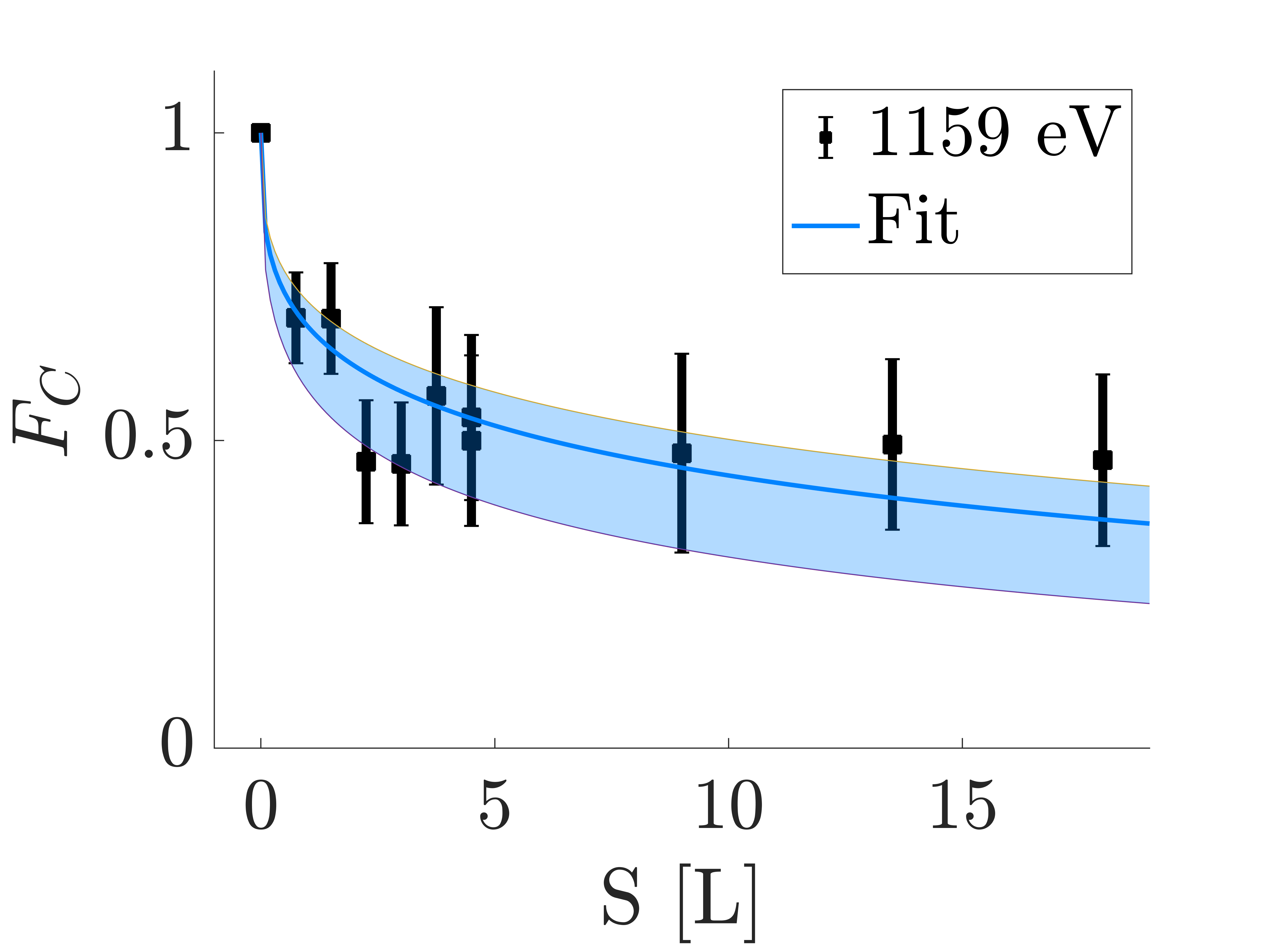
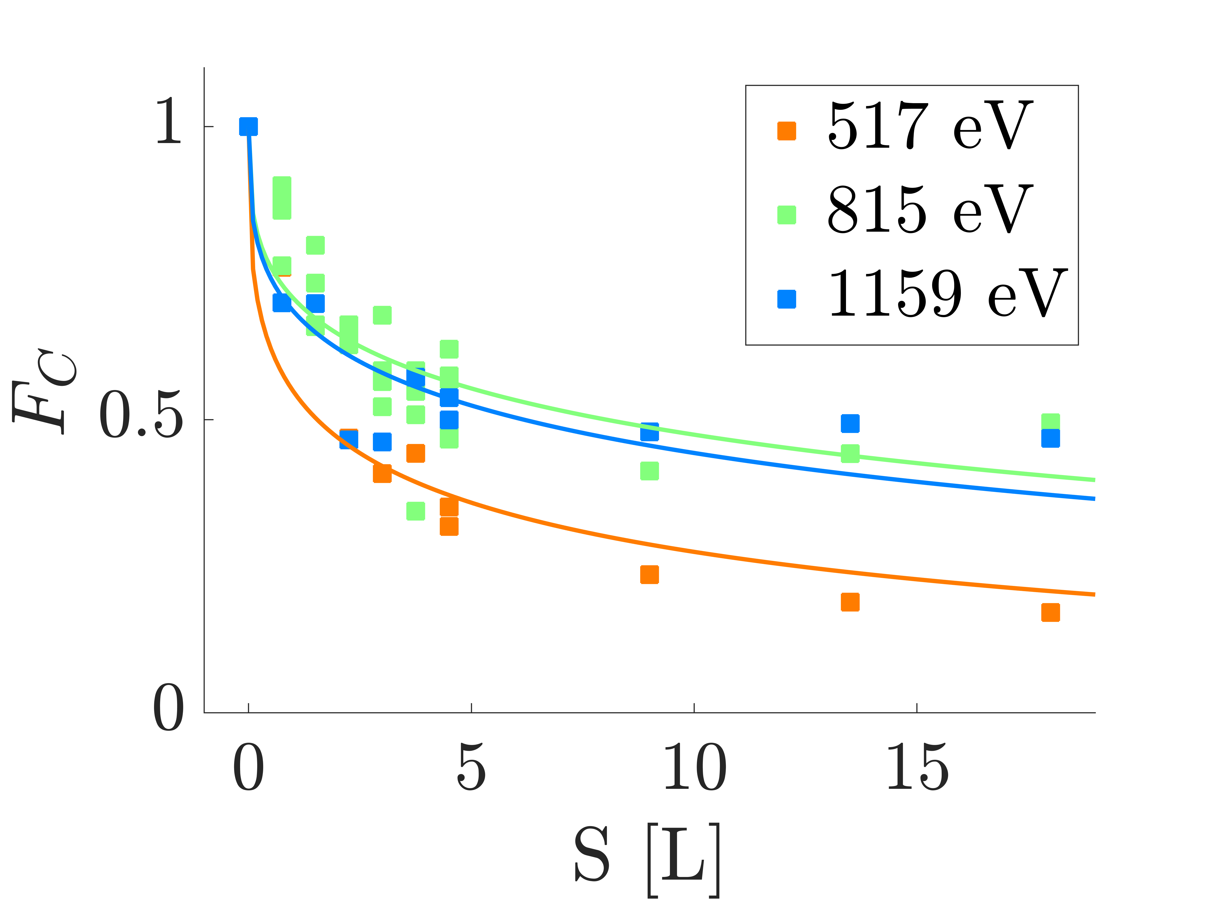
The is obtained by the fitting procedure explained in Sect. II and Appendix B. This method gives us direct access to the relation versus the sputtering dose , which is shown in Fig. 4, for the different photon energies. Next, to fit the dependence of on , we assumed an average defect concentration, which is related to the sputtering dose through the linear relation . We refer to as the concentration rate constant. Let us insert this into Eq. 2, and obtain the fitting function
| (4) |
effectively ignoring thermal effects. Quantities and are known [38], while the parameter is optimized to fit the experimental results. The optimal values for are contained in Tab. 1, in Appendix C. These results show that . This implies that the effective defect concentration is higher for photoelectrons with lower energy. This is easily explained by the simulated defect distribution in Fig. 2 (a). This figure shows that, on average, the electrons excited with , are localized in the sample slab with the highest concentration of defects. Generally the IMFP of the final states increases with [39, 40], and as a result, the probed sample slab has a lower average . This phenomenon is reflected in the higher defect rate constant , which converts the sputtering dose into an effective concentration. Unfortunately, we only have access to , and, as mentioned above, is unknown. But since the latter is not expected to change as a function of , we can divide two different values and obtain the ratios between the corresponding defect rate constants. The results of this procedure are , and . These quantities are in good agreement with the averaged concentration rate constants , obtained with the SRIM simulation, although the large uncertainties prevent a meaningful quantitative comparison.
Lastly, we discuss the intensity of the CB region measured at , as shown in Fig. 4(a), as a function of . To obtain these data points, we integrated the intensity over the momentum coordinate, subtracted the quadratic background, integrated over the energy coordinate, and subsequently normalized the results. By comparing these data points with , we confirm the faster decay of the QWS intensity in contrast to the valence states observed in Sect. III.1.
III.5 Spectral broadening
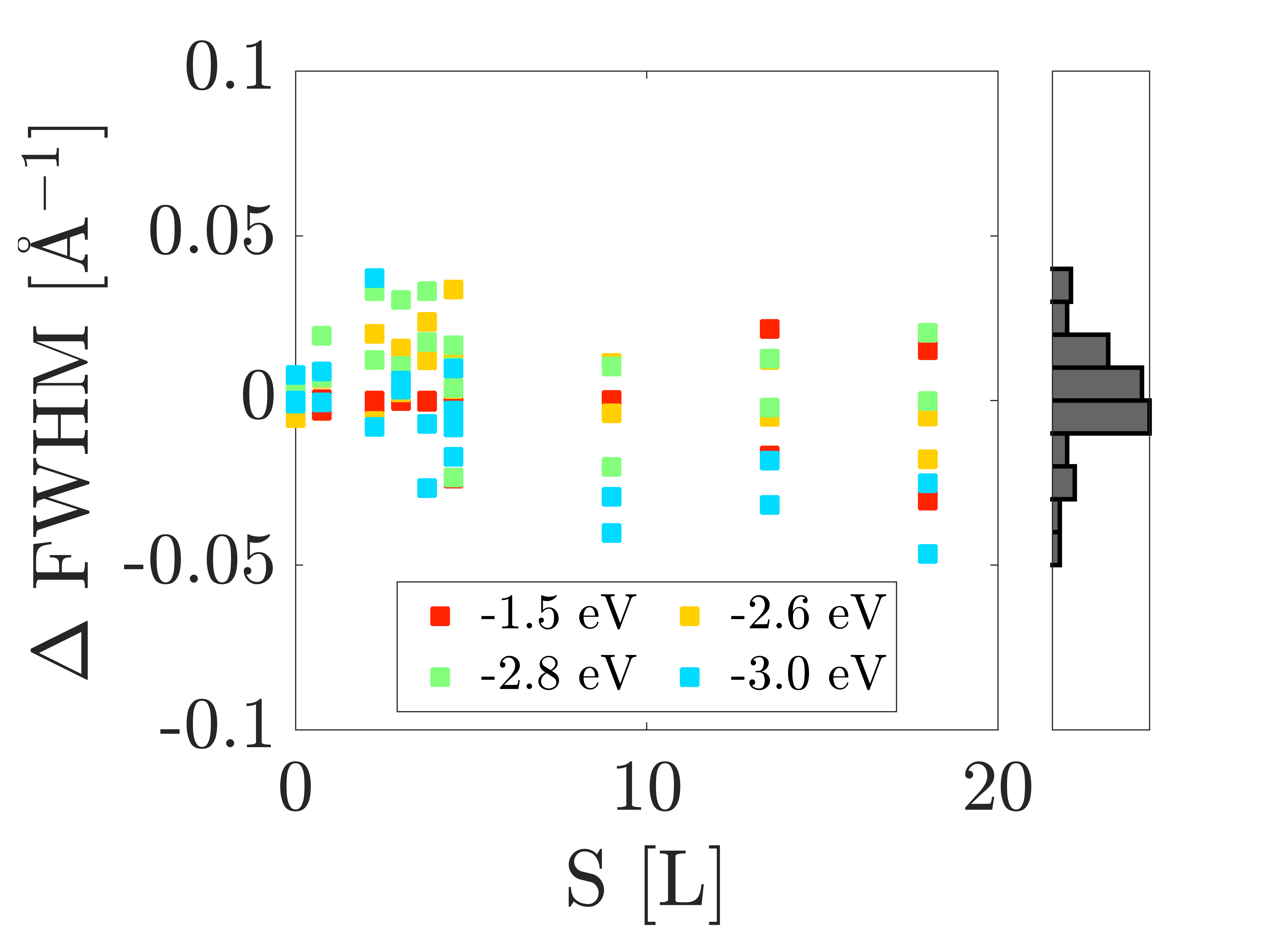
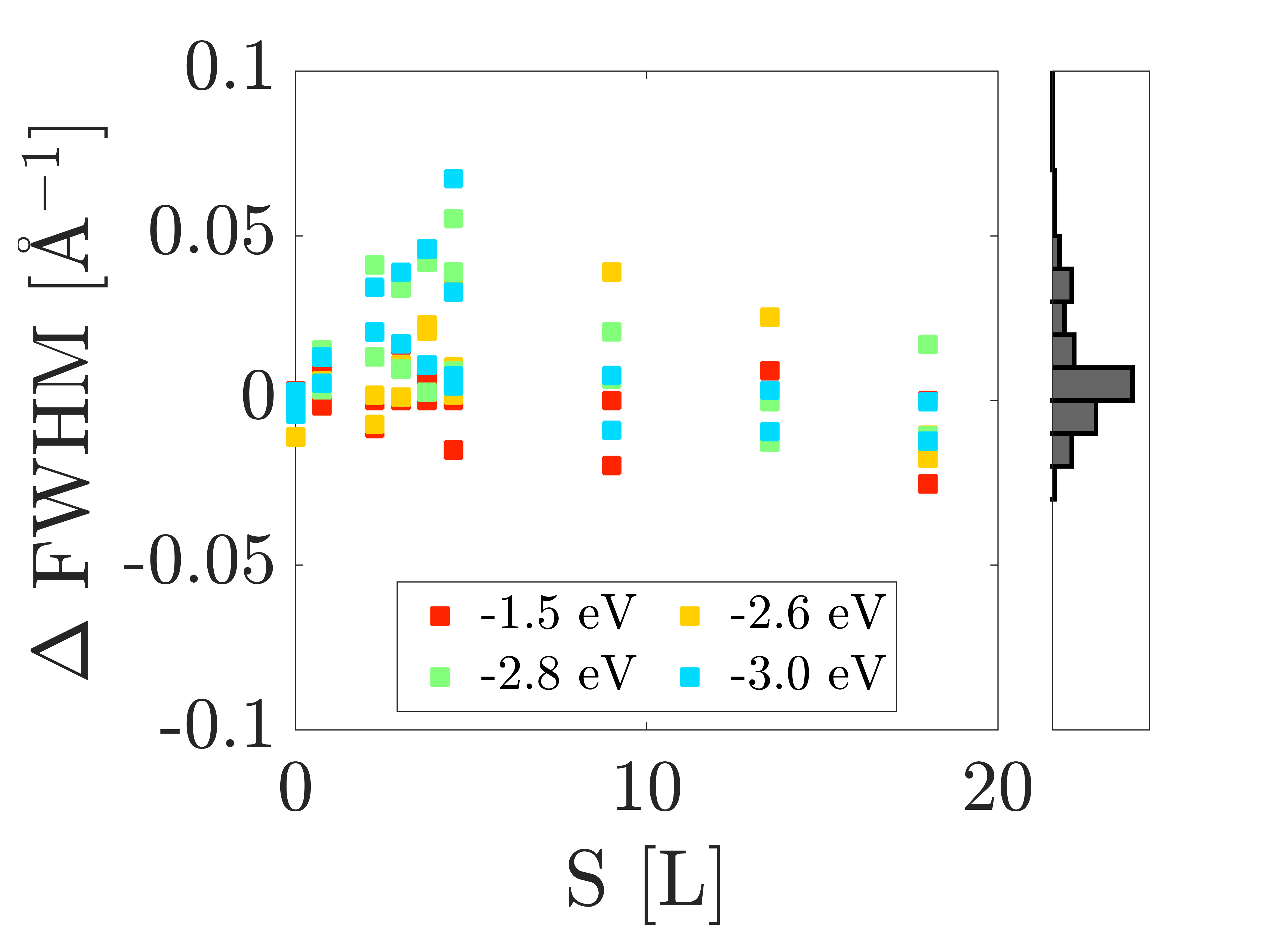
We measured the widths of the MDC peaks of the split-off (SO) and light hole (LH) bands along KX as a function of . Specifically, we focused on the data set for the analysis. This choice is justified by the higher reliability of MDC fitting at lower photon energies, where the coherent intensity contributes more significantly to the overall signal, and the energy resolution is higher. Figs. 4(e) and (f) depict as a function of , obtained using the method explained in the previous section. Here, and represent the FWHM obtained by fitting the MDC and EDC peaks, respectively. We highlight the linear relation between the FWHM along momentum and energy, which is given by , where denotes the band velocity.
At , the results for both SO and LH bands indicate that the linewidths are constant as a function of . As the right panels of Figs. 4(e) and (f) show, the data points are distributed around zero, with a spread of approximately . For reference, at , the energy resolution is approximately , which corresponds to along the momentum direction when weighted by the inverse velocity of the bands within the region of interest.
Generally, the presence of defects is expected to decrease the lifetime, thereby reducing the elastic mean free path of the initial and final states [41]. These effects contribute to an increase in the widths of the spectral lines along the energy direction [42]. The absence of broadening in the valence bands aligns with the slower depletion of coherent intensity, relative to the QWS, observed in the previous sections. This observation supports the theory that defect scattering is mainly quasi-elastic, and the absence of empty states below prevents scattering of the initial valence states, effectively ensuring conservation of momentum.
IV Conclusions
In conclusion, we extended the use of the DWF, originally applied to describe thermal disorder, to account for static disorder in ARPES measurements. The coherence factor, denoted as , serves as the analogue of the DWF for static disorder. We also showed that , in conjunction with the DWF, allows considerations of thermal and static disorder effects on the same footing. Our experimental results obtained on ion-bombarded InAs(110) exhibit excellent agreement with , thereby reinforcing its applicability in explaining the depletion of coherent intensity in the valence bands.
Furthermore, our investigation unveils a notable difference in the depletion rates of ARPES intensity between conduction electrons, in form of quantum well states, and valence electrons in InAs(110) subjected to ion bombardment. This dissimilarity arises from the predominance of quasi-elastic defect scattering. The availability of phase space for scattering varies between initial states at and valence states. Conduction electrons possess a large number of states suitable for quasi-elastic scattering, whereas valence electrons lack empty states below . Consequently, in the presence of defects, conduction electrons experience higher scattering rates compared to valence electrons.
Moreover, our measurements of the linewidths of the valence band peaks, demonstrate no momentum broadening as a function of sputtering dose within our resolution limit of . These findings support our hypothesis that the electron-defect interaction predominantly involves quasi-elastic scattering. As a result, valence initial states are unable to undergo scattering events that would shorten their lifetime, effectively preventing lifetime broadening of the bands.
Overall, our observations shed light on the unique depletion characteristics of ARPES intensity in ion-bombarded InAs(110) and provide insights into the quasi-elastic nature of defect scattering and its impact on electronic states.
Appendix A Separation of coherent and incoherent intensity
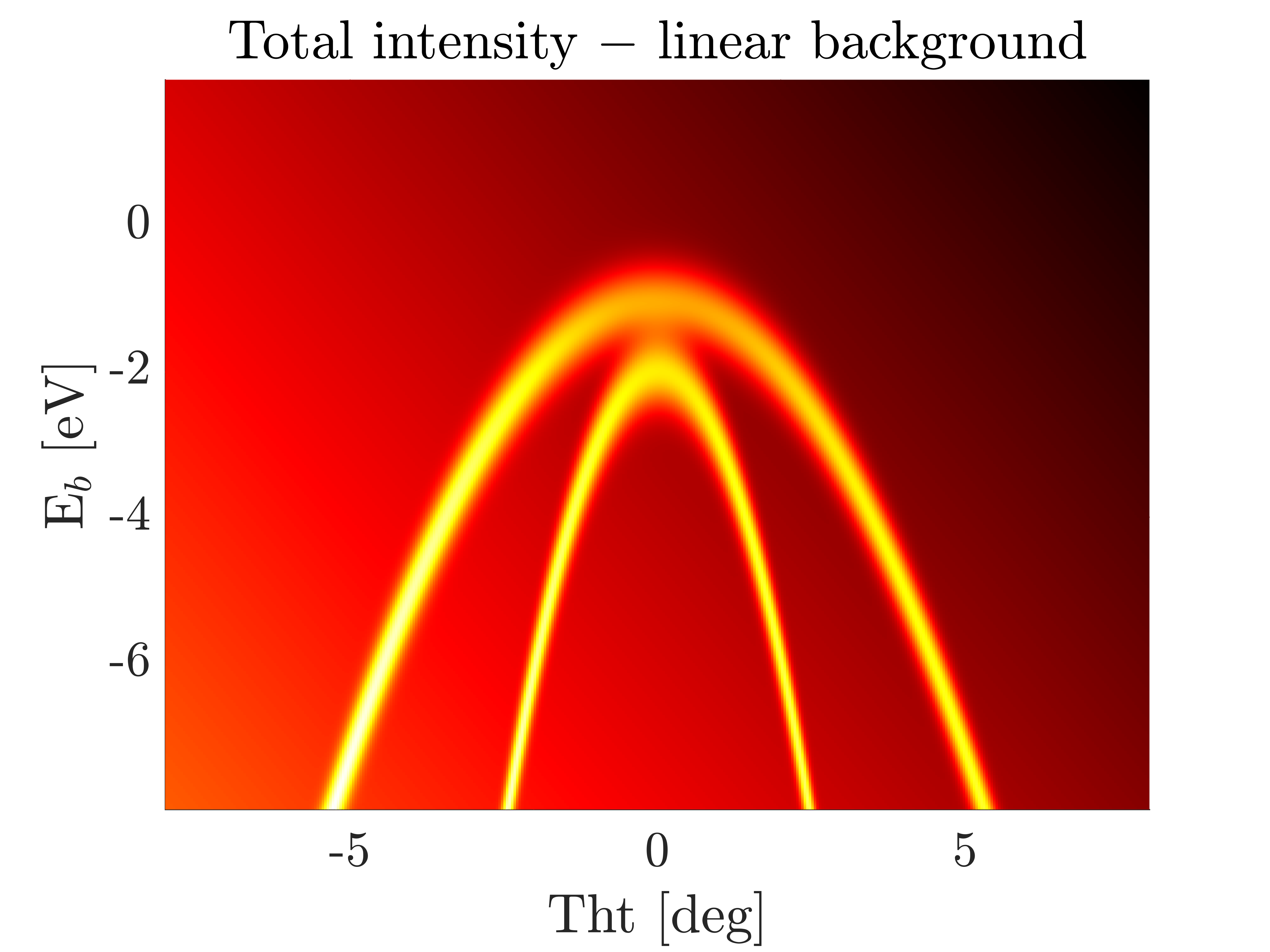
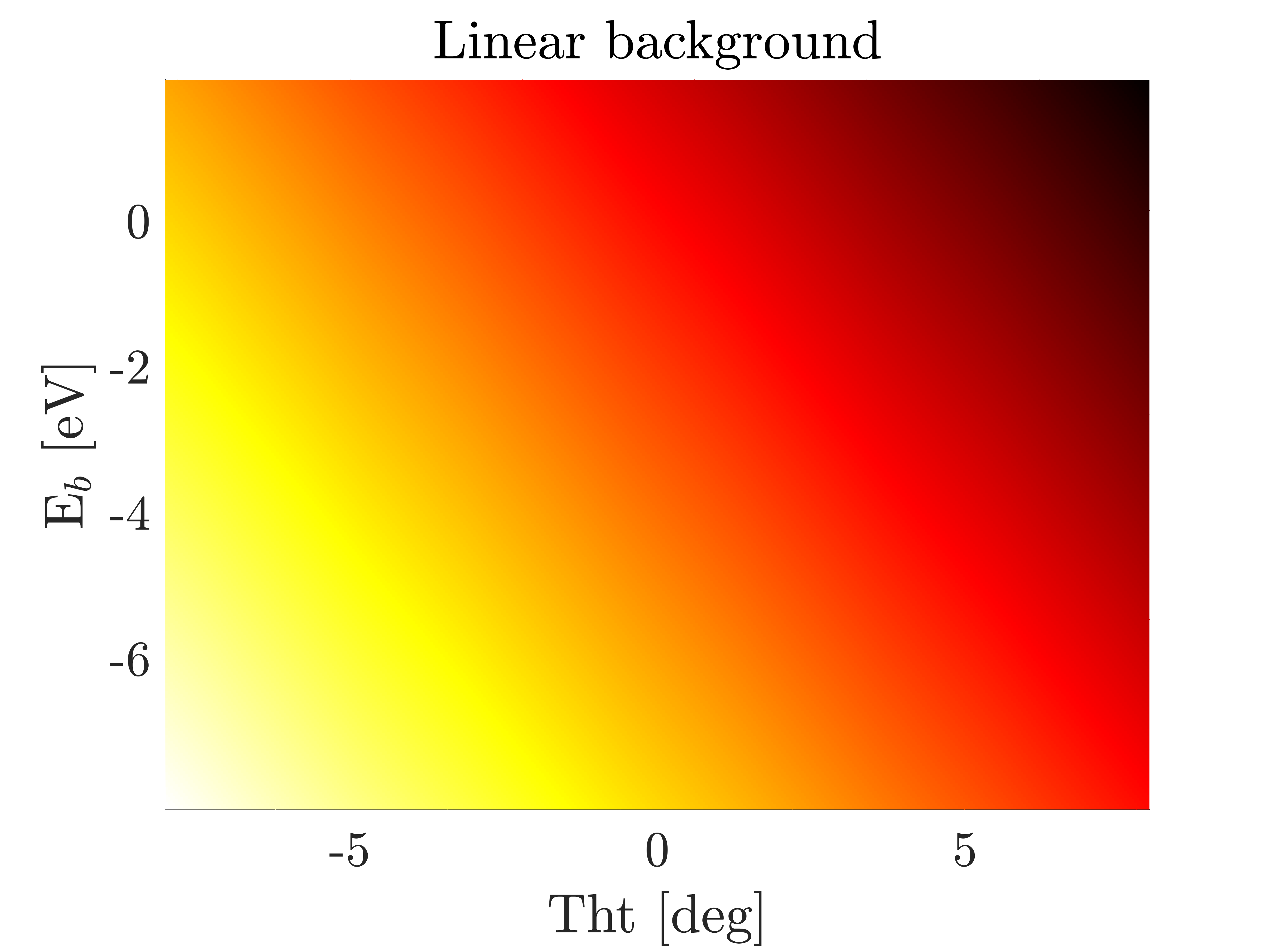
To extract the coherent fraction of the intensity from the measured ARPES spectra, we implemented an algorithm in MATLAB. This function divides the ARPES data into MDCs. The first step was to convolve the MDCs extracted from the total intensity with a Gaussian to smear out the coherent peaks. Next, we defined the first approximation of the background as the minimum between the total intensity and its convoluted counterpart. The final background was obtained after several iterations of this step. In particular, at every step, the total intensity was replaced by the background obtained in the previous iteration. To obtain the coherent intensity, we subtracted the background from the total intensity.
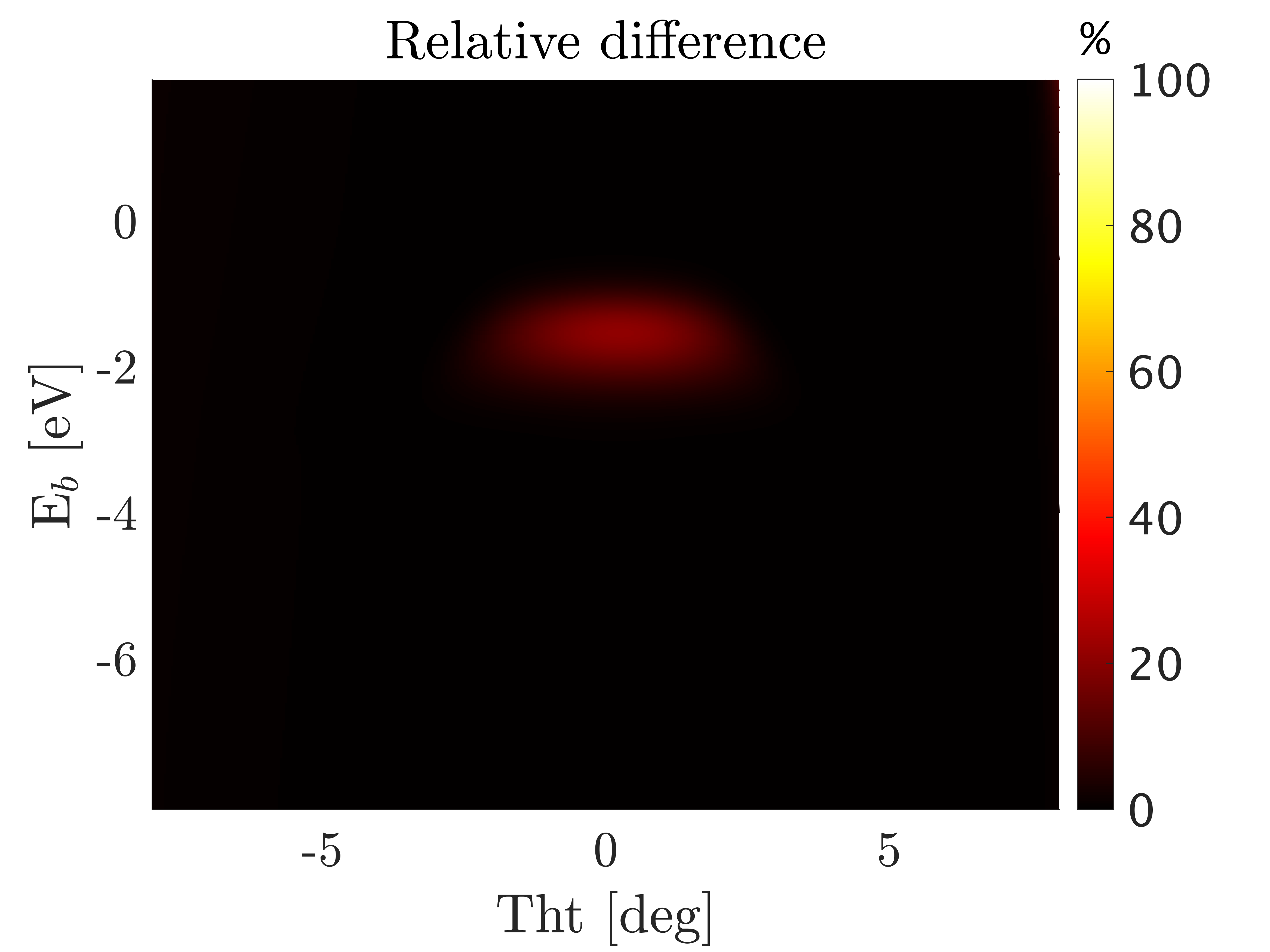
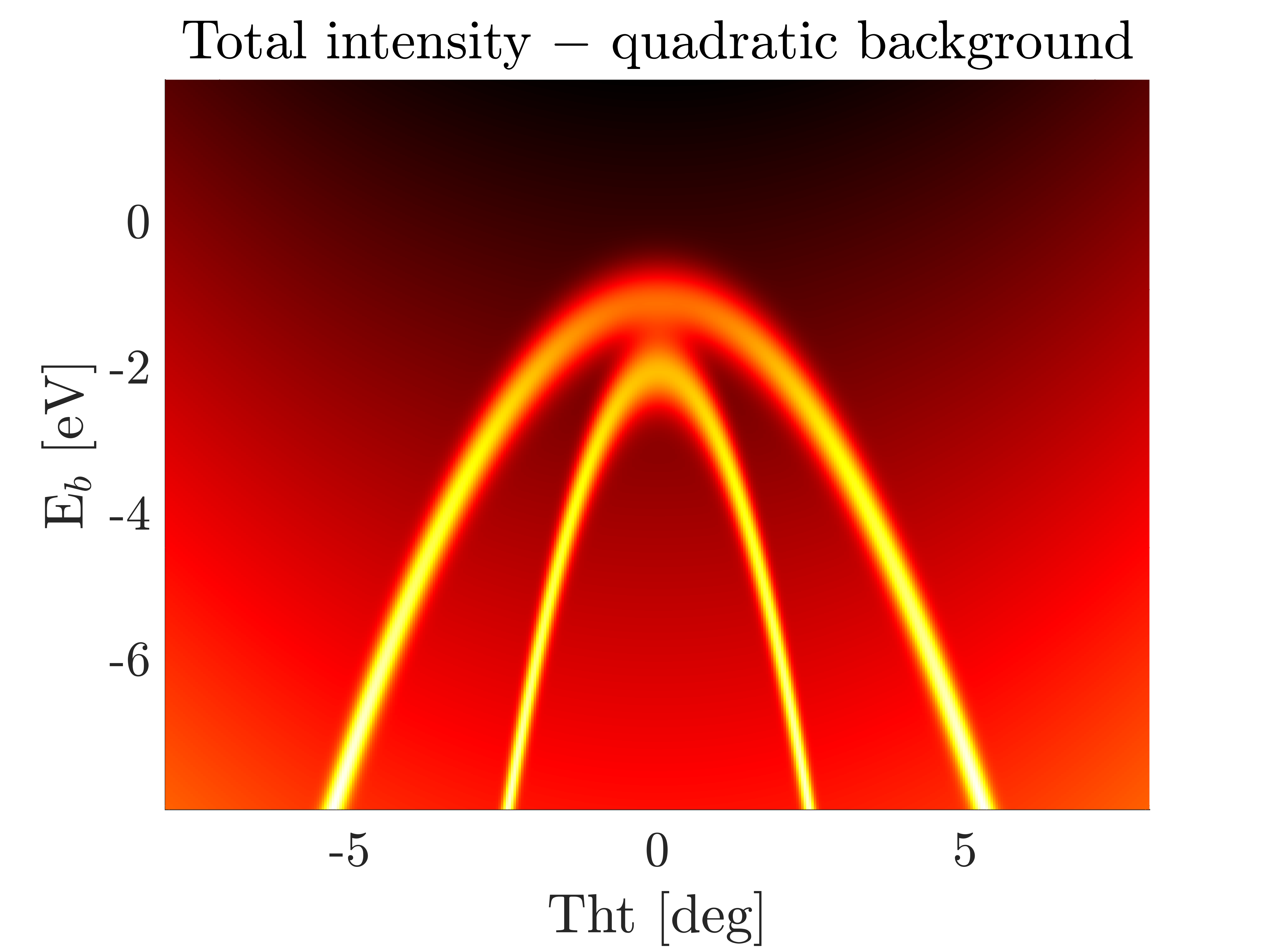
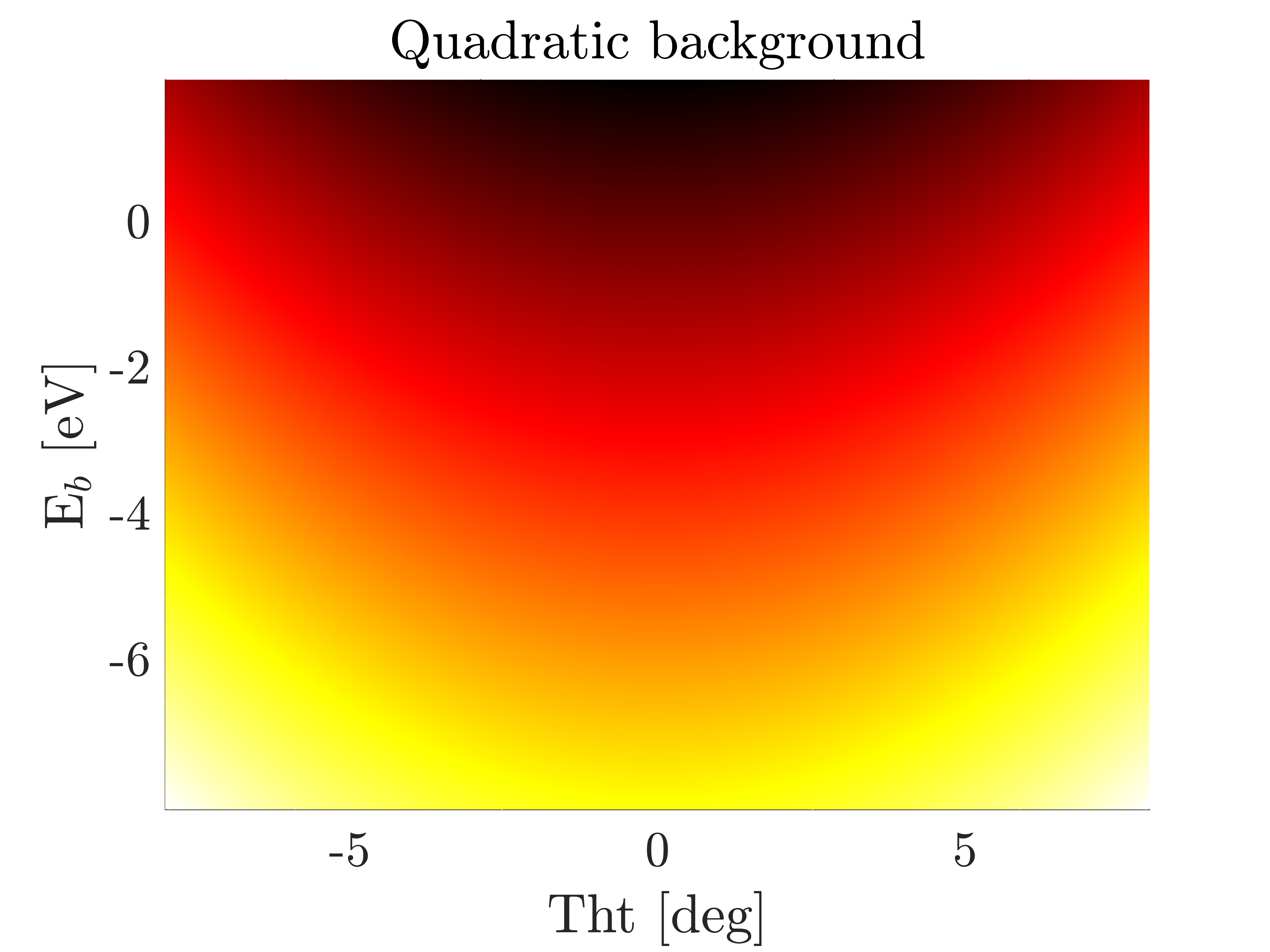
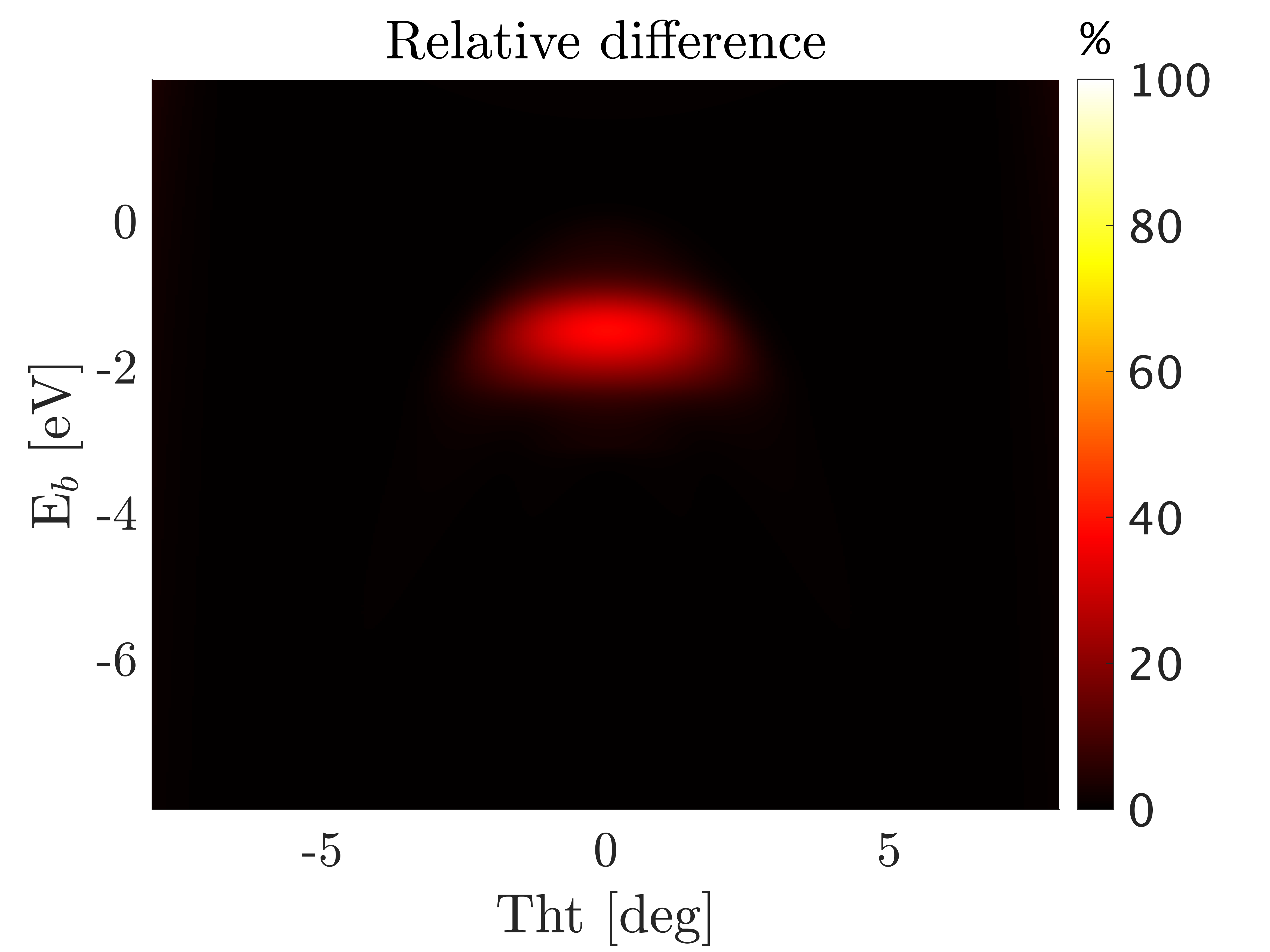
To judge the validity of this method, we constructed a data set similar to the measured spectra. The incoherent fraction of the constructed data set is known and can be directly compared with the extracted one. Fig. 5 shows the results obtained on the constructed spectra, using two types of background: linear and quadratic. In all these situations, the background subtraction algorithm proves to be extremely efficient. The only discrepancies are observed in the limit of zero band velocity and large effective mass, as Figs. 5 (c) and (f) show. This particular feature has been taken into account during the extraction of . For this reason, to obtain the , we excluded the region directly below the Fermi energy () and close to the point.
Appendix B Extraction of the coherence factor from ARPES data
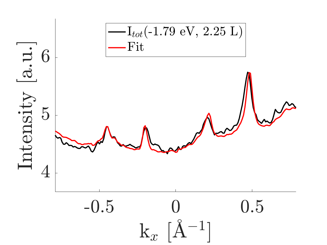
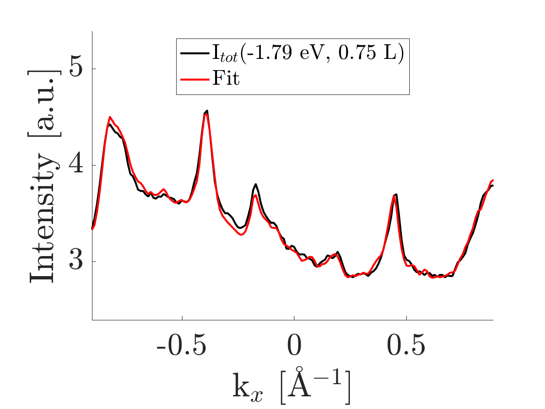
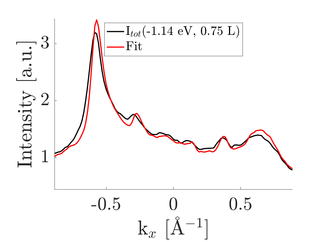
To obtain the , we fitted the coherent intensity measured after each sputtering cycle, with the coherent intensity extracted from the data measured on the cleaved sample. In particular, we extracted MDCs from the valence band region along KX, after background subtraction. Next, we optimized the parameter in the following equation:
| (5) |
where and are, respectively, the MDCs extracted from the total and incoherent intensities, centered at binding energy , measured on the sample after the sputtering dose . The parameter corresponds directly to and clearly depends on . For illustration purposes, Fig. 6 shows the results of this fitting procedure for .
Appendix C Coherence factor: fitted values
The optimal values , obtained by fitting vs. with Eq. 4, are displayed in the second column of Tab. 1. The third column shows the quantity .
| [eV] | [cm] | [cm-3L-1] |
|---|---|---|
References
- Strocov et al. [2019] V. N. Strocov, L. L. Lev, M. Kobayashi, C. Cancellieri, M. A. Husanu, A. Chikina, N. B. M. Schröter, X. Wang, J. A. Krieger, and Z. Salman, k-resolved electronic structure of buried heterostructure and impurity systems by soft-x-ray ARPES, Journal of Electron Spectroscopy and Related Phenomena 236, 1 (2019).
- Damascelli et al. [2003] A. Damascelli, Z. Hussain, and Z. Shen, Angle-resolved photoemission studies of the cuprate superconductors, Reviews of Modern Physics 75, 473 (2003).
- Powell [2020] C. J. Powell, Practical guide for inelastic mean free paths, effective attenuation lengths, mean escape depths, and information depths in x-ray photoelectron spectroscopy, Journal of Vacuum Science & Technology A 38, 023209 (2020).
- Kobayashi et al. [2012] M. Kobayashi, I. Muneta, T. Schmitt, L. Patthey, S. Ohya, M. Tanaka, M. Oshima, and V. N. Strocov, Digging up bulk band dispersion buried under a passivation layer, Applied Physics Letters 101, 242103 (2012), arXiv:1208.5767v1 .
- Strocov et al. [2014] V. N. Strocov, M. Kobayashi, X. Wang, L. L. Lev, J. Krempasky, V. V. Rogalev, T. Schmitt, C. Cancellieri, and M. L. Reinle-Schmitt, Soft-X-ray ARPES at the Swiss Light Source: From 3D Materials to Buried Interfaces and Impurities, Synchrotron Radiation News 27, 31 (2014).
- Woerle et al. [2017] J. Woerle, F. Bisti, M. A. Husanu, V. N. Strocov, C. W. Schneider, H. Sigg, J. Gobrecht, U. Grossner, and M. Camarda, Electronic band structure of the buried SiO2/SiC interface investigated by soft x-ray ARPES, Applied Physics Letters 110, 10.1063/1.4979102 (2017).
- Schuwalow et al. [2021] S. Schuwalow, N. B. M. Schröter, J. Gukelberger, C. Thomas, V. N. Strocov, J. Gamble, A. Chikina, M. Caputo, J. Krieger, G. C. Gardner, M. Troyer, G. Aeppli, M. J. Manfra, and P. Krogstrup, Band Structure Extraction at Hybrid Narrow‐Gap Semiconductor–Metal Interfaces, Advanced Science 8, 2003087 (2021).
- Yu et al. [2021] T. Yu, J. Wright, G. Khalsa, B. Pamuk, C. S. Chang, Y. Matveyev, X. Wang, T. Schmitt, D. Feng, D. A. Muller, H. G. Xing, D. Jena, and V. N. Strocov, Momentum-resolved electronic structure and band offsets in an epitaxial NbN/GaN superconductor/semiconductor heterojunction, Science Advances 7, 10.1126/sciadv.abi5833 (2021).
- Yang et al. [2022] S. Yang, N. B. M. Schröter, V. N. Strocov, S. Schuwalow, M. Rajpalk, K. Ohtani, P. Krogstrup, G. W. Winkler, J. Gukelberger, D. Gresch, G. Aeppli, R. M. Lutchyn, and N. Marom, Electronic Structure of InAs and InSb Surfaces: Density Functional Theory and Angle‐Resolved Photoemission Spectroscopy, Advanced Quantum Technologies 5, 2100033 (2022), 2012.14935 .
- Lutchyn et al. [2018] R. M. Lutchyn, E. P. A. M. Bakkers, L. P. Kouwenhoven, P. Krogstrup, C. M. Marcus, and Y. Oreg, Majorana zero modes in superconductor–semiconductor heterostructures, Nature Reviews Materials 3, 52 (2018).
- Sarma et al. [2015] S. D. Sarma, M. Freedman, and C. Nayak, Majorana zero modes and topological quantum computation, npj Quantum Information 1, 10.1038/npjqi.2015.1 (2015).
- Anderson [1959] P. Anderson, Theory of dirty superconductors, Journal of Physics and Chemistry of Solids 11, 26 (1959).
- Pendry [1976] J. Pendry, Theory of photoemission, Surface Science 57, 679 (1976).
- Feibelman and Eastman [1974] P. J. Feibelman and D. E. Eastman, Photoemission spectroscopy—correspondence between quantum theory and experimental phenomenology, Physical Review B 10, 4932 (1974).
- Mahan [1970] G. D. Mahan, Theory of photoemission in simple metals, Physical Review B 2, 4334 (1970).
- Schaich and Ashcroft [1970] W. Schaich and N. Ashcroft, Theory of photoemission, Solid State Communications 8, 1959 (1970).
- Braun et al. [2018] J. Braun, J. Minár, and H. Ebert, Correlation, temperature and disorder: Recent developments in the one-step description of angle-resolved photoemission, Physics Reports 740, 1 (2018).
- Inglesfield and Plummer [1992] J. Inglesfield and E. Plummer, Chapter 2 the physics of photoemission, in Angle-Resolved Photoemission - Theory and Current Applications (Elsevier, 1992) pp. 15–61.
- Henzler [1984] M. Henzler, Measurements of surface defects by low–energy electron diffraction, Applied Physics A 34, 205 (1984).
- Shevchik [1977] N. J. Shevchik, Disorder effects in angle-resolved photoelectron spectroscopy, Physical Review B 16, 3428 (1977).
- Shevchik and Liebowitz [1978] N. J. Shevchik and D. Liebowitz, Theory of angle-resolved photoemission from the bulk bands of solids. i. formalism, Physical Review B 18, 1618 (1978).
- Shevchik [1979] N. J. Shevchik, Theory of angle-resolved photoemission from the bulk bands of solids. III. effects of intra-atomic and interatomic electron-phonon interactions, Physical Review B 20, 3020 (1979).
- Strocov et al. [2010] V. N. Strocov, T. Schmitt, U. Flechsig, T. Schmidt, A. Imhof, Q. Chen, J. Raabe, R. Betemps, D. Zimoch, J. Krempasky, X. Wang, M. Grioni, A. Piazzalunga, and L. Patthey, High-resolution soft x-ray beamline ADRESS at the swiss light source for resonant inelastic x-ray scattering and angle-resolved photoelectron spectroscopies, Journal of Synchrotron Radiation 17, 631 (2010).
- Strocov et al. [2013] V. N. Strocov, X. Wang, M. Shi, M. Kobayashi, J. Krempasky, C. Hess, T. Schmitt, and L. Patthey, Soft-x-ray ARPES facility at the ADRESS beamline of the SLS: concepts, technical realisation and scientific applications, Journal of Synchrotron Radiation 21, 32 (2013).
- Braun et al. [2013] J. Braun, J. Minár, S. Mankovsky, V. N. Strocov, N. B. Brookes, L. Plucinski, C. M. Schneider, C. S. Fadley, and H. Ebert, Exploring the XPS limit in soft and hard x-ray angle-resolved photoemission using a temperature-dependent one-step theory, Physical Review B 88, 205409 (2013).
- Olsson et al. [1996] L. Ö. Olsson, C. B. M. Andersson, M. C. Håkansson, J. Kanski, L. Ilver, and U. O. Karlsson, Charge Accumulation at InAs Surfaces, Physical Review Letters 76, 3626 (1996).
- Lordi et al. [2010] V. Lordi, P. Erhart, and D. Åberg, Charge carrier scattering by defects in semiconductors, Physical Review B 81, 10.1103/physrevb.81.235204 (2010).
- Gunnarsson and Rösch [2008] O. Gunnarsson and O. Rösch, Interplay between electron–phonon and coulomb interactions in cuprates, Journal of Physics: Condensed Matter 20, 043201 (2008).
- Ziegler et al. [2010] J. F. Ziegler, M. Ziegler, and J. Biersack, SRIM – the stopping and range of ions in matter (2010), Nuclear Instruments and Methods in Physics Research Section B: Beam Interactions with Materials and Atoms 268, 1818 (2010).
- Aukerman [1968] L. Aukerman, Chapter 6 radiation effects, in Semiconductors and Semimetals (Elsevier, 1968) pp. 343–409.
- Hussain et al. [1980] Z. Hussain, C. S. Fadley, S. Kono, and L. F. Wagner, Temperature-dependent angle-resolved x-ray photoemission study of the valence bands of single-crystal tungsten: Evidence for direct transitions and phonon effects, Physical Review B 22, 3750 (1980).
- White et al. [1986] R. C. White, C. S. Fadley, M. Sagurton, and Z. Hussain, Angle-resolved x-ray photoemission from the valence bands of tungsten with high angular resolution and temperature variation, Physical Review B 34, 5226 (1986).
- Nicolaï and Minár [2018] L. Nicolaï and J. Minár, XPS limit in soft x-ray photoemission spectroscopy of ag(001), in AIP Conference Proceedings (Author(s), 2018).
- Soven [1967] P. Soven, Coherent-potential model of substitutional disordered alloys, Physical Review 156, 809 (1967).
- Sébilleau et al. [2018] D. Sébilleau, K. Hatada, and H. Ebert, eds., Multiple Scattering Theory for Spectroscopies (Springer International Publishing, 2018).
- Starnberg and Nilsson [1993] H. Starnberg and P. Nilsson, Thermal effects in angle-resolved photoemission: is it possible to separate direct and indirect transitions?, Surface Science 287-288, 776 (1993).
- Plucinski et al. [2008] L. Plucinski, J. Minár, B. C. Sell, J. Braun, H. Ebert, C. M. Schneider, and C. S. Fadley, Band mapping in higher-energy x-ray photoemission: Phonon effects and comparison to one-step theory, Physical Review B 78, 10.1103/physrevb.78.035108 (2008).
- Jain et al. [2013] A. Jain, S. P. Ong, G. Hautier, W. Chen, W. D. Richards, S. Dacek, S. Cholia, D. Gunter, D. Skinner, G. Ceder, and K. A. Persson, Commentary: The materials project: A materials genome approach to accelerating materials innovation, APL Materials 1, 10.1063/1.4812323 (2013).
- Gray et al. [2011] A. X. Gray, C. Papp, S. Ueda, B. Balke, Y. Yamashita, L. Plucinski, J. Minár, J. Braun, E. R. Ylvisaker, C. M. Schneider, W. E. Pickett, H. Ebert, K. Kobayashi, and C. S. Fadley, Probing bulk electronic structure with hard x-ray angle-resolved photoemission, Nature Materials 10, 759 (2011).
- Tanuma et al. [2011] S. Tanuma, C. J. Powell, and D. R. Penn, Calculations of electron inelastic mean free paths. IX. data for 41 elemental solids over the 50 eV to 30 keV range, Surface and Interface Analysis 43, 689 (2011).
- Mahan [2000] G. D. Mahan, Many-Particle Physics (Springer US, 2000).
- Strocov [2003] V. N. Strocov, Intrinsic accuracy in 3-dimensional photoemission band mapping, Journal of Electron Spectroscopy and Related Phenomena 130, 65 (2003).