Half-Valley Ohmic Contact and
Contact-Limited Valley-Contrasting Current Injection
Abstract
Two-dimensional (2D) ferrovalley semiconductor (FVSC) with spontaneous valley polarization offers an exciting material platform for probing Berry phase physics. How FVSC can be incorporated in valleytronic device applications, however, remain an open question. Here we generalize the concept of metal/semiconductor (MS) contact into the realm of valleytronics. We propose a half-valley Ohmic contact based on FVSC/graphene heterostructure where the two valleys of FVSC separately forms Ohmic and Schottky contacts with those of graphene, thus allowing current to be valley-selectively injected through the ‘Ohmic’ valley while being blocked in the ‘Schottky’ valley. We develop a theory of contact-limited valley-contrasting current injection and demonstrate that such transport mechanism can produce gate-tunable valley-polarized injection current. Using RuCl2/graphene heterostructure as an example, we illustrate a device concept of valleytronic barristor where high valley polarization efficiency and sizable current on/off ratio, can be achieved under experimentally feasible electrostatic gating conditions. These findings uncover contact-limited valley-contrasting current injection as an efficient mechanism for valley polarization manipulation, and reveals the potential of valleytronic MS contact as a functional building block of valleytronic device technology.
I Introduction
Valleytronics is an emerging device concept that harnesses the valley degree of freedom for information encoding and processing [1, 2, 3, 4, 5, 6, 7, 8, 9]. Valley-contrasting phenomena, such as anomalous valley hall effect (AVHE) [10], has been studied extensively in two-dimensional (2D) materials [11, 12, 13], and can be generated via a plethora of structural [7, 14, 15, 16, 17], electrical [9, 18], mechanical [19, 20], magnetic [21, 22, 23, 24], and optical [25, 26] mechanisms. Recent discovery of ferrovalley semiconductor (FVSC) [27] unveils an exciting platform to study valley-constrating phenomena and Berry phase physics in the 2D flatland. Due to the simultaneous breaking of spatial inversion and time reversal symmetries, the and valley degeneracy is broken in FVSC, and valley polarization emerges spontaneously without any external regulating mechanisms [28, 29, 30, 31, 32, 33, 34, 35, 36, 37, 38, 39].
The spontaneous valley polarization in FVSC [40, 41] is particularly much sought after for producing valley polarized current (VPC) – an electrical current with carriers dominantly from only one valley. Despite tremendous efforts in the search for FVSC candidates and the high anticipation of FVSC as a building block of valleytronics, the questions of (i) how FVSC forms contact with metal electrodes – an omnipresent component of modern electronics; (ii) how contact-limited charge injection occur [42, 43]; and (iii) how FVSC/metal contact can be incorporated in the design of valleytronic devices remain largely open thus far [44].
In this work, we addressed the above questions by generalizing the conventional MS contact into the realm of valleytronics. We show that the synergy of FVSC and metal contact can achieve efficient valley degree of freedom manipulation. We propose the concept of half-valley Ohmic contact in which the and valleys of FVSC separately forms Schottky and Ohmic contacts with a contacting metal of matching and valleys. Electrical current can be injected through the ‘Ohmic valley’ while being suppressed at the ‘Schottky valley’. We develop a model of contact-limited valley-contrasting current injection across graphene/FVSC, and show that such process provides a mechanism to manipulate the valley polarization of the injection current. Using graphene/RuCl2 contact heterostructures as a model example, the material realization of half-valley Ohmic contact is demonstrated. We propose a device concept of valleytronic barristor (i.e. ‘barrier’ + ‘transistor’ [45]) in which the injection current can be switched on and off, and the VPC can be tuned all-electrically under experimentally feasible electrostatic gating conditions. Our findings unveil a wealth of MS contact species, notably the half-valley Ohmic contact, which emerges when generalizing the concept of MS contact into the valleytronic realm. The half-valley Ohmic contact proposed in this work shall provide a useful functional building block of valleytronic devices, and shall serve as a harbinger for a new class of valleytronic devices that manipulates valley degree of freedom via contact-limited valley-contrasting charge injection process.
II Results and Discussion
II.1 Concept of Half-Valley Ohmic Contact
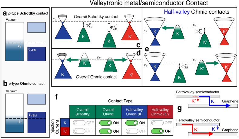
When a metal is brought into contact with a semiconductor [46], a Schottky or Ohmic MS contact is formed dependent on the relative alignment of the semiconductor band edges and the metal Fermi level . In the case of -type MS contact, a Schottky contact is formed if the metal Fermi level is energetically higher than the valence band maximum (VBM) of the semiconductor (Fig. 1a). The presence of a potential barrier, known as the Schottky barrier (SB), energetically separate the valence band electronic states from the unoccupied states around the Fermi level in the metal, forming a current-blocking Schottky contact. Conversely, if the VBM is higher than the metal Fermi level, the electronic states in semiconductor valence band matches a large abundance of unoccupied states around the metal Fermi level, giving rise to Ohmic contact that allows efficient charge injection across the MS contact (Fig. 1b).
In FVSC, the valence band edges at and points of the Brillouine zone are composed of electronic states residing exclusively in or ’ valleys, respectively. The valence band valley offset of where is the magnitude of the band edge energy of or valley, respectively, relative to the Fermi level. Such valley offset creates a wealth of band alignments at a FVSC/metal contact. For instance, consider a MS contact composed of FVSC and monolayer graphene which host a matching and valleys to those of the FVSC. The concept of conventional MS contact can be generalized to such valleytronic case, yielding three distinct types contact types (see Figs. 1c to 1d):
(i) Overall Schottky contact:- The band edges of and valleys of FVSC are both lower than the graphene Fermi level, thus resulting in an overall Schottky contact (1c) with finite Schottky barrier height (SBH) in both valleys;
(ii) Overall Ohmic contact:- The band edges of and valleys of FVSC are both higher than the graphene Fermi level, thus resulting in overall Ohmic contact with zero SBH in both valleys (1d);
(iii) Half-valley Ohmic contact:- Intriguingly, if the band edge energy of only one valley is higher than while that of the opposite valley is lower than , such MS contact forms a peculiar hybrid contact type in which one valley forms Ohmic contact with graphene while the opposite valley forms Schottky contact with graphene (1e). We regard this contact type as the half-valley Ohmic contact, which represents a unique hallmark of valleytronic MS contacts.
Importantly, current injection is only allowed in one valley of a half-valley Ohmic contact, while being strongly suppressed in the opposite valley (1f). Valley-contrasting current injection can thus be injected across the FVSC/graphene contact through a half-valley Ohmic FVSC-based MS contact (Fig. 1g). As demonstrated below, electrostatic contact gating [47, 48] can be utilized to externally tune the band alignment between FVSC band edge energies and graphene Fermi level, thus enabling the FVSC/graphene contact to be switched between various valleytronic contact types. The valleytronic generalization of MS contact proposed in Fig. 1 thus provide a versatile platform to achieve contact-limited valley-contrasting carrier injection - a previously unexplored mechanism to manipulate the valley polarization of the electrical current.
II.2 Candidate 2D Ferrovalley Semiconductors: RuCl2
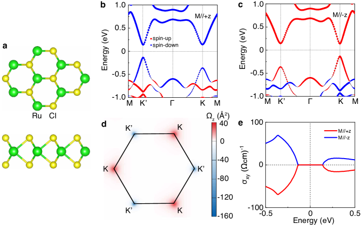
To illustrate the concept of half-valley Ohmic contact, we consider FVSC RuCl2 monolayer (see Fig. 2a for the lattice structures) as the candidate FVSC due to its large spontaneous valley polarization meV (see Figs. 2b and 2c for the band structures under opposite magnetization directions) [36, 37]. The calculated lattice constants of RuCl2 monolayer is 3.50 Å, which is consistent with previous studies [36, 37]. Valley-contrasting transport, such as AVHE [27], emerges due to the presence of nontrivial Berry curvature in the phase space, which can be calculated as
| (1) |
where is the Fermi-Dirac distribution function, are the velocity operators along the / directions, is the band energy. The Berry curvatures of both structures possess unequal absolute values with opposite signs at and points (Fig. 2d) for RuCl2 - a distinctive hallmark of FVSC.
Carriers residing in the two valleys acquire a valley-contrasting anomalous velocity under an external in-plane electric field ,
| (2) |
in which their opposite transversal motion leads to VAHE – an exotic transport phenomenon that is practically useful for information processing and storage applications [48] in addition to probing the fundamental Berry phase physics of FVSC. When the out-of-plane magnetization is reversed such as via spin-orbit torque effect [49], the spontaneous valley polarization (see Figs. 2b and c for the band structures under different magnetization direction) and the anomalous hall conductivity (Fig. 2e) of RuCl2 can thus be fully reversed externally via magnetic tuning knob, such as ferromagnetic substrate [50, 51].
II.3 Material Realization of Half-Valley Ohmic Contact: RuCl2/Graphene Heterostructure
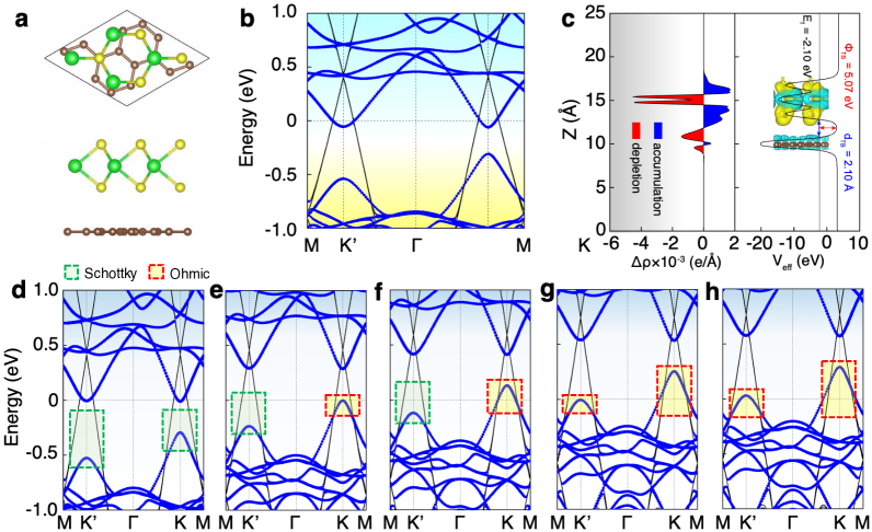
Monolayer RuCl2 pertains the point group, which is similar to that of graphene, thus ensuring a good lattice matching with graphene – a 2D semimetal with similar and . We construct a valleytroinc MS heterostructures using supercells of RuCl2 combined with supercell of graphene (Fig. 3a), which yields a lattice constant of 7.00 Å and a interlayer distance of Å in the fully relaxed heterostructure. To verify the energetic stability of the heterostructures, the binding energy is calculated as
| (3) |
where is the atom number of the heterostructure, and , as well as are the energy of the contact heterostructure, isolated FVSC and isolated graphene, respectively. The binding energy of RuCl2/graphene is meV/supercell, respectively, thus indicating the energetic feasiblity of the heterostructures.
The band structure of RuCl2/graphene is shown in Fig. 3b. A sizable valley polarization of 231 meV is retained the electronic structures of RuCl2 sub-monolayer, which is about with reference to room temperature, thus satisfying room temperature operation requirement. Importantly, RuCl2/graphene has a ‘clean’ ideal two-valley band structures where the the lower-energy valley is not energetically ‘buried’ below other hole bands. This aspect is in stark contrast to many other non-ideal FVSCs, such as NbSe2, in which the hole pocket at the point could lead to non-valley signal that masks out the valleytronic signatures from the and valleys (for example, see Fig. S1 in the SI for band structure calculation of NbSe2/graphene heterostructure in which the -point VBM is undesirably higher than one of the valleys). RuCl2/graphene is thus a promising system to realize the half-Ohmic valley contact.
RuCl2/graphene heterostructure is intrinsically a non-valleytronic -type Ohmic contact. As the work function of RuCl2 is 5.99 eV, which is higher than the work function of graphene [47], significant electrons transfer from graphene to RuCl2 occurs. This results in -type characteristics of graphene while RuCl2 gains electrons to form -type contact. The charge transfer process is also revealed in the planar-averaged differential charge density in Fig. 3c in which electron accumulation (depletion) on the RuCl2 (graphene) side is evident. A van der Waals gap is present between the two constituent monolayers leads which can be characterized by a plane-averaged tunneling potential barrier [52] of height eV and width Å.
Although the RuCl2/Gr heterostructure is intrinsically an -type contact, electrostatic doping through an external gate voltage can transform the system into -type half-valley Ohmic contact. Hole doping, which can be induced by an external gate voltage [53, 54, 48], energetically up-shifts the band structure of RuCl2/graphene heterostructure, thus enabling the contact type to be modulated from -type to -type. Such modulation effect is demonstrated in Figs. 3d to 3h where the doping levels are increased from 0.1 to 0.5 hole per supercell. The band structure evolves progressively from -type Ohmic -type half Ohmic to -type overall Ohmic contacts. The -type half valley Ohmic contact is achieved at a moderate doping level of 0.3 hole per supercell (Fig. 3f) while -type overall Ohmic contact can be achieved when the doping level exceeds 0.4 hole per supercell. Such doping-controlled contact types of RuCl2/graphene heterostructure can be harnessed to achieve gate-tunable valley-polarized current, thus suggesting FVSC/graphene as a versatile building block of valleytronics device applications.
II.4 Theory of Contact-Limited Valley Current Injection
We now develop a model of contact-limited current injection across a valleytronic MS contact and demonstrate how such injection process enables valley-polarized current to flow across a FVSC/graphene heterostructure. We consider the case where a bias voltage is applied at graphene. The net valence band electrical injection current via a single valley (i.e. or valley) can be expressed as [42, 55]
| (4) |
where the superscript () denotes () valley, is the spin degeneracy, is the valley-dependent SBH relative to graphene Fermi level (), is the in-plane 2D wave vector of electrons, is the out-of-plane carrier injection time parameter [56, 57] which is material-and device-dependent, and are the carrier distribution function of graphene and FVSC, respectively, with being the equilibrium Fermi-Dirac distribution function. For over-barrier thermionic emission, the tunneling probability is where is the Heaviside step function.
Consider isotropic energy dispersion, which is appropriate for graphene and RuCl2, Eq. (4) becomes
| (5) |
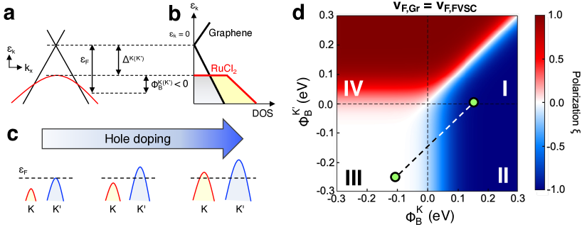
where we have taken the Dirac point of graphene as the zero-energy, and . The electronic density of states (DOS) term is defined as since the transport current is limited by the constituent monolayer that has the smaller DOS (Figs. 4a and 4b). The DOS of graphene and FVSC are and , respectively. The Fermi velocity parameters are extracted from the DFT-calculated band structure as m/s and m/s for graphene and RuCl2, respectively. As , the DOS of RuCl2 is larger than that of graphene due to the ‘flatter’ energy dispersion of the gapped Dirac cone of RuCl2 (Fig. 4b). The injection current thus becomes graphene-limited, and can be reduced to
| (6) |
Generally, the valley injection current increases with smaller . As demonstrated in Figs. 3d to 3h, electrostatic hole doping of the graphene/RuCl2 heterostructure results in the up-shifting of the and bands, which transforms the heterostructure from half-valley Ohmic to overall Ohmic contacts (Fig. 4c). To how modulation affect the valley-contrasting charge injection in the graphene/FVSC heterostructure, we calculate the valley polarization phase diagram with varying from -0.3 to 0.3 eV (Fig. 4e), which is defined as
| (7) |
In Fig. 4d, the quadrants II and IV represent the cases of half-valley Ohmic contact (i.e. and ) have opposite signs) which exhibits large K’ and K valley polarization, respectively. Quadrant I corresponds to the case of overall Schottky contact (i.e. overall Schottky (i.e. both and are positive-valued). Here the the injection current of the two ‘Schottky’ valleys compete with each others, resulting in a sharp reversal of the valley polarization reverses between the regime of and . Interestingly, the valley polarization can be switched off in the quadrant III as both valleys are Ohmic, i.e. overall Ohmic in which and . Considering a half-valley Ohmic contact with representative SBH values of eV and eV and undergoes the SBH modulation via hole doping as indicated in Fig. 4c, and assuming that the energy difference between the and valley VBM remains approximately the same during the SBH modulation, the and evolve along a linear path in the - as indicated by the dashed line in Fig. 4e. The valley polarization is switched off during the electrostatic hole doping, thus suggesting that the valley polarization of a valleytronic MS junction can be manipulated by an electrostatic gate.
II.5 Device Concept and Operation Characteristics of Valleytronic Barristor
We now demonstrate the valley polarization switching effect based on the DFT simualtion results of graphene/RuCl2. Figure 5a shows the schematic drawing of a valleytronic barristor in which two key functions can be achieved electrostatically via a gate voltage: (i) the valley polarization can be tuned and reserved (ii) the injection current can be switched on and off. Such gate-tunable operation arises mainly from the electrostatic doping-controlled SBH in the and valleys as described in Figs. 3e to 3h. It should be noted that the practicality of the electrostatic doping in graphene/RuCl2 is ultimately limited by the gate dielectric breakdown strength. To estimate whether the required carrier doping concentration can be achieved within the dielectric breakdown limit of the gate insulators, we employ a planar diode model to obtain the electric displacement field [58],
| (8) |
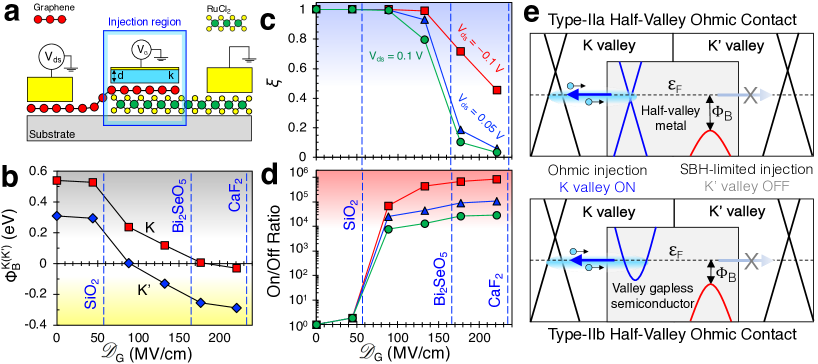
where is the gate voltage, is the dielectric thickness, is the dielectic constant of the dielectric material and is the electrostatically induced carrier density in the heterostructure. Here, is calculated as the added electron per unit supercell area employed in Figs. 3d to 3h (i.e. 0.1 to 0.5 electron added per unit supercell area). The corresponding to 0.1 to 0.5 hole doping ranges from about 44 MV/cm to 221 MV/cm (see Table S1 for a list of the values). The is related to the actual electric field across the gate dielectric via . The can thus be scaled down with high- gate dielectrics. Furthermore, dielectric breakdown limits the maximum hole doping concentration, giving rise to the condition, where is the electric displacement at the breakdown field of the gate dielectric (). Equivalently, corresponds to the maximum carrier density that can be provided by a gate dielectric is [59]. We consider several representative oxide dielectric materials, namely the (, MV/cm) widely used in CMOS technology [60], as well as the recently experimentally synthesized single-crystalline layered insulator Bi2SeO5 (, MV/cm) [61] and ultrathin CaF2 ionic crystals (, MV/cm) [62]. Correspondingly, the breakdown electric displacement fields are MV/cm for SiO2, Bi2SeO5 and CaF2, respectively.
The and are extracted from the DFT-calculated band structures in Figs. 3d to 3h. The simulated transport characteristics are shown in Figs. 5b to 5d. The gate dielectric breakdown limits, i.e. , are marked on Figs. 5b to 5d. The of all hole doping cases can be accommodated by CaF2, thus suggesting a potential experimental feasibility of the electrostatic doping approach in modulating the -and -valley SBH (Fig. 5b). Using the contact-limited valley-contrasting current injection model developed above (see Eq. 7), we show in Fig. 5b that the valley polarization can achieved polarization efficiency and can be tuned towards with higher , thus revealing contact-limited valley-contrasting injection as an effective mechanism to modulate the valley polarization. Importantly, Fig. 5d shows that the injection current can exhibit sizable ON/OFF ratio, defined as where and are the total injection injection with and without hole doping, respectively. Generally, a higher hole doping level (i.e. higher ) leads to a more metallic behavior of the contact heterostructure, thus leading to a higher ON/OFF ratio at high . An ON/OFF ratio of and above can be achieved. Figures 5c to 5d suggest that graphene/RuCl2 heterostructure can function as a valleytronic barristor in which both the current on/off switching and the valley polarization modulation can be achieved via electrostatic contact gating. It should be noted that MV/cm is sufficient to switch the device into ON state while still maintaining high valley polarization (Figs. 5c and 5d). Such a value is well within the breakdown limit of Bi2SeO5 [61] and CaF2 [62] whose integration with 2D semiconductor devices have been recently demonstrated experimentally [63].
Finally, we remark that the half-valley Ohmic contact proposed here can also be achieved using half-valley metal (HVM) [64, 65], half-valley semiconductor (HVSC) [66] and valley gapless semiconductor (VGSC) [67]. Figure 5f schematically illustrate the concept of graphene/HVM contact and graphene/VGSC, which can be regarded as the type-II half-valley Ohmic contacts due to the gapless nature of the band structures. The gapless valley of the HVM provides barrier-less Ohmic injection into graphene with high injection current, while the injection current through the gapped valley is severely suppressed by the Schottky barrier. In the VGSC counterpart, the K valley exhibits -type Ohmic contact while the K’ valley exhibits -type Schottky contact, which similarly exhibits contact-limited valley contrasting charge injection. The possibility of achieving contact-limited valley-contrasting carrier injection using a large variety of valleytronic materials, covering FVSC, HVM and HVSC, suggest the versatility of half-valley Ohmic contact as a potential platform for valleytronics device applications.
III Conclusion
In summary, we generalized the concept of metal/semiconductor (MS) contact into the valleytronics scenario. We proposed the concept of half-valley Ohmic contact in graphene/ferrovalley semiconductor (FVSC) heterostructure and proposed its material realization using RuCl2/graphene heterostructure. We developed the theory of contact-limited valley-contrasting charge injection for valleytronic MS contact, and proposed a design of valleytronic barristor in which the valley polarization and the injection current can be switched via a gate voltage under experimentally realizable electrostatic gating conditions. The proposed half-valley Ohmic contact can potentially be realized in valleytronic materials beyond FVSC, such as half-valley metal and valley gapless semiconductor. Our findings revealed the radically different MS contact types in valleytronic materials, and provided a theoretical basis to describe the charge injection process in such contacts. The half-valley Ohmic contact proposed in this work shall provide a useful building block for the development of valleytronic device technology, and shall serve as a harbinger for a new class of valleytronic devices that manipulates valley degree of freedom via contact-limited valley-contrasting charge injection process.
Methods
III.1 Computational Methods
All density functional theory (DFT) calculations are performed in Vienna Ab-initio Simulation Package (VASP) [68, 69] using projector augmented wave (PAW) method [70]. The generalized gradient approximation (GGA) with Perdew-Burke-Ernzerhof (PBE) type functional [71, 72] is adopted to treat the exchange-correlation interactions between electrons. The GGA+U scheme is adopted to deal with the strong exchange-correlation interactions for Ru- orbital. The effective Hubbard parameter are set as 2.0 eV for as implemented in previous work [36]. The kinetic energy is cut off at 500 eV. The 2D reciprocal space is sampled with the Monkhorst-Pack (MP) grid [73] of . The structures are relaxed until the force on each atom converged to 0.001 eV/Å and the energy convergence criterion is eV. A vacuum of 20 Å is applied to eliminate interactions between adjacent layers. The van der Waals interactions is also considered utilizing DFT-D3 approach [74]. The Berry curvature and anomalous all conductivity are calculated using WannierTools Package[75] with tight binding Hamiltonian extracted by WANNIER90 package [76].
Acknowledgements.
This work is supported by the Singapore Ministry of Education Academic Research Fund Tier 2 (Award No. MOE-T2EP50221-0019) and the SUTD-ZJU IDEA Thematic Research Grant Exploratory Project (SUTD-ZJU (TR) 202203). The computational work for this article was partially performed on resources of the National Supercomputing Centre, Singapore (https://www.nscc.sg).References
- Xiao et al. [2007] D. Xiao, W. Yao, and Q. Niu, Phys. Rev. Lett. 99, 236809 (2007).
- Yao et al. [2008] W. Yao, D. Xiao, and Q. Niu, Phys. Rev. B 77, 235406 (2008).
- Xiao et al. [2012] D. Xiao, G.-B. Liu, W. Feng, X. Xu, and W. Yao, Phys. Rev. Lett. 108, 196802 (2012).
- Liu et al. [2015] G.-B. Liu, D. Xiao, Y. Yao, X. Xu, and W. Yao, Chem. Soc. Rev. 44, 2643 (2015).
- Schaibley et al. [2016] J. R. Schaibley, H. Yu, G. Clark, P. Rivera, J. S. Ross, K. L. Seyler, W. Yao, and X. Xu, Nat. Rev. Mater. 1, 1 (2016).
- Li et al. [2013] X. Li, T. Cao, Q. Niu, J. Shi, and J. Feng, Proc. Natl. Acad. Sci. USA 110, 3738 (2013).
- Rycerz et al. [2007] A. Rycerz, J. Tworzydło, and C. Beenakker, Nature Physics 3, 172 (2007).
- Li et al. [2020a] L. Li, L. Shao, X. Liu, A. Gao, H. Wang, B. Zheng, G. Hou, K. Shehzad, L. Yu, F. Miao, et al., Nat. Nanotechnol. 15, 743 (2020a).
- Ang et al. [2017] Y. S. Ang, S. A. Yang, C. Zhang, Z. Ma, and L. K. Ang, Phys. Rev. B 96, 245410 (2017).
- Mak et al. [2014] K. F. Mak, K. L. McGill, J. Park, and P. L. McEuen, Science 344, 1489 (2014).
- Mak et al. [2010] K. F. Mak, C. Lee, J. Hone, J. Shan, and T. F. Heinz, Phys. Rev. Lett. 105, 136805 (2010).
- Wang et al. [2012] Q. H. Wang, K. Kalantar-Zadeh, A. Kis, J. N. Coleman, and M. S. Strano, Nat. Nanotechnol. 7, 699 (2012).
- Goh et al. [2023] K. E. J. Goh, C. P. Y. Wong, and T. Wang, Valleytronics in 2D materials (World Scientific, 2023).
- Zhu et al. [2012] Z. Zhu, A. Collaudin, B. Fauqué, W. Kang, and K. Behnia, Nat. Phys. 8, 89 (2012).
- Ju et al. [2015] L. Ju, Z. Shi, N. Nair, Y. Lv, C. Jin, J. Velasco, C. Ojeda-Aristizabal, H. A. Bechtel, M. C. Martin, A. Zettl, et al., Nature 520, 650 (2015).
- Yu et al. [2020] Z.-M. Yu, S. Guan, X.-L. Sheng, W. Gao, and S. A. Yang, Phys. Rev. Lett. 124, 037701 (2020).
- Zhang et al. [2022] T. Zhang, X. Xu, B. Huang, Y. Dai, and Y. Ma, npj Comput. Mater. 8, 64 (2022).
- Tao and Tsymbal [2019] L. Tao and E. Y. Tsymbal, Phys. Rev. B 100, 161110 (2019).
- Ghaemi et al. [2012] P. Ghaemi, J. Cayssol, D. N. Sheng, and A. Vishwanath, Phys. Rev. Lett. 108, 266801 (2012).
- Fujita et al. [2010] T. Fujita, M. B. A. Jalil, and S. G. Tan, Appl. Phys. Lett. 97, 043508 (2010).
- Cheng et al. [2014] Y. Cheng, Q. Zhang, and U. Schwingenschlögl, Phys. Rev. B 89, 155429 (2014).
- Zhang et al. [2016] Q. Zhang, S. A. Yang, W. Mi, Y. Cheng, and U. Schwingenschlögl, Adv. Mater. 28, 959 (2016).
- Peng et al. [2018] R. Peng, Y. Ma, S. Zhang, B. Huang, and Y. Dai, J. Phys. Chem. Lett. 9, 3612 (2018).
- Li et al. [2018] J. Li, R.-X. Zhang, Z. Yin, J. Zhang, K. Watanabe, T. Taniguchi, C. Liu, and J. Zhu, Science 362, 1149 (2018).
- Zeng et al. [2012] H. Zeng, J. Dai, W. Yao, D. Xiao, and X. Cui, Nat. Nanotechnol. 7, 490 (2012).
- Bussolotti et al. [2023] F. Bussolotti, T. Maddumapatabandi, and K. Goh, Materials for Quantum Technology 3, 032001 (2023).
- Tong et al. [2016] W.-Y. Tong, S.-J. Gong, X. Wan, and C.-G. Duan, Nat. Commun. 7, 1 (2016).
- Zhang et al. [2019] C. Zhang, Y. Nie, S. Sanvito, and A. Du, Nano Lett. 19, 1366 (2019).
- Luo et al. [2020] C. Luo, X. Peng, J. Qu, and J. Zhong, Phys. Rev. B 101, 245416 (2020).
- Hu et al. [2020a] H. Hu, W.-Y. Tong, Y.-H. Shen, X. Wan, and C.-G. Duan, npj Comput. Mater. 6, 1 (2020a).
- Zhao et al. [2019] P. Zhao, Y. Ma, C. Lei, H. Wang, B. Huang, and Y. Dai, Appl. Phys. Lett. 115, 261605 (2019).
- Peng et al. [2020] R. Peng, Y. Ma, X. Xu, Z. He, B. Huang, and Y. Dai, Phys. Rev. B 102, 035412 (2020).
- Cheng et al. [2021] H.-X. Cheng, J. Zhou, W. Ji, Y.-N. Zhang, and Y.-P. Feng, Phys. Rev. B 103, 125121 (2021).
- Zang et al. [2021] Y. Zang, Y. Ma, R. Peng, H. Wang, B. Huang, and Y. Dai, Nano Res. 14, 834 (2021).
- Wang et al. [2020] B. Wang, X. Zhang, Y. Zhang, S. Yuan, Y. Guo, S. Dong, and J. Wang, Mater. Horiz. 7, 1623 (2020).
- Sheng et al. [2022] K. Sheng, B. Zhang, H.-K. Yuan, and Z.-Y. Wang, Phys. Rev. B 105, 195312 (2022).
- Li et al. [2022] R. Li, N. Mao, X. Wu, B. Huang, Y. Dai, and C. Niu, Nano Lett. (2022).
- He et al. [2021] Z. He, R. Peng, X. Feng, X. Xu, Y. Dai, B. Huang, and Y. Ma, Physical Review B 104, 075105 (2021).
- Feng et al. [2022] X. Feng, Z. He, R. Peng, Y. Dai, B. Huang, and Y. Ma, Physical Review Materials 6, 044001 (2022).
- MacNeill et al. [2015] D. MacNeill, C. Heikes, K. F. Mak, Z. Anderson, A. Kormányos, V. Zólyomi, J. Park, and D. C. Ralph, Phys. Rev. Lett. 114, 037401 (2015).
- Li et al. [2020b] L. Li, S. Jiang, Z. Wang, K. Watanabe, T. Taniguchi, J. Shan, and K. F. Mak, Phys. Rev. Mater. 4, 104005 (2020b).
- Ang et al. [2018] Y. S. Ang, H. Y. Yang, and L. Ang, Phys. Rev. lett. 121, 056802 (2018).
- Ang et al. [2021] Y. S. Ang, L. Cao, and L. K. Ang, InfoMat 3, 502 (2021).
- Bussolotti et al. [2018] F. Bussolotti, H. Kawai, Z. E. Ooi, V. Chellappan, D. Thian, A. L. C. Pang, and K. E. J. Goh, Nano Futures 2, 032001 (2018).
- Yang et al. [2012] H. Yang, J. Heo, S. Park, H. J. Song, D. H. Seo, K.-E. Byun, P. Kim, I. Yoo, H.-J. Chung, and K. Kim, Science 336, 1140 (2012).
- Tung [2014] R. T. Tung, Appl. Phys. Rev. 1, 011304 (2014).
- Yu et al. [2009] Y.-J. Yu, Y. Zhao, S. Ryu, L. E. Brus, K. S. Kim, and P. Kim, Nano lett. 9, 3430 (2009).
- Xiao et al. [2020] J. Xiao, Y. Wang, H. Wang, C. Pemmaraju, S. Wang, P. Muscher, E. J. Sie, C. M. Nyby, T. P. Devereaux, X. Qian, et al., Nature Physics 16, 1028 (2020).
- Li et al. [2016] P. Li, T. Liu, H. Chang, A. Kalitsov, W. Zhang, G. Csaba, W. Li, D. Richardson, A. DeMann, G. Rimal, et al., Nat. Commun. 7, 1 (2016).
- Wei et al. [2016] P. Wei, S. Lee, F. Lemaitre, L. Pinel, D. Cutaia, W. Cha, F. Katmis, Y. Zhu, D. Heiman, J. Hone, et al., Nature materials 15, 711 (2016).
- Bora and Deb [2021] M. Bora and P. Deb, Journal of Physics: Materials 4, 034014 (2021).
- Tho et al. [2023] C. C. Tho, C. Yu, Q. Tang, Q. Wang, T. Su, Z. Feng, Q. Wu, C. Nguyen, W.-L. Ong, S.-J. Liang, et al., Adv. Mater. Interfaces 10, 2201856 (2023).
- Zhang et al. [2020] X. Zhang, T. Zhu, J. Huang, Q. Wang, X. Cong, X. Bi, M. Tang, C. Zhang, L. Zhou, D. Zhang, et al., ACS Applied Materials & Interfaces 12, 46900 (2020).
- Chen et al. [2020] K. Chen, J. Deng, Q. Shi, X. Ding, J. Sun, S. Yang, and J. Z. Liu, Nanoscale 12, 12541 (2020).
- Somvanshi et al. [2017] D. Somvanshi, S. Kallatt, C. Venkatesh, S. Nair, G. Gupta, J. K. Anthony, D. Karmakar, and K. Majumdar, Phys. Rev. B 96, 205423 (2017).
- Sinha and Lee [2014] D. Sinha and J. U. Lee, Nano lett. 14, 4660 (2014).
- Javadi et al. [2020] M. Javadi, A. Noroozi, and Y. Abdi, Phys. Rev. Appl. 14, 064048 (2020).
- Xia et al. [2010] F. Xia, D. B. Farmer, Y.-m. Lin, and P. Avouris, Nano letters 10, 715 (2010).
- Lin et al. [2023] Y. C. Lin, C.-M. Lin, H.-Y. Chen, S. Vaziri, X. Bao, W.-Y. Woon, H. Wang, and S. S. Liao, IEEE Transactions on Electron Devices 70, 1454 (2023).
- McPherson et al. [2003] J. W. McPherson, J. Kim, A. Shanware, H. Mogul, and J. Rodriguez, IEEE Trans. Electron Devices 50, 1771 (2003).
- Zhang et al. [2023] C. Zhang, T. Tu, J. Wang, Y. Zhu, C. Tan, L. Chen, M. Wu, R. Zhu, Y. Liu, H. Fu, et al., Nature materials , 832 (2023).
- Wen et al. [2020] C. Wen, A. G. Banshchikov, Y. Y. Illarionov, W. Frammelsberger, T. Knobloch, F. Hui, N. S. Sokolov, T. Grasser, and M. Lanza, Advanced Materials 32, 2002525 (2020).
- Illarionov et al. [2019] Y. Y. Illarionov, A. G. Banshchikov, D. K. Polyushkin, S. Wachter, T. Knobloch, M. Thesberg, L. Mennel, M. Paur, M. Stöger-Pollach, A. Steiger-Thirsfeld, et al., Nature Electronics 2, 230 (2019).
- Hu et al. [2020b] H. Hu, W.-Y. Tong, Y.-H. Shen, X. Wan, and C.-G. Duan, npj Comput. Mater. 6, 129 (2020b).
- Guo et al. [2023] S.-D. Guo, Y.-L. Tao, H.-T. Guo, Z.-Y. Zhao, B. Wang, G. Wang, and X. Wang, Phys. Rev. B 107, 054414 (2023).
- Zhou et al. [2021] X. Zhou, R.-W. Zhang, Z. Zhang, W. Feng, Y. Mokrousov, and Y. Yao, npj Comput. Mater. 7, 160 (2021).
- Guo et al. [2022] S.-D. Guo, Y.-L. Tao, G.-Z. Wang, and Y. S. Ang, arXiv preprint arXiv:2211.05974 (2022).
- Kresse and Hafner [1993] G. Kresse and J. Hafner, Phys. Rev. B 47, 558 (1993).
- Kresse and Furthmüller [1996] G. Kresse and J. Furthmüller, Phys. Rev. B 54, 11169 (1996).
- Blöchl [1994] P. E. Blöchl, Phys. Rev. B 50, 17953 (1994).
- Perdew et al. [1996] J. P. Perdew, K. Burke, and M. Ernzerhof, Phys. Rev. Lett. 77, 3865 (1996).
- Kresse and Joubert [1999] G. Kresse and D. Joubert, Phys. Rev. B 59, 1758 (1999).
- Monkhorst and Pack [1976] H. J. Monkhorst and J. D. Pack, Phys. Rev. B 13, 5188 (1976).
- Grimme [2006] S. Grimme, J. Comput. Chem. 27, 1787 (2006).
- Wu et al. [2018] Q. Wu, S. Zhang, H.-F. Song, M. Troyer, and A. A. Soluyanov, Comput. Phys. Commun. 224, 405 (2018).
- Mostofi et al. [2008] A. A. Mostofi, J. R. Yates, Y.-S. Lee, I. Souza, D. Vanderbilt, and N. Marzari, Comput. Phys. Commun. 178, 685 (2008).