Dielectric Assist Accelerating Structures for Compact Linear Accelerators of Low Energy Particles in Hadrontherapy Treatments
Abstract
Dielectric Assist Accelerating (DAA) structures based on ultralow-loss ceramic are being studied as an alternative to conventional disk-loaded copper cavities. This accelerating structure consists of dielectric disks with irises arranged periodically in metallic structures working under the TM02- mode. In this paper, the numerical design of an S-band DAA structure for low beta particles, such as protons or carbon ions used for Hadrontherapy treatments, is shown. Four dielectric materials with different permittivity and loss tangent are studied as well as different particle velocities. Through optimization, a design that concentrates most of the RF power in the vacuum space near the beam axis is obtained, leading to a significant reduction of power loss on the metallic walls. This allows to fabricate cavities with an extremely high quality factor, over 100 000, and shunt impedance over 300 M/m at room temperature. During the numerical study, the design optimization has been improved by adjusting some of the cell parameters in order to both increase the shunt impedance and reduce the peak electric field in certain locations of the cavity, which can lead to instabilities in its normal functioning.
Index Terms:
Dielectric assist accelerating (DAA) structures, radio frequency (RF), linac, Hadrontherapy, standing wave.I Introduction
Over many years, room-temperature disk-loaded copper radio frequency (RF) structures have been deeply studied and implemented in a wide range of applications, for fundamental science [1] to cancer therapy [2] and industrial activities [3]. However, one of the main challenges of RF cavities for accelerators consists in achieving high accelerating gradient. The Compact LInear Collider (CLIC) project [4] was able to reach 100 MV/m gradient for X-band normal conducting copper structures. This High Gradient (HG) technology is currently being transfered from linear colliders to different fields of application such as compact linear accelerators for Hadrontherapy treatments [5, 6, 7]. Nevertheless, room temperature RF cavities are substantially less efficient than superconducting structures regarding power consumption, despite being able to reach higher gradients. An encouraging alternative to conventional disk-loaded copper structures is a dielectric loaded accelerating (DLA) structure [8, 9, 10].
A DLA structure consists of a dielectric tube surrounded by a conducting cylinder. The dielectric decreases the phase velocity as well as the ratio of the peak electric field to the average accelerating gradient, which is about unity [11, 12]. In dielectric breakdown studies, a surface field threshold of 13.8 GV/m was observed at THz frequencies [13], and no breakdowns have been observed in several high-power tests carried out on DLA structure at a level 5 MW. However, one of the drawbacks of dielectric structures is multipactor discharge [14, 15, 16, 17]. Thus, the main issues limiting the performance of DLA structures are surface multipactor and RF breakdowns due to strong local field enhancement in micro-scale vacuum gap in the dielectric joint [18, 19].
The concept of DLA structure was proposed in the 1940’s [20, 21, 22, 23], and first experimental measurements were carried out in the 1950s [24, 25, 26]. However, disk-loaded metallic structures were more successful in that time due to their high quality factor and field holding capabilities. Recently, thanks to a remarkable progress in new ceramic materials with high dielectric permittivity (), low loss () [27, 28, 29], and ultra-low loss () [30, 31, 32], DLA structures are again being studied for multiple applications such as dual-layered DLA structure [33], a hybrid dielectric and iris-loaded accelerating structure [34], and a dielectric disk accelerating (DDA) structure [35]. Some examples of these dielectrics are fused silica, chemical vapor deposition (CVD) diamond or alumina, among other ceramics, some of which have been experimentally tested with high-power wakefield at Argonne National Laboratory [36, 37].
Based on these technologies, a Dielectric Assist Accelerating (DAA) structure proposed by Satoh et al. [38, 39, 40] at C-band frequency is of particular interest since it achieved extremely high quality factor and shunt impedance. Later, this design was studied at X-band as a proposal for future linear accelerators [41] due to its high field holding capability. Building on these developments, a DAA structure for low beta particles operating at low frequency (S-band) is studied for the first time in this work, as a solution for compact linear accelerators of low energy and low beam current, such as medical accelerators for Hadrontherapy treatments.
This paper shows a numerical study of an efficient S-band DAA structure operating under the TM02- accelerating mode for four different dielectrics (CVD Diamond, MgO, MgTiO3, BaTiOx) and different particle velocities (), where is the speed of light in vacuum. This mode allows to reduce power loss on the conducting wall, achieving very high quality factor , and shunt impedance , at room temperature if the right dielectric material is chosen. A comparison with high-gradient copper-disk loaded structure for compact linear accelerators for medical use is shown.
II GEOMETRY OPTIMIZATION
On the contrary to conventional disk-loaded copper structures, that operate in a TM01 mode and achieve high , DAA structures operate under a TM02 mode in order to reduce the surface field and increase the quality factor. The dielectric allows to decrease the size of the structure and concentrate the electromagnetic energy near the beam axis, which consequently reduces copper losses and increases the shunt impedance. Thus, it is crucial that the dielectrics cost low power loss, show good thermal conductivity and withstand high electromagnetic fields.
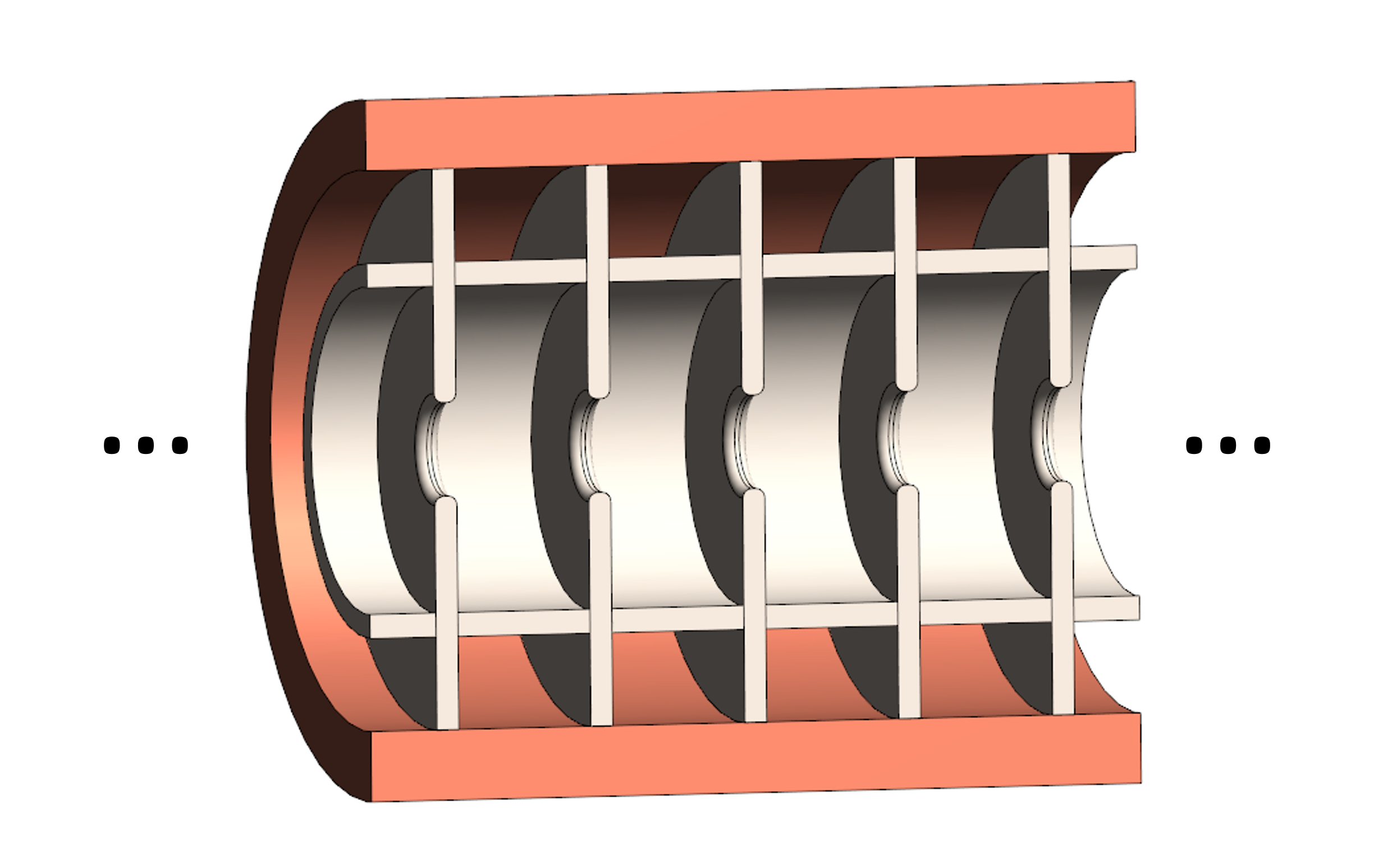
The DAA structures [38, 41] consist of axially symmetric dielectric cylinders with irises periodically arranged in a metallic enclosure operating in standing wave -mode, as illustrated in Fig. 1.
II-A Regular cell design
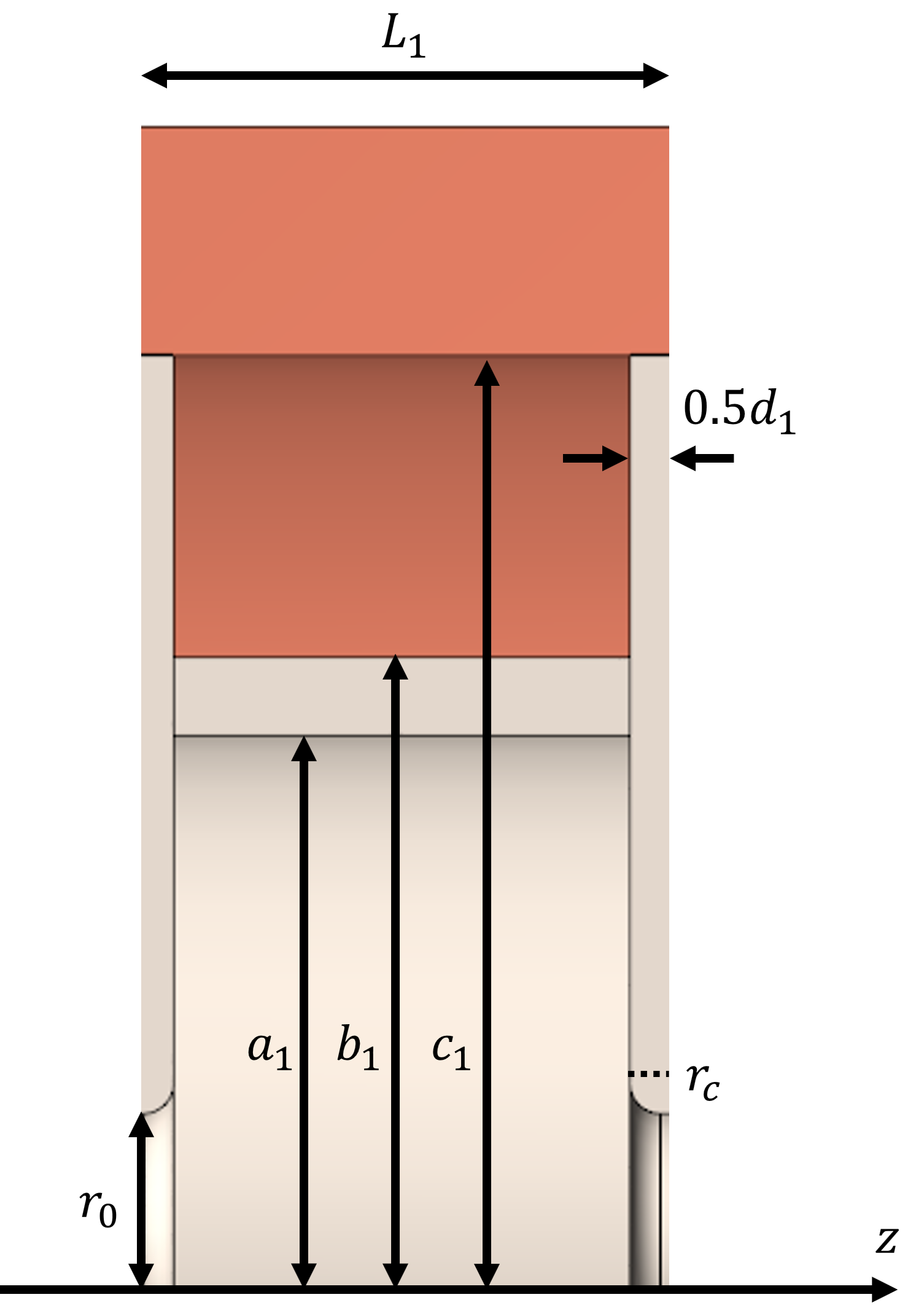
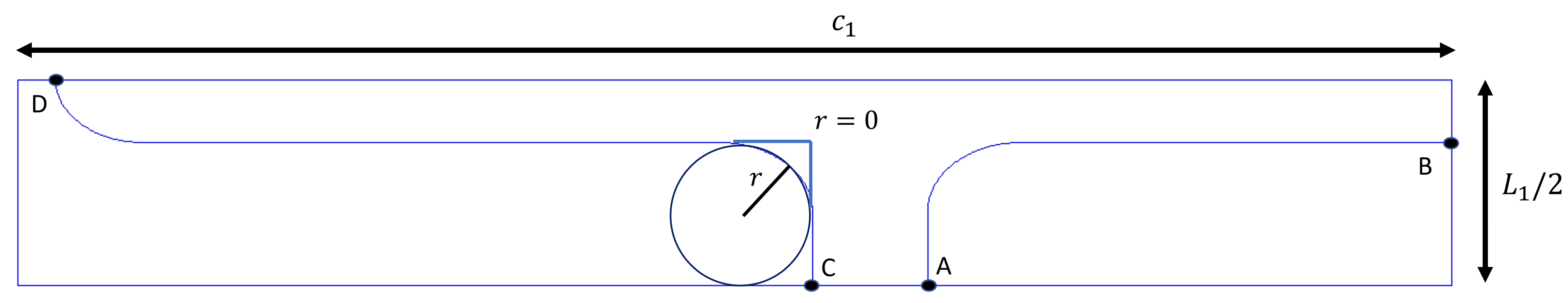
DAA design starts by optimizing parameters for the regular cell in order to maximize the and the for the resonant frequency of interest. The longitudinal cross section of the regular cell can be seen in Fig. 2, where is the aperture radius, is the corner filet radius, is the inner radius, is the outer radius, is the copper waveguide radius, is the dielectric disk thickness, also known as iris, and is the constant periodic length.
Once , and are selected based on criteria explained later, the combination of , , and determines the figures of merit in the cavity, such as resonant frequency, quality factor and shunt impedance of the accelerating mode TM02-. Thus, in this paper a new step is added to the optimization analysis, looking for the value of which, in combination with the three radius selection, maximizes the shunt impedance of the cavity, in spite of fixing this value to as was done in previous studies [38, 41]. Thanks to the axial symmetry, optimum parameters can be calculated using the SUPERFISH tool [42], in addition results have been cross checked using HFSS [43]. Periodic boundary conditions were applied to regular cell in order to simulate an infinite long structure.
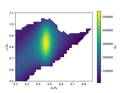
The resonant frequency goal was fixed at MHz, , where is the free space wavelength, mm for comparison with high gradient copper structures and . Then, in order to find the best values for and the radii , a two step scan needs to be done. First, is fixed at its initial value , so the resonant frequency is determined by the combination of , and . Once and are fixed, the value of can be recalculated for the given frequency using the numerical solver. Following this methodology, optimum parameters can be found by sweeping through and , finding the corresponding value of , and . This is shown in Fig. 3 for MgTiO3 with and . It must be noted here that for low electric permittivity and low particle velocity, it might be impossible to find a geometry of a regular cell with the desired resonant frequency.
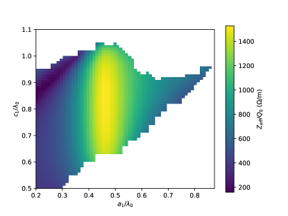
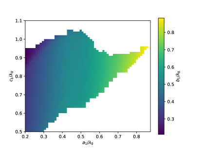
This process is repeated for each value of a second swept in , where is the normalized iris thickness. This allows to find a better solution in terms of , as illustrated in Fig. 4 for MgTiO3 with and .
The ratio of the peak electric field and the peak magnetic field to the average accelerating electric field usually limit the achievable accelerating gradient for conventional iris-loaded metallic structures, where
| (1) |
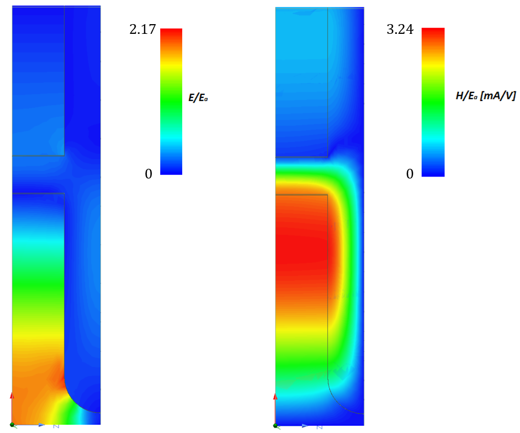
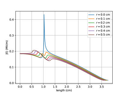
where is the longitudinal component of the electric field, is the angular frequency and is the longitudinal spatial coordinate. Field profiles for this structure are illustrated in Fig. 5.
an optimization was done using four different ceramics, whose electromagnetic properties can be found in Table I, and particles velocity . During these studies, it was observed that the geometry optimization depends mainly on the particle velocity and the relative electric permittivity of the ceramic, while loss tangent determines the final value of as well as .
| Material | Acronym | tan | |
|---|---|---|---|
| CVD Diamond | Diamond | 5.7 | |
| MgO | D9 | 9.64 | |
| MgTiO3 | D16 | 16.66 | |
| BaTiOx | D50 | 50.14 |
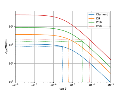
Energy ranges for Hadrontherapy treatments vary between 70-230 MeV for protons and 100-430 MeV/u for carbon ions, which correspond to particle velocities between 0.37-0.60 and 0.43-0.73, respectively [44]. Final results for the figures of merit for these designs, taking into account dielectric losses, are compared with an extension for all particle velocities of a high-gradient standing wave copper cavity designed for protons with [45], as it can be seen in Fig. 6.
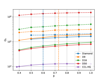
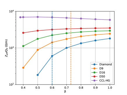
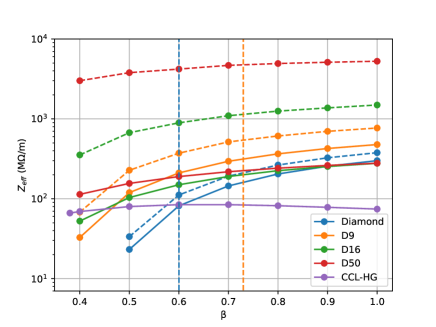
Note the difference on the performance between the ideal and relativistic case. For the ideal case, the is over two orders of magnitude higher compared to HG copper structures. As can be seen in Fig. 6, the increases with and it is very sensitive to losses in the dielectric, though results are better than normal copper cavities. One caveat of this design is that a high amount of electrical energy is stored inside the dielectric, which is not going to be used to accelerate the beam. As a consequence, energy efficiency worsens, resulting in lower values of . Energy efficiency improves for larger and, as expected, does not depend on the dielectric . The performance of the structure will be given by the shunt impedance, which is a compromise between and . For the ideal case, the final result will be better for higher . However, due to the high sensitivity of with dielectric losses, the characteristic value of of the material is crucial on the real performance of the final structure. In addition, the performance increases also for higher particle velocities.
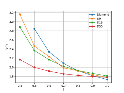
Moreover, as it is shown in Fig. 7, for the optimal geometry decreases with the material permittivity and particle velocity and it is always below 4 which is the value obtained for CCL-HG cavity [45]. This ratio is one of the main limiting factors for HG cavities, since it is related with breakdowns production. Besides, it was observed that this ratio also decreases for thinner irises. Therefore, the performance of the DAA regular cell improves with particle velocity and higher electric permittivity being able to improve current values for room-temperature copper cavities.
II-B Dielectric loss tangent
The advantage of working under the TM02- mode, is that metallic losses are highly suppressed and, consequently, the DAA regular cell performance will be determined mainly by the quality of the dielectric in terms of its .
Dielectric and metallic losses are given by [38],
| (2) |
| (3) |
respectively, where is the surface resistance, is the electric permittivity of dielectric, E is the electric field, H is the magnetic field, is the unitary normal vector to the surface, is the magnetic permeability of vacuum and S/m is the copper electric conductivity.
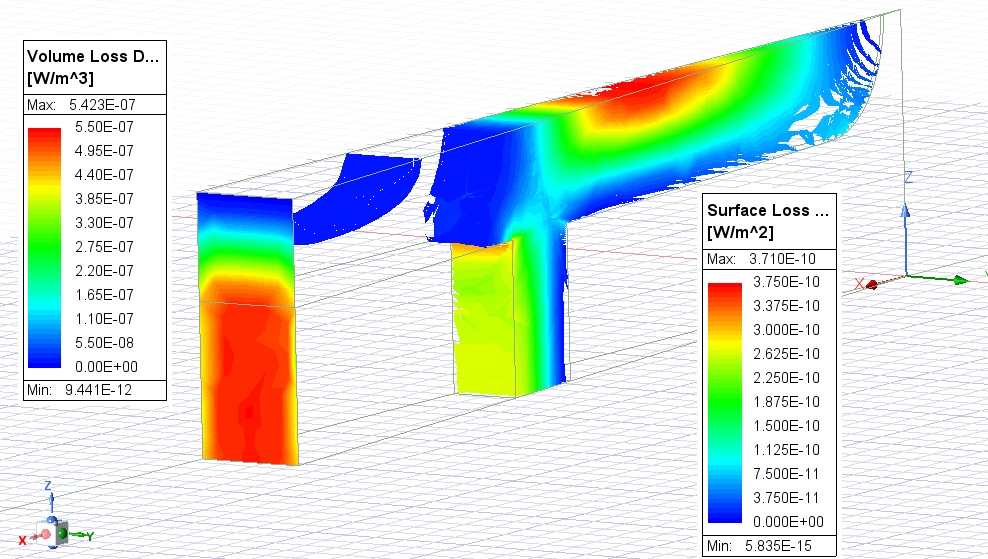
A graphical representation of both surface and volumetric loss densities are illustrated in Fig. 8. As both magnitudes have different units, a quantitatively comparison between them must be done by integrating the loss density over the whole geometry. Results are illustrated in Fig. 9, showing a strong dependence mainly on the material loss tangent.
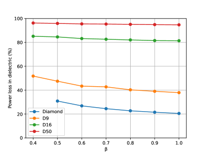
As the loss tangent depends strongly on the manufacturing process for the ceramic fabrication, values of Table I are just references from previous experimental measurements. Therefore, it is of great importance to study the dependence of regular cell performance as a function of the of the material, as illustrated in Fig. 10, where an exponential decrease of the cavity performance can be seen for values of .
III STRUCTURE PERFORMANCE
Once the optimization of the geometry has been performed, the electromagnetic performance of the regular cell has to be considered as a component of a real accelerator system. In order to do so, the dispersion relation of the regular cell is studied as well as the field instabilities and singularities which can lead to multipactor or RF breakdown discharges. Besides, the consequences of using coating to suppress multipactor in the RF performance is also deliberated.
III-A Dispersion relation
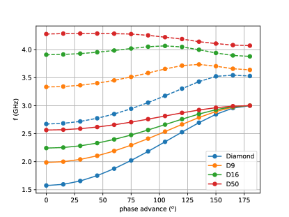
The overlapping between adjacent modes is a typical problem from the tunability and operational point of view for periodic RF accelerating structures, which is the case for the standing-wave accelerating structure studied in this work. In addition, good electromagnetic coupling between consecutive cells is also a key factor in order to determine the maximum number of cells per cavity.
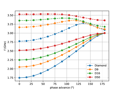
Electric coupling between consecutive cells improves for lower electric permittivity and particle velocity, as it is illustrated in Fig. 11. It can be observed that the TM02 mode is strongly electrically coupled, so there is no need for coupling cells between regular cells.
Dispersion curves for the second order mode and the next higher order mode are depicted in Fig. 12 for each material for two different normalized iris thickness. It can be seen that for low electric permittivity material, the higher order mode crosses the 3 GHz point and, therefore, overlapping cannot be avoided. In addition, as the iris becomes thicker, it can be seen that higher order modes with a phase advance of get closer to the resonant frequency and they can even cross this point for thicker irises. Consequently, electric permittivity and normalized iris thickness are bounded by the overlapping process.
III-B Field instabilities
The existence of sharp angles and triple junction points in the original design can lead to singularities in the surface electric field. As a consequence, field instabilities, RF breakdowns or multipactor discharges can emerge.
Regarding the triple junction point (point B in Fig. 13), assuming zero conductivity in dielectric and flat metal wall, the electric field increases as , where is the radial distance to the triple junction point and follows [18]:
| (4) |
where is the angle of vacuum between dielectric and metal and is the relative electric permittivity of the dielectric.
From eq. (4) it can be concluded that if º then , leading to infinitely large electric field in the junction, whereas if º then , leading to null electric field. Only the case with º leads to , implying a non-zero and non-singular value. However, we are just interested in avoiding singularities, which can be achieved by adjusting º. In addition, sharp metallic corners are another source of field singularities which must be avoided.
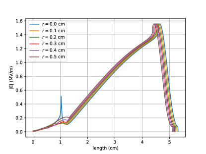
Regarding the dielectric corners in the junction between the dielectric ring and the iris, it was observed that sharp geometries also lead to field divergences. Thus, the geometry was changed as shown in Fig. 13 and the surface electric field for different round corners was studied for a fine mesh, as illustrated in Fig. 14 and Fig. 15.
III-C Coating effects
Amorphous Carbon (a-C) and Diamond Like Carbon (DLC) coatings were studied at Conseil Européen pour la Recherche Nucléaire (CERN) for Secondary Electron Yield (SEY) reduction in order to avoid multipactor discharges [46]. However, surface losses on the coating, which follow eq. (5), will have an impact on the electromagnetic performance of the cavity
| (5) |
where is the sheet surface resistance of the coating.
as a function of the sheet resistance (in ohms per ) is illustrated in Fig. 16 for different cases: no coating, dielectric fully covered with coating, internal coating (which corresponds with coating in region CD) and external coating (which corresponds with coating in region AB). The surface resistance of DLC coating was above 1 M per and could not be measured, while a-C samples measurements are marked with black dashed lines.
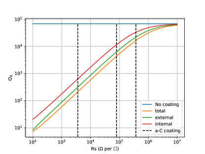
As it can be observed in Fig. 16, rapidly decreases for low resistance coatings and therefore thin films or materials with high resistivity are useful coatings to improve the electromagnetic performance.
III-D Thermal simulations
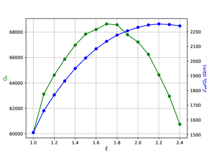
In order to estimate the required cooling system and the mechanical stress and deformation induced by RF losses, thermal simulations were carried out using the ANSYS software [47]. Volumetric and surface losses were used as input for steady thermal simulations with 3 cm of copper wall fixing the external temperature at 22ºC as boundary condition. Simulations were done for different geometries and ceramics, as illustrated in Table II. Ultra high pure alumina was used for simulations instead of MgO because of its higher thermal conductivity in order to evaluate three different meaningful values.
| Material | tan | W·m-1·K-1 | |
|---|---|---|---|
| CVD Diamond | 5.7 | 2000 | |
| Al2O3 99.99% | 9.8 | 30 | |
| MgTiO3 | 16.66 | 3.8 |
For numerical simulations, an accelerating gradient of 50 MV/m was used, with a duty cycle ,
| (6) |
where is the pulse width and is the total period of the signal. A graphical solution for Al2O3 for is shown in Fig. 17.
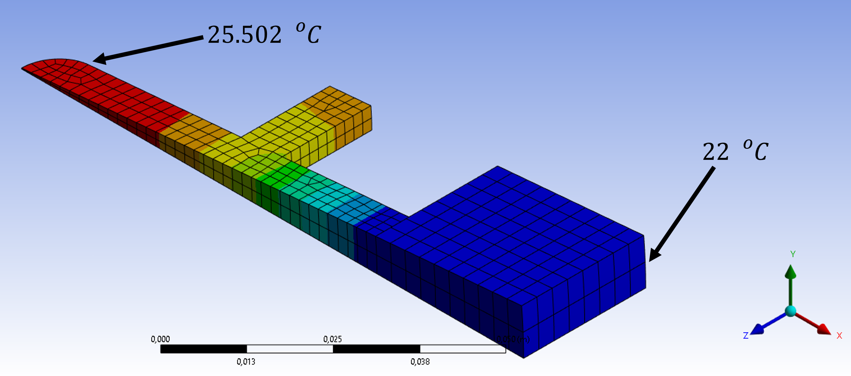
As shown in Fig. 17, the maximum temperature is reached close to the aperture of the ceramic, with a decreasing temperature gradient towards the copper metallic enclosure, which barely changes thanks to its high thermal conductivity ( W·m-1·K-1). The maximum temperature reached for different geometries and materials is illustrated in Fig. 18.
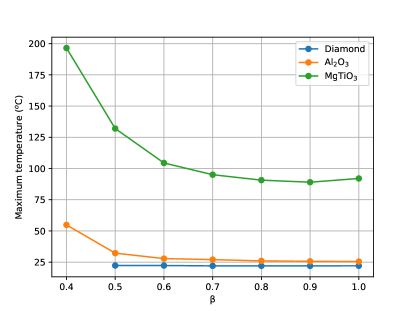
The temperature is higher for lower particle velocity while it seems to saturate at around following the behaviour of the . In addition, very low thermal conductivity, as in MgTiO3, leads to temperatures beyond acceptable limits regarding stress and deformation tolerances, even though we are still far from the fusion point.
IV Conclusion and future work
DAA structures for low particles have been studied for the first time, proving the potential to improve the performance of current room-temperature copper cavities. This study shows improvements in the optimization process and optimal results for an S-band DAA cavity as a solution for compact linear accelerators for Hadrontherapy treatments.
Working under the TM02- mode, copper ohmic losses can be highly reduced by accumulating electrical energy inside the dielectric. From these studies we could conclude that cavity efficiency increases for higher particle velocity and electric permittivity. However, due to the high energy density inside the dielectric, the cavity performance will be limited by dielectric losses. Therefore, reaching low dielectric loss tangent is a fundamental key in the fabrication of ceramics in particular for DAA cavities.
Iris thickness plays also a fundamental role in the cell optimization by increasing the accelerating voltage and also by reducing the electric energy density inside the ceramic by decreasing dielectric losses. As a consequence, materials with higher loss tangent have thicker optimum irises than ideal geometries.
In addition, the ratio is lower than those reached by copper cavities, which potentially allows DAA cavities to reach higher gradients without producing RF breakdowns. This ratio decreases for high particle velocity, high electric permittivity and thin irises.
High electric coupling between consecutive cells has been observed for all kind of geometries. In addition, it was shown that coupling improves for lower particle velocity and lower electric permittivity. However low electric permittivity materials, such as CVD diamond, suffer from mode overlapping. In addition, thicker irises produce the excitation of more modes whose resonant frequencies are close to our operational frequency. As a result, the final design must find a compromise between an optimum electromagnetic design, which is achieved for thicker irises and low mode overlapping and low peak electric field, which improve for thinner irises.
Dielectric corners have been rounded in order to smooth the surface electric field. Moreover, stability studies of triple junction point were performed concluding that in order to avoid electric field singularities, the vacuum angle between dielectric and copper must be º and metallic sharp angles must be avoided.
Multipactor is one of the main limitations of DLA cavities due to high SEY of ceramics. Because of that, thin coating with low SEY is used for multipactor suppression. However, surface resistance of coating will have an effect on RF performance that must be studied in advance. Numerical simulations showed that low resistance coatings are unacceptable from an electromagnetic point of view, which implies that only high resistance materials or very thin coatings can be used in order to reduce multipactor.
Finally, thermal conductivity of the ceramic is found to be a crucial parameter also on the design to avoid overheating of the cavity leading to high deformation and stress. Thus, a lower bound value is set around 20-30 W·m-1·K-1 depending on particle velocity and duty cycle.
Acknowledgment
Work supported by Ministerio de Universidades (Gobierno de España) under grant number FPU19/00585 and EST22/00739.
References
- [1] T. Shintake, H. Tanaka, T. Hara, T. Tanaka, K. Togawa, M. Yabashi, Y. Otake, Y. Asano, T. Bizen, T. Fukui et al., “A compact free-electron laser for generating coherent radiation in the extreme ultraviolet region,” Nature Photonics, vol. 2, no. 9, pp. 555–559, 2008.
- [2] E. Tanabe, Y. Fineberg, H. Matsumoto, and T. Shintake, “Medical applications of c-band accelerator technologies,” in Proc. Linear Accel. Conf, 1998, pp. 627–629.
- [3] R. Sethi et al., “Electron beam accelerators for materials processing: A barc scenatrio,” in Proc. of APAC, 2004, pp. 708–710.
- [4] M. Aicheler, P. Burrows, M. Draper, T. Garvey, P. Lebrun, K. Peach, N. Phinney, H. Schmickler, D. Schulte, and N. Toge, “A multi-tev linear collider based on clic technology: Clic conceptual design report,” SLAC National Accelerator Lab., Menlo Park, CA (United States), Tech. Rep., 2014.
- [5] A. Degiovanni, U. Amaldi, R. Bonomi, M. Garlasché, A. Garonna, S. Verdú-Andrés, and R. Wegner, “Tera high gradient test program of rf cavities for medical linear accelerators,” Nuclear Instruments and Methods in Physics Research Section A: Accelerators, Spectrometers, Detectors and Associated Equipment, vol. 657, no. 1, pp. 55–58, 2011.
- [6] S. Benedetti, “High-gradient and high-efficiency linear accelerators for hadron therapy,” Ph.D. dissertation, Ecole Polytechnique Fédérale de Lausanne, 2018.
- [7] A. Vnuchenko, “High-gradient issues in s-band rf acceleration structure for hadrontherapy accelerators and radio frequency quadrupoles,” Ph.D. dissertation, University of Valencia, 2020.
- [8] W. Gai, R. Konecny, and J. Simpson, “Externally powered dielectric loaded waveguides as accelerating structures,” in Proceedings of the 1997 Particle Accelerator Conference (Cat. No. 97CH36167), vol. 1. IEEE, 1997, pp. 636–638.
- [9] W. Liu, C. Jing, W. Gai, R. Konecny, and J. Power, “New rf design for 11.4 ghz dielectric loaded accelerator,” in Proceedings of the 2003 Particle Accelerator Conference, vol. 3. IEEE, 2003, pp. 1810–1812.
- [10] S. Gold, C. Jing, A. Kanareykin, W. Gai, R. Konecny, W. Liu, J. Power, and A. Kinkead, “Development and testing of x-band dielectric-loaded accelerating structures,” in Proc. Part. Accel. Conf, 2010, pp. 3001–3003.
- [11] Y. Wei, A. Grudiev, B. Freemire, and C. Jing, “A compact, low-field, broadband matching section for externally powered x-band dielectric-loaded accelerating structures,” IEEE Transactions on Nuclear Science, vol. 69, no. 5, pp. 991–1001, 2022.
- [12] Y. Wei, H. Bursali, A. Grudiev, B. Freemire, C. Jing, R. Wegner, J. S. Bedolla, and C. Welsch, “Design, fabrication, and low-power rf measurement of an x-band dielectric-loaded accelerating structure,” Physical Review Accelerators and Beams, vol. 25, no. 4, p. 041301, 2022.
- [13] M. Thompson, H. Badakov, A. Cook, J. Rosenzweig, R. Tikhoplav, G. Travish, I. Blumenfeld, M. Hogan, R. Ischebeck, N. Kirby et al., “Breakdown limits on gigavolt-per-meter electron-beam-driven wakefields in dielectric structures,” Physical review letters, vol. 100, no. 21, p. 214801, 2008.
- [14] C. Jing, W. Gai, J. Power, R. Konecny, S. H. Gold, W. Liu, and A. K. Kinkead, “High-power rf tests on x-band dielectric-loaded accelerating structures,” IEEE transactions on plasma science, vol. 33, no. 4, pp. 1155–1160, 2005.
- [15] C. Jing, W. Gai, J. G. Power, R. Konecny, W. Liu, S. H. Gold, A. K. Kinkead, S. G. Tantawi, V. Dolgashev, and A. Kanareykin, “Progress toward externally powered x-band dielectric-loaded accelerating structures,” IEEE transactions on plasma science, vol. 38, no. 6, pp. 1354–1360, 2010.
- [16] C. Jing, C. Chang, S. Gold, R. Konecny, S. Antipov, P. Schoessow, A. Kanareykin, and W. Gai, “Observation of multipactor suppression in a dielectric-loaded accelerating structure using an applied axial magnetic field,” Applied Physics Letters, vol. 103, no. 21, p. 213503, 2013.
- [17] C. Jing, S. Gold, R. Fischer, and W. Gai, “Complete multipactor suppression in an x-band dielectric-loaded accelerating structure,” Applied Physics Letters, vol. 108, no. 19, p. 193501, 2016.
- [18] B. Techaumnat, S. Hamada, and T. Takuma, “Effect of conductivity in triple-junction problems,” Journal of electrostatics, vol. 56, no. 1, pp. 67–76, 2002.
- [19] B. Freemire, C. Jing, S. Poddar, E. Beamlabs, Y. Zhao, E. Techlabs, M. Conde, D. Doran, G. Ha, W. Liu et al., “High power test of a dielectric disk loaded accelerator for a two beam wakefield accelerator,” in 12th International Particle Accelerator Conference (IPAC’21), Campinas, SP, Brazil, 24-28 May 2021. JACOW Publishing, Geneva, Switzerland, 2021, pp. 1096–1099.
- [20] S. Frankel, “Tm 0, 1 mode in circular wave guides with two coaxial dielectrics,” Journal of Applied Physics, vol. 18, no. 7, pp. 650–655, 1947.
- [21] G. Bruck and E. Wicher, “Slow transverse magnetic waves in cylindrical guides,” Journal of Applied Physics, vol. 18, no. 8, pp. 766–769, 1947.
- [22] A. Oliner, “Remarks on slow waves in cylindrical guides,” Journal of Applied Physics, vol. 19, no. 1, pp. 109–110, 1948.
- [23] R. S. HARVIE, “A proposed new form of dielectric-loaded wave-guide for linear electron accelerators,” Nature, vol. 162, no. 4127, pp. 890–890, 1948.
- [24] G. Cohn and G. Flesher, “Design construction and initial operation of a continuous dielectric loaded linear accelerator,” Electron. Res. Laboratories, Illinois Inst. Technol. Chicago, IL, USA, Tech. Rep, vol. 2, 1952.
- [25] L. Mullett, W. Walkinshaw, J. Bell, B. Loach et al., “A theoretical and experimental investigation of anisotropic-dielectric-loaded linear electron accelerators,” Proceedings of the IEE-Part B: Radio and Electronic Engineering, vol. 104, no. 15, pp. 273–290, 1957.
- [26] G. Walker and E. Lewis, “Vacuum breakdown in dielectric-loaded wave-guides,” Nature, vol. 181, no. 4601, pp. 38–39, 1958.
- [27] R. Woode, E. Ivanov, M. Tobar, and D. Blair, “The measurement of the dielectric loss tangent of alumina at microwave frequencies and room temperature,” Electronics Letters, vol. 30, no. 25, pp. 2120–2122, 1994.
- [28] N. M. Alford and S. J. Penn, “Sintered alumina with low dielectric loss,” Journal of Applied Physics, vol. 80, no. 10, pp. 5895–5898, 1996.
- [29] C.-L. Huang, J.-J. Wang, and C.-Y. Huang, “Microwave dielectric properties of sintered alumina using nano-scaled powders of alumina and tio2,” Journal of the American Ceramic Society, vol. 90, no. 5, pp. 1487–1493, 2007.
- [30] A. Templeton, X. Wang, S. J. Penn, S. J. Webb, L. F. Cohen, and N. M. Alford, “Microwave dielectric loss of titanium oxide,” Journal of the American Ceramic Society, vol. 83, no. 1, pp. 95–100, 2000.
- [31] J. D. Breeze, X. Aupi, and N. M. Alford, “Ultralow loss polycrystalline alumina,” Applied physics letters, vol. 81, no. 26, pp. 5021–5023, 2002.
- [32] A. Kanareykin, “New advanced dielectric materials for accelerator applications,” in AIP Conference Proceedings, vol. 1299, no. 1. American Institute of Physics, 2010, pp. 286–291.
- [33] C. Jing, A. Kanareykin, S. Kazakov, W. Liu, E. Nenasheva, P. Schoessow, and W. Gai, “Development of a dual-layered dielectric-loaded accelerating structure,” Nuclear Instruments and Methods in Physics Research Section A: Accelerators, Spectrometers, Detectors and Associated Equipment, vol. 594, no. 2, pp. 132–139, 2008.
- [34] P. Zou, L. Xiao, X. Sun, W. Gai, and T. Wong, “Hybrid dielectric and iris-loaded periodic accelerating structure,” Journal of Applied Physics, vol. 90, no. 4, pp. 2017–2023, 2001.
- [35] J. Shao, C. Jing, J. Power, M. Conde, and D. Doran, “Study of a dielectric disk structure for short pulse two-beam acceleration,” Group, vol. 1, no. 10, p. 4, 2018.
- [36] J. Power, W. Gai, S. Gold, A. Kinkead, R. Konecny, C. Jing, W. Liu, and Z. Yusof, “Observation of multipactor in an alumina-based dielectric-loaded accelerating structure,” Physical review letters, vol. 92, no. 16, p. 164801, 2004.
- [37] C. Jing, A. Kanareykin, J. Power, M. Conde, Z. Yusof, and W. Gai, “Observation of enhanced transformer ratio in collinear wakefield acceleration,” in AIP Conference Proceedings, vol. 877, no. 1. American Institute of Physics, 2006, pp. 511–519.
- [38] D. Satoh, M. Yoshida, and N. Hayashizaki, “Dielectric assist accelerating structure,” Physical Review Accelerators and Beams, vol. 19, no. 1, p. 011302, 2016.
- [39] D. Satoh and H. N. Yoshida, M, “Fabrication and cold test of dielectric assist accelerating structure,” Physical Review Accelerators and Beams, vol. 20, no. 9, p. 091302, 2017.
- [40] S. Mori, M. Yoshida, and D. Satoh, “Multipactor suppression in dielectric-assist accelerating structures via diamondlike carbon coatings,” Physical Review Accelerators and Beams, vol. 24, no. 2, p. 022001, 2021.
- [41] Y. Wei and A. Grudiev, “Investigations into x-band dielectric assist accelerating structures for future linear accelerators,” IEEE Transactions on Nuclear Science, vol. 68, no. 5, pp. 1062–1071, 2021.
- [42] K. Halbach and R. F. Holsiger, “Superfish - a computer program for evaluation of rf cavities with cylindrical symmetry,” Particle Accelerators,, vol. 7, pp. 213–222, 1976.
- [43] ANSYS HFSS software. [Online]. Available: http://www.ansoft.com/products/hf/hfss/
- [44] V. Bencini, “Design of a novel linear accelerator for carbon ion therapy,” Ph.D. dissertation, Rome U., 2020.
- [45] S. Benedetti, A. Grudiev, and A. Latina, “High gradient linac for proton therapy,” Physical Review Accelerators and Beams, vol. 20, no. 4, p. 040101, 2017.
- [46] A. Grudiev, S. Poddar, H. Neupert, W. Vollenberg, B. Freemire, and C. Jing, “Amorphous and diamond-like carbon coatings for sey reduction of dielectric materials for accelerating structure applications,” Tech. Rep., 2022.
- [47] ANSYS software. [Online]. Available: https://www.ansys.com/