Structural properties of epitaxial -U thin films on Ti, Zr, W and Nb
Abstract
Thin layers of orthorhombic uranium (-U) have been grown onto buffered sapphire substrates by d.c. magnetron sputtering, resulting in the discovery of new epitaxial matches to Ti(00.1) and Zr(00.1) surfaces. These systems have been characterised by X-ray diffraction and reflectivity and the optimal deposition temperatures have been determined. More advanced structural characterisation of the known Nb(110) and W(110) buffered -U systems has also been carried out, showing that past reports of the domain structures of the U layers are incomplete. The ability of this low symmetry structure to form crystalline matches across a range of crystallographic templates highlights the complexity of U metal epitaxy and points naturally toward studies of the low temperature electronic properties of -U as a function of epitaxial strain.
I Introduction
Many of the actinides and their compounds exhibit fascinating condensed matter physics, including a plethora of unusual structural and electronic ground states (e.g. complex polymorphism, unconventional magnetic ordering and heavy fermion superconductivity). These properties often arise as a result of the outer-shell 5 electrons being situated on the boundary between itinerancy and localisation [1, 2, 3, 4, 5]. The mid-series actinide metals (U, Np, Pu) exemplify these characteristics, with each of the three distinct crystallographic structures adopted by bulk U exhibiting notable collective electronic phenomena at low temperatures [6, 7].
The thermodynamically stable phase of uranium under ambient conditions is orthorhombic -U (). This phase is unique amongst the elements, both for its low symmetry crystal structure and for its unusual electronic properties, with bulk -U crystals undergoing a series of three charge density wave (CDW) transitions before entering a superconducting (SC) state. Although the superconducting transition temperature () appears to vary unpredictably with sample crystallinity and purity ( K), it is generally accepted that isotropic compressive pressure can be used to suppress the CDW transitions and enhance to a maximum of 2 K near 1.5 GPa [8, 9, 10]. The exact nature of the interaction between the SC and CDW states in -U is yet to be understood, but a combination of bulk and thin film studies have since confirmed that pressure-induced changes to the low temperature states are related primarily to the length of the -axis [11, 12].
Epitaxial strain engineering can often be used to explore regions of phase space that are inaccessible in bulk experiments involving uranium. For example, epitaxial layers of -U with host an incommensurate ‘bulk-like’ CDW below 43 K, while U layers with (i.e. a strain that would be difficult to attain in bulk crystals) host a near-commensurate CDW with an increased onset temperature of 120 K [13, 12]. Compression of the -axis and expansion of the -axis are both predicted to stabilise the CDW state in -U [14], but the influence of uniaxial strain along these axes has not yet been explored.
| Substrate | Buffer | (∘C) | (Å) | (∘C) | (Å) | Cap | (Å) |
|---|---|---|---|---|---|---|---|
| Al2O3(11.0) | Nb(110) | 800 | 200 | 600 | 5000 | Nb | 130 |
| Al2O3(11.0) | W(110) | 750 | 85 | 450 | 1000 | W | 90 |
| Al2O3(00.1) | Zr(00.1) | 700 | 220 | 20, 250, 400, 500 | 520 | Nb | 150 |
| Al2O3(00.1) | Ti(00.1) | 600 | 180 | 20, 200, 400, 600 | 600 | Ir or Ti | 85 or 180 |
It is also known that deposition onto other crystallographic templates can produce well-ordered overlayers that are difficult to stabilise in the bulk. Recently, crystalline layers of the tetragonal -U phase have been stabilised at room temperature via deposition onto Si(111) [15] and single crystal layers of a pseudo body-centred cubic -U structure have been realised by the co-deposition of U and Mo onto Nb(110) [16]. Uranium may also form a ‘hexagonal close-packed’ (hcp) structure that is not found in the bulk when deposited on W(110) [17, 18, 19], Gd(00.1) [13, 20] and Cu(111) or Ir(111) buffer layers, although the U layers in the final two systems gradually transition back into -U [21].
Given the rich array of nearly degenerate structural ground states, it is often difficult to predict the phase and orientation that a uranium layer will form under specific growth conditions. A key task in this area is, therefore, to examine a range of metallic buffer layers that can be used to stabilise high quality epitaxial layers of each U allotrope. The range of strains, structures and orientations will allow further exploration of their intriguing electronic properties, provided the complex crystallographic domain structures are also fully characterised. In this work we investigate the epitaxy of -U onto two new buffer layers (Ti, Zr) and revisit the Nb and W systems from Ref. [22] to add new information to the previously reported domain structures.
Section II of this paper describes the growth and characterisation procedures for each thin film system. Section III explores the structure and orientation of crystalline -U grown onto Ti, Zr and W buffers as discerned from laboratory-based X-ray diffraction (XRD) and X-ray reflectivity (XRR). The epitaxy and interface quality in the Ti/U and Zr/U systems are explored as a function of temperature using these techniques. Also included in Section III are synchrotron X-ray diffraction measurements of epitaxial Nb/-U(110) systems which reveal a which reveal a previous unreported domain. The physical origin of the domain is discussed.
II Experimental Methods
II.1 Growth of epitaxial films
All samples in this study were grown using the actinide d.c. magnetron sputtering system at the University of Bristol, UK. This ultra-high vacuum system operates at base pressures of the order mbar and contains four sputtering guns inside a load-locked chamber [23]. Substrates are loaded onto an adjustable height stage adjacent to a resistive heater capable of achieving temperatures of up to 850 ∘C. The substrates for epitaxial Ti(00.1) and Zr(00.1) growth were -plane Al2O3(00.1) and the substrates for Nb(110) and W(110) growth were -plane Al2O3(11.0). All substrates (sourced from MTI Corp) were polished to optical grade.
The nominal layer thicknesses and growth temperatures are given in Table 1. The buffer growth temperature is denoted as and the uranium growth temperature as with respective film thicknesses, and . Each sample was capped with a layer of a corrosion resistant metal deposited at room temperature in order to protect the U from ex-situ oxidation. All layers were deposited using approximately 10-3 mbar high purity argon gas as the sputtering medium.
II.2 Structural characterisation
Structural characterisation of the Ti/U, Zr/U and W/U systems was performed using a Philips X’Pert diffractometer with a Cu-Kα source. XRR profiles were modelled using the GenX package, where the error bars on each fitting parameter are calculated from a 5% change in the optimal figure of merit [24]. Characterisation of the Nb/U system was performed using the diffuse scattering diffractometer at the ID28 beamline (ESRF, France) [25]. Synchrotron data were treated using the CrysAlis Pro software package [26], high resolution reciprocal space maps were produced using in-house programs and visualised in the DECTRIS Albula package [27]. All X-ray measurements were conducted at room temperature.
III Results and discussion
III.1 Titanium buffered system
Titanium was sputtered onto Al2O3(00.1) substrates at 600 ∘C to produce epitaxial hexagonal close-packed Ti(00.1) layers with the in-plane relationship and thickness 180 Å. Uranium layers with a nominal thickness of Å were subsequently deposited at various temperatures. Fig. 1 shows the coupled - scans and rocking curves from the temperature series. XRR profiles with discernible Kiessig fringes are included as Supplemental Information [28]. Table 2 summarises the spacings, widths of each rocking curve () and the XRR-derived root-mean-square roughnesses () across the series.
| (∘C) | (Å) | (∘) | (Å3) | (Å) |
|---|---|---|---|---|
| 20 | 2.578 | 0.933 | 21.207 | |
| 200 | 2.568 | 0.455 | 20.885 | |
| 400 | 2.565 | 0.370 | - | - |
| 600 | 2.564 | 0.543 | - | - |
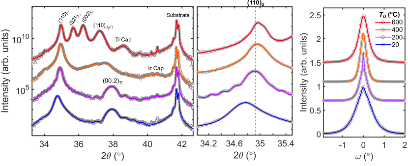
At the two lowest tested deposition temperatures, the U layer forms crystalline -U(110). At ∘C, the out-of-plane spacing ( Å) is 0.44% larger than bulk ( Å) and the peak asymmetry suggests a strain gradient from smaller to larger spacings across the vertical extent of the film. Least-squares refinement from the positions of multiple off-specular reflections gives Å (+0.26%), Å (+1.34%), Å (+0.67%) and an atomic cell volume of Å3 (+2.3%), where all percentages given are relative to bulk U at room temperature from Ref. [29].
At ∘C, the specular -U(110) peak is instead symmetric and close to the bulk value, with lattice parameters of Å (+0.14%), Å (-0.25%), Å (+0.76%) and an atomic volume of Å3 (+0.65%) indicating that the -axis strain has changed from tensile to compressive while the -axis expansion persists. The Laue fringes are suggestive of high crystallinity and a sharp U-Ti interface. The periodicity of the oscillations can be used to extract the crystalline ordered volume, with the agreement between Å and the XRR derived thickness of 6 Å suggesting that crystalline order is maintained throughout the full thickness of the U layer. The rocking curve also adopts the distinctive two-component lineshape common to many high quality thin films [30, 31].
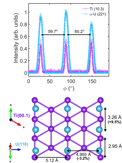
The in-plane epitaxial relationships in these two well-ordered systems were determined from the in-plane () dependence of the Ti(10.3) and U(221) off-specular reflections. The example dataset shown in the top panel of Fig. 2 indicates an approximate alignment of
The epitaxy is likely to be governed by the match shown in the bottom panel of Fig. 2 where the misfit strain, ( at room temperature is %. As hcp-Ti is six-fold symmetric in the (00.1) plane, any 60 () in-plane rotation of the U layer brings the relevant planes into alignment. This should result in six energetically equivalent ways for the first monolayer of uranium to nucleate on the Ti(00.1) surface, as confirmed by the 60∘ separation of the (114) peaks in the -scan.
The stability of epitaxial -U at these relatively low deposition temperatures was unexpected, as epitaxial Nb(110)/-U(110) and W(110)/-U(001) systems are typically grown at 450-600 ∘C [22, 13, 12]. In the case of Ti/U, temperatures above 200∘C are clearly detrimental to the quality of the interface. The degradation of the XRR signal, rocking curve profile and U/Ti Laue fringes all suggest that the sharp U-Ti interface, and hence the coherent epitaxial match, has been partially lost at C and fully lost at C. The additional, non-elemental diffraction peaks seen in the - scans are likely to originate from Ti-rich alloys () and U2Ti () [32].
III.2 Zirconium buffered system
A similar series was grown using zirconium buffer layers deposited onto -plane sapphire at 700 ∘C. These single crystal Zr(00.1) layers adopt an in-plane epitaxial relationship of Al2O3[10.0]Zr[10.0] and exhibit rocking curves with widths of 1-2∘. This limits the mosaic spread and grain size of subsequent U layers, but the epitaxial relationships are still of interest. Fig. 3 shows the coupled - scans for the series.
At room temperature, the spectrum is primarily -U(110) with small inclusions of -U(001). The off-specular reflections, included as Supplemental Information [28], suggest an orientation relationship of
where the alignment of Å and Å produces a low misfit strain of -0.6 %. As with the Ti/-U(110) system, the hexagonal symmetry of the buffer facilitates six equivalent matches in 360∘. The measured -U lattice parameters are Å (-0.015%), Å (-0.73%) and Å (+3.6%) and the atomic volume of Å3 (+3.1%) is unusually large, even for a structure as malleable as -U.
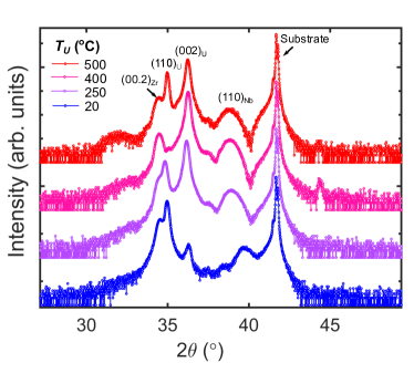
As the deposition temperature is increased toward 400∘C, the sample gradually becomes pure -U(001), with the (002) reflection gaining relatively weak Laue fringes. The orientation relationship between the layers determined from the Zr(10.5) and -U(023) reflections (Fig. S3 in Supplemental Information [28]) is
where the alignment of Å and Å results in a large misfit strain of +4.6 %. The refined lattice parameters are Å (+0.39 %), Å (-0.71 %), Å (-0.05 %) and the atomic volume is bulk-like at Å3. Again, six-fold symmetry is seen in the -U(023) -scan due to the six equivalent matches with the hexagonal Zr(00.1) surface.
The transition from an -U(110) layer with a low strain epitaxial match and a large atomic volume, to an -U(001) layer with a large misfit strain and a bulk-like atomic volume suggests it is energetically favourable for the -U structure to revert to a bulk-like atomic volume at the expense of the epitaxial match and quality of the interface. The formation of a interfacial U-Zr layer that may influence the epitaxy is also suggested by the data.
A 1-2 nm reduction in with increasing is seen via the XRR-derived U layer thicknesses and, at 500 ∘C, the reflectivity profile no longer shows Kiessig fringes. A gradual reduction in the intensity of the (00.2) reflection with increasing also suggests the formation of a interfacial U-Zr layer that increases in thickness with . The strains generated by the unusually large mismatch between the Zr(00.1) and -U(001) layer (+4.6 %) may be relieved by such a transition region, facilitating the observed change in orientation and reduction in atomic volume.
III.3 Tungsten buffered systems
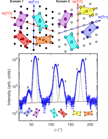
The growth of complex, multi-domain -U(001) was first reported in 2008 [22]. Ward et al. proposed a model wherein eight domains of -U nucleate on a twinned W(110) buffer as a result of a close match between the distances Å () and Å (). The two W domains and eight U domains are illustrated in the top panel of Fig. 4. In this idealised system, certain U domains (shown here in light blue and purple) are ‘degenerate’ with respect to the buffer and so a total of six peaks should be resolvable using a point detector and in-plane -scans. However, only four domains were seen in the original study [22].
The bottom panel of Fig. 4 shows a -scan of the -U(023) reflections in a new, high quality W/U sample. This scan maps the relative orientations of any (010) planes (i.e. the -axes) in the -U(001) layer. The scan shows six well-resolved peaks at angular separations that correlate well with the matches predicted by Ward et al.. A total of eight peaks are required for an accurate fit as there is a slight misorientation between the reflections from the two ‘degenerate’ (light blue and purple) pairs of domains, presumably due to strains in the buffer. These strains are also likely to be the cause of the unequal peak intensities, which imply there are strong preferences for certain U orientations. The crystalline quality of the U layer is significantly improved by reducing the deposition temperature to ∘C used in Ref. [12] as opposed to 600 ∘C used in Ref. [22].
III.4 Niobium buffered systems
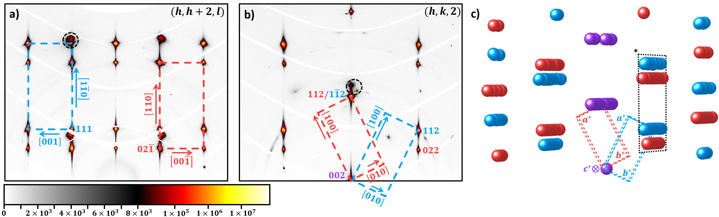
To date, all epitaxial films of -U(110) on Nb(110) have been reported as single domain systems where the epitaxy is governed by a uni-directional in-plane match between Å and Å [22, 13]. New reciprocal space maps (RSMs) taken at the ID28 beamline (ESRF) reveal a second domain consistently missed by point-detector measurements. These domains are referred to as primary ‘red’ and secondary ‘blue’ in the following discussions.
This unusual situation has arisen as the () reflections - i.e. those commonly used to check the symmetry of the U layer in laboratory -scans - are coincident, but the degeneracy is clearly lifted outside of this plane. The (,+2,) RSM in Fig. 5(a) shows an example of a fully non-degenerate plane of reflections in a Nb(110)/U system, while the (,,2) type RSM in Fig. 5(b) demonstrates both the coincidence of reflections in the () plane and splitting away from this plane. Fig. 5(c) shows the location in reciprocal space for a selection of the observed reflections, where the overlapping reflections from the two distinct domains (red and blue) are represented by purple spheres. The two -U domains are related by an approximately clockwise rotation about a shared axis set into the page, where the experimentally determined reciprocal space transformation matrix
| (1) |
transforms from primary to secondary Miller indices. The reverse operation is found by taking the inverse of the matrix in Eq. 1.
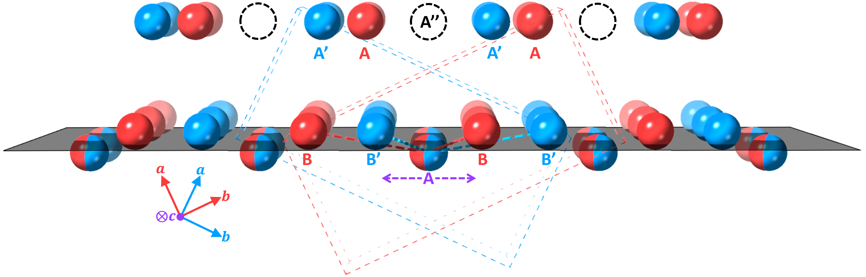
The origin of this ‘hidden’ domain can be understood as follows. As U atoms are deposited onto the Nb(110) surface, each nucleation event initiates the growth of a proto-domain of -U with a growth axis. In each of these newly forming proto-domains, the atomic arrangements in the growth plane (i.e. the lowest layer in Fig. 6) can be considered identical. However, atoms in the subsequent monolayer have an energetically degenerate choice of bonding with the long bond on the left (and short bond on the right) or the reverse, creating either a left-skewed (B) or right-skewed (B’) layer. This choice fully constrains the growth axis and defines the domain. It is important to note that a in-plane rotation fails to map one domain onto the other, instead stacking A/A’ directly above B/B’. The secondary domain origin must be shifted in-plane to ensure that the atomic sites are coincident in layer A.
If the growth mode is purely island-like, the presence of these left- and right-skewed domains is likely to result in a columnar domain structure with in-plane anti-phase domain boundaries. Pure layer-by-layer growth would preferentially create a layer with either left or right-skewedness, as vertical switching of the ‘skewedness’ would require the energetically unfavourable stacking of atoms almost directly above each other as shown in Fig. 6. The equal intensities of the two sets of reflections indicates equal domain occupations and the unlikelihood of direct atomic stacking suggests an island-like or mixed-type growth mode, but a fully conclusive determination of the atomic stacking pattern across the domain boundaries requires the application of a non-averaged technique, e.g. atomic resolution transmission electron microscopy.
It is important to acknowledge that this ‘hidden’ domain should also be present in the Ti(00.1)/-U(110) and Zr(00.1)/-U(110) systems from previous sections. Indeed, these twin domains have been observed in (241) -scans for both systems, but the scans have been omitted from this report due to their complexity. The true number of domains is then double the value suggested by the symmetry of the () -scans.
IV Conclusions
Several epitaxial -U systems have been stabilised using both new (Ti, Zr) and known (Nb, W) elemental metallic buffer layers, with some U layers forming well-ordered systems without the need for substrate heating. The range of epitaxial strains and atomic volumes observed are expected to produce significant variations in the low temperature electronic properties. A combination of magnetotransport (e.g. Hall coefficient, resistivity and magnetoresistance) and synchrotron diffraction measurements can now be used to probe the interplay between the CDW and SC ground states in these -U thin films. Specifically, studies of the superconducting transitions in Ti, Zr and W buffered samples (where K in the buffer) should be used to probe the long-standing issue of unpredictable superconductivity in bulk -U crystals. Measurements of superconductivity in the Nb buffered systems will be more challenging ( K in bulk Nb), but in the buffer could be suppressed by reducing its thickness or adding magnetic impurities. The complex structural information determined here will be essential for the accurate analysis and understanding of future electronic transport measurements conducted using -U thin films.
Acknowledgements.
This research was supported by the Engineering and Physical Sciences Research Council (EPSRC), UK, through the Centre for Doctoral Training in Condensed Matter Physics (CDT-CMP) grant no. EP/L015544/1, and the National Nuclear User Facility for Radioactive Materials Surfaces (NNUF-FaRMS), grant no. EP/V035495/1, [33]. We also acknowledge the European Synchrotron Radiation Facility (ESRF) for provision of synchrotron radiation facilities.References
- Elgazzar et al. [2009] S. Elgazzar, J. Rusz, M. Amft, P. M. Oppeneer, and J. A. Mydosh, Hidden order in URu2Si2 originates from Fermi surface gapping induced by dynamic symmetry breaking, Nature Materials 8, 10.1038/nmat2395 (2009).
- Hayes et al. [2021] I. M. Hayes, D. S. Wei, T. Metz, J. Zhang, Y. S. Eo, S. Ran, S. R. Saha, J. Collini, N. P. Butch, D. F. Agterberg, A. Kapitulnik, and J. Paglione, Multicomponent superconducting order parameter in UTe2, Science 373, 10.1126/science.abb0272 (2021).
- Stewart [2017] G. R. Stewart, Unconventional superconductivity, Advances in Physics 66, 75 (2017).
- Joynt and Taillefer [2002] R. Joynt and L. Taillefer, The superconducting phases of UPt3, Reviews of Modern Physics 74, 10.1103/RevModPhys.74.235 (2002).
- Clark et al. [2019] D. L. Clark, D. A. Geeson, and R. Hanrahan, Plutonium Handbook, Vol. 6 (American Nuclear Society, La Grange Park, Illinois, 2019).
- Moore and Van Der Laan [2009] K. T. Moore and G. Van Der Laan, Nature of the 5f states in actinide metals, Reviews of Modern Physics 10.1103/RevModPhys.81.235 (2009).
- Lander et al. [1994] G. H. Lander, E. S. Fisher, and S. D. Bader, The solid-state properties of uranium A historical perspective and review, Advances in Physics 43, 1 (1994).
- Fowler et al. [1967] R. D. Fowler, J. D. Lindsay, R. W. White, H. H. Hill, and B. T. Matthias, Positive isotope effect on the superconducting transition temperature of -uranium, Physical Review Letters 19, 10.1103/PhysRevLett.19.892 (1967).
- O’Brien et al. [2002] J. L. O’Brien, A. R. Hamilton, R. G. Clark, C. H. Mielke, J. L. Smith, J. C. Cooley, D. G. Rickel, R. P. Starrett, D. J. Reilly, N. E. Lumpkin, R. J. Hanrahan, and W. L. Hults, Magnetic susceptibility of the normal-superconducting transition in high-purity single-crystal -uranium, Physical Review B - Condensed Matter and Materials Physics 66, 10.1103/PhysRevB.66.064523 (2002).
- Schmiedeshoff et al. [2004] G. M. Schmiedeshoff, D. Dulguerova, J. Quan, S. Touton, C. H. Mielke, A. D. Christianson, A. H. Lacerda, E. Palm, S. T. Hannahs, T. Murphy, E. C. Gay, C. C. McPheeters, D. J. Thoma, W. L. Hults, J. C. Cooley, A. M. Kelly, R. J. Hanrahan, and J. L. Smith, Magnetotransport and superconductivity of -uranium, Philosophical Magazine 84, 2001 (2004).
- Raymond et al. [2011] S. Raymond, J. Bouchet, G. H. Lander, M. Le Tacon, G. Garbarino, M. Hoesch, J. P. Rueff, M. Krisch, J. C. Lashley, R. K. Schulze, and R. C. Albers, Understanding the complex phase diagram of uranium: The role of electron-phonon coupling, Physical Review Letters 107, 10.1103/PhysRevLett.107.136401 (2011).
- Springell et al. [2014] R. Springell, R. C. C. Ward, J. Bouchet, J. Chivall, D. Wermeille, P. S. Normile, S. Langridge, S. W. Zochowski, and G. H. Lander, Malleability of uranium: Manipulating the charge-density wave in epitaxial films, Physical Review B - Condensed Matter and Materials Physics 10.1103/PhysRevB.89.245101 (2014).
- Springell et al. [2008a] R. Springell, B. Detlefs, G. H. Lander, R. C. C. Ward, R. A. Cowley, N. Ling, W. Goetze, R. Ahuja, W. Luo, and B. Johansson, Elemental engineering: Epitaxial uranium thin films, Physical Review B - Condensed Matter and Materials Physics 78, 10.1103/PhysRevB.78.193403 (2008a).
- Xie et al. [2021] L. Xie, H. Yuan, and R. Qiu, Effect of strain on charge density wave order in -U, Chinese Physics B 31 (2021).
- Yang et al. [2021] M. Yang, B. Ke, F. Zheng, T. Yi, Z. He, K. Du, L. Zhang, N. Li, L. Wang, and P. Xing, Microstructure and stability of the deposited beta-uranium films, Journal of Nuclear Materials 547, 10.1016/j.jnucmat.2021.152796 (2021).
- Chaney et al. [2021] D. Chaney, A. Castellano, A. Bosak, J. Bouchet, F. Bottin, B. Dorado, L. Paolasini, S. Rennie, C. Bell, R. Springell, and G. H. Lander, Tuneable correlated disorder in alloys, Physical Review Materials 5, 10.1103/PhysRevMaterials.5.035004 (2021).
- Molodtsov and Boysen [1998] S. Molodtsov and J. Boysen, Dispersion of electron states: Angle-resolved photoemission on ordered films of U metal, Physical Review B - Condensed Matter and Materials Physics 57, 10.1103/PhysRevB.57.13241 (1998).
- Boysen et al. [1998] J. Boysen, P. Segovia, S. L. Molodtsov, W. Schneider, A. Ionov, M. Richter, and C. Laubschat, Dispersion of f states in U-metal and CeRh3, Journal of Alloys and Compounds 275, 493 (1998).
- Chen et al. [2019] Q. Chen, S. Tan, W. Feng, L. Luo, X. Zhu, and X. Lai, Direct observation of the f-c hybridization in the ordered uranium films on W(110), Chinese Physics B 28, 10.1088/1674-1056/28/7/077404 (2019).
- Springell et al. [2008b] R. Springell, F. Wilhelm, A. Rogalev, W. G. Stirling, R. C. C. Ward, M. R. Wells, S. Langridge, S. W. Zochowski, and G. H. Lander, Polarization of U 5f states in uranium multilayers, Physical Review B - Condensed Matter and Materials Physics 77, 10.1103/PhysRevB.77.064423 (2008b).
- Nicholls et al. [2022] R. Nicholls, C. Bell, R. Springell, G. H. Lander, and J. Bouchet, Structure and phase transitions of metastable hexagonal uranium thin films, Physical Review Materials 6, 103407 (2022).
- Ward et al. [2008] R. C. C. Ward, R. A. Cowley, N. Ling, W. Goetze, G. H. Lander, and W. G. Stirling, The structure of epitaxial layers of uranium, Journal of Physics Condensed Matter 20, 10.1088/0953-8984/20/13/135003 (2008).
- Springell et al. [2023] R. Springell, E. Lawrence Bright, D. A. Chaney, L. M. Harding, C. Bell, R. C. C. Ward, C. Bell and G. H. Lander, A review of uranium-based thin films, Advances in Physics https://doi.org/10.1080/00018732.2023.2230292 (2023).
- Björck and Andersson [2007] M. Björck and G. Andersson, GenX: An extensible X-ray reflectivity refinement program utilizing differential evolution, Journal of Applied Crystallography 40, 10.1107/S0021889807045086 (2007).
- Girard et al. [2019] A. Girard, T. Nguyen-Thanh, S. M. Souliou, M. Stekiel, W. Morgenroth, L. Paolasini, A. Minelli, D. Gambetti, B. Winkler, and A. Bosak, A new diffractometer for diffuse scattering studies on the ID28 beamline at the ESRF, Journal of Physics Condensed Matter 26, 272 (2019).
- Agilent Technologies [2014] Agilent Technologies, CrysAlisPro Data Collection and Processing Software for Agilent X-ray Diffractometers (2014).
- [27] DECTRIS, ALBULA, Tech. Rep. (325 Chestnut Strret, Suite 800, Philadelphia, PA 19106, USA).
- [28] See Supplemental Information at [URL] for additional XRD/XRR data from the Ti/U and Zr/U systems.
- Barrett et al. [1963] C. S. Barrett, M. H. Mueller, and R. L. Hitterman, Crystal structure variations in alpha uranium at low temperatures, Physical Review 129, 10.1103/PhysRev.129.625 (1963).
- Gibaud et al. [1993] A. Gibaud, R. A. Cowley, D. F. McMorrow, R. C. C. Ward, and M. R. Wells, High-resolution x-ray-scattering study of the structure of niobium thin films on sapphire, Physical Review B 48, 10.1103/PhysRevB.48.14463 (1993).
- Durand et al. [2011] O. Durand, A. Letoublon, D. J. Rogers, and F. Hosseini Teherani, Interpretation of the two-components observed in high resolution X-ray diffraction scan peaks for mosaic ZnO thin films grown on c-sapphire substrates using pulsed laser deposition, Thin Solid Films 519, 10.1016/j.tsf.2011.04.036 (2011).
- Knapton [1954] A. G. Knapton, The crystal structure of TiU2, Acta Crystallographica 7, 10.1107/s0365110x54001405 (1954).
- [33] https://nnuf-farms.bristol.ac.uk/.