Excitons in layered metal halide perovskites: an effective mass description of polaronic, dielectric and quantum confinement effects
Abstract
A theoretical model for excitons confined in layered metal halide perovskites is presented. The model accounts for polaronic effects, dielectric and quantum confinement by means of effective mass theory, image charges and Haken potentials. We use it to describe the band edge exciton of MAPbI3 structures surrounded by organic ligands. It is shown that the quasi-2D quantum and dielectric confinement of layered perovskites squeezes the exciton radius, and this in turn enhances polaronic effects as compared to 3D structures. The strong polaronic effects boost the binding energies and radiative recombination probabilities, which allows one to match experimental data in related systems. The thickness dependence of Coulomb polarization and self-energy potentials is in fair agreement with sophisticated atomistic models.
I Introduction
In the last years, 2D layered hybrid (organic-inorganic) metal halide perovskites have emerged as a new class of quasi-two-dimensional materials with outstanding optical (photovoltaic, light-emitting) properties and improved moisture stability as compared to their 3D counterparts.Smith et al. (2014); Lanty et al. (2014); Tsai et al. (2016); Hu et al. (2016); Ma et al. (2016); Pedesseau et al. (2016); Liu et al. (2016); Tsai et al. (2018); Soe et al. (2018); Wang et al. (2019); Zhou et al. (2020); Li et al. (2022) The optical properties of these objects (also referred to as nanoplatelets, NPLs) are intimately connected with the electronic structure of the band edge exciton. A large number of experimental and theoretical studies have investigated how the exciton electronic structure changes with the thickness and composition of either the inorganic layers, and those of the organic ligands in between consecutive layers.Liu et al. (2016); Chakraborty and Nag (2020); Traore et al. (2018); Zhang et al. (2020a); Yin et al. (2019); Passarelli et al. (2020); Tan et al. (2019); Even et al. (2014); Smith et al. (2017); Blancon et al. (2018); Tanaka et al. (2005); Sapori et al. (2016); Ghribi et al. (2021); Bohn et al. (2018) It is now clear that the electronic structure results from an interplay between the strong quantum confinement of the inorganic layers (the ligands have large gaps and hence act as potential barriers) and the strong dielectric confinement (the ligands have typically small dielectric constant).
While the separation between quantum and dielectric confinement effects is difficult by experimental means, computational simulations allow one to visualize the impact of each factor,Chakraborty and Nag (2021) thus paving the way towards optimal engineering of optoelectronic devices based on these materials.Geng et al. (2020) A similar scenario has been found in II-VI NPLs. Here, effective mass models have proved very useful in providing intuitive interpretations of a wide variety of experimental observations. These include exciton energy and oscillator strength dependence on the composition and material thickness,Ithurria et al. (2011); Achtstein et al. (2012); Christodoulou et al. (2018); Benchamekh et al. (2014); Dabard et al. (2021) exciton binding energies,Rajadell et al. (2017); Shornikova et al. (2021); Zelewski et al. (2019); Yang and Wise (2015); Ayari et al. (2020); Macias-Pinilla et al. (2021) heterostructure details,Rajadell et al. (2017); Llusar et al. (2019); Khan et al. (2020); Dabard et al. (2022); Polovitsyn et al. (2017) absorption and emission directionalityScott et al. (2017) and non-linear optical properties.HeckmannNL; Planelles et al. (2018) It is naturally desirable to extend effective mass models to halide perovskite quasi-2D materials. Input parameters such as effective masses and dielectric constants can be inferred from atomistic simulations already present in the literature.Katan et al. (2019)
Initial studies have been already conducted in this direction.Ghribi et al. (2021) However, there is a physical factor which has not been considered to date, and yet it constitutes a differential trait with respect to II-VI NPLs. Namely, the presence of sizable polaronic effects.Baranowski and Plochocka (2020) Polaron effects entail non-negligible carrier-phonon coupling. These are significant in hybrid metal halide perovskites because of the softness of the lattice,Ferreira et al. (2018) the low phonon energiesLétoublon et al. (2016); Sendner et al. (2016); Leguy et al. (2016) and the high difference between static and high-frequency dielectric constants in these materials.Sendner et al. (2016); Anusca et al. (2017); Melissen et al. (2015); Wilson et al. (2019) All these factors lead to Frölich constants (exciton-LO phonon coupling) up to one order of magnitude greater than in II-VI materials.Baranowski and Plochocka (2020)
There has been increasing awareness of the importance of polaron effects not only in 3D bulk hybrid perovskites,Thouin et al. (2019); Wolf et al. (2017); Bao et al. (2023); Menéndez-Proupin et al. (2015) but also in 2D layered ones. They have been shown to increase exciton effective masses,Baranowski and Plochocka (2020) affect their spin dynamics,Bourelle et al. (2022); Tao et al. (2020) radiative recombination,Neutzner et al. (2018) binding energySichert et al. (2015) and even lead to self-trapping.Zhang et al. (2020b)
Because direct inclusion of polaron effects in exciton calculations is a major challenge, semi-empirical approximations have been proposed in the literature. One such case is the Haken potential.Haken (1958) By including the electron and hole polaron radii -which can be inferred from experiments and atomistic calculationsSendner et al. (2016); Zhang et al. (2020b)- as a parameter, the electron-hole Coulomb potential is rewritten as:
| (1) |
The above expression, which is explained in more detail in the next section, contains a first term () describing the standard Coulomb interaction (with full, static screening) plus a second term () which introduces the ionic screening correction, due to carrier-lattice coupling at short distances. The latter mimics the inability of the lattice to screen the interaction when the electron-hole pair is very close (below the polaron radius), thus enhancing excitonic interactions. The Haken potential (and similar potentials, such as the BajajBajaj (1974) and Pullman-BüttnerPollmann and Büttner (1977) ones) have been shown to improve the estimates of the exciton binding energy in 3D metal halide perovskites as compared to estimates neglecting polaron effects, reconciling some controversial observations in experiments.Baranowski and Plochocka (2020); Menéndez-Proupin et al. (2015)
The goal of this article is to extend the effective mass theory description of excitons in quasi-2D systems, previously developed for II-VI NPLs,Rajadell et al. (2017) for the case of hybrid metal halide perovskites. This is done by considering not only quantum and dielectric confinement, but also polaron effects -through the inclusion of Haken-like potentials-. The technical novelty lies in the conjugation of dielectric confinement and polaronic effects. The former is conveniently expressed using the image charge method for quantum well-like structures,Kumagai and Takagahara (1989) which has proved valuable in the description of II-VI NPLs with varying thickness.Benchamekh et al. (2014); Rajadell et al. (2017); Shornikova et al. (2021); Polovitsyn et al. (2017); Yang and Wise (2015) Such a method was however posed for Coulomb-law potentials, . Here we adapt it to account for the additional Yukawa-like potential present in Eq. (1), .
We derive image charge expressions for both electron-hole interaction and for the self-energy corrections. The latter result from the interactions of carriers with their own image charges. Self-energy terms, which escape from simple Keldysh potentials often used to model dielectric confinement,Blancon et al. (2018); Ayari et al. (2020) are particularly important for accurate estimates of the excitonic band gapKatan et al. (2019); Polovitsyn et al. (2017) or exciton interactions across the organic barrier separating inorganic layers.Movilla et al. (2020)
Our model is tested for the prototypical case of MAPbI3. We find remarkable agreement with the self-energy obtained from ab-initio calculationsSapori et al. (2016) for NPLs down to a single layer, by including a single phenomenological parameter related to the non-abrupt profile of the dielectric constant in the vicinity of the organic-inorganic interfaces. We also show that polaronic interactions have a prominent role in excitons confined in few-layers metal halide perovskites. This is because the strong quantum and dielectric confinement squeeze the exciton under the polaron radius. It is then possible to explain the large binding energies (200-500 meV) reported in experiments.Blancon et al. (2018)
II Theoretical Framework
Within the effective mass formalism, the exciton ground state of a quasi-2D structure subject to quantum and dielectric confinement can be obtained from:Rajadell et al. (2017)
| (2) |
where and indexes stand for electron and hole, for the momentum operator, for the effective mass of carrier and for the energy gap between the conduction and the valence band at the point. is the confining potential set by the band offset between the perovskite layers and the surrounding ligands. Because the organic character of such ligands prevents carriers from tunneling,Blancon et al. (2018) it is convenient to set inside the perovskite domain and outside. and are the self-energy and electron-hole Coulomb potentials, which can be calculated using the image-charge method for quantum wellsKumagai and Takagahara (1989) to account for dielectric mismatch effects.
Eq. (2) has been employed on different occasions to study excitons in II-VI NPLs.Rajadell et al. (2017); Shornikova et al. (2021); Polovitsyn et al. (2017); Macias-Pinilla et al. (2021) Its extension to hybrid halide perovskite materials, requires including polaronic effects, i.e. the dressing of charge carriers by the local lattice polarization resulting from the Coulomb interaction between the carrier and the ionic lattice. This can be done by modifying and with respect to their usual expressions. Below we describe the procedure to do so.
Neglecting for the time being dielectric mismatch, polaronic effects are efficiently described by the Haken potential, which in a.u. reads:Haken (1958)
| (3) |
Here, is the electron-hole distance, the fundamental charge, the static dielectric constant and the high frequency (optical) one. The term represents ionic screening of carriers. are the electron and hole polaron radii inverse: , with the longitudinal optical phonon frequency.
Eq. (II) can be viewed either as an increase of the Coulomb interaction by the reduction of the ionic screening of carriers at short distances (first line) or as if charges embedded in polar semiconductors had a two-fold interaction:
a standard screened Coulomb interaction supplemented by
a Yukawa-like interaction in a medium of effective dielectric constant
(, second line in the equation).
We adopt the second point of view in this work.
To include dielectric mismatch in , we rely on the image charge method. Usual expressions found in the literature are obtained from Coulomb interaction terms ().Jackson (2021); Kumagai and Takagahara (1989) Here we need to revisit their derivation for the Yukawa-like terms (). The Yukawa potential is not solution of the Poisson equation, that accounts for the electromagnetic interactions carried by massless photons, and that for a point source charge in vacuum reads (MKS units):
| (4) |
with the vacuum permittivity and the electrostatic potential. Rather, the carriers of the Yukawa interactions have finite mass. Then, the Poisson equation should be modified by including a mass () term as follows:Tu et al. (2004)
| (5) |
The integration of Eq. (5) yields back the Yukawa potential:
| (6) |
In a dielectric medium other than the vacuum we should replace by a dielectric constant , and for a given charge distribution we should replace by . All and all, Eq. (5) reads:
| (7) |
In order to determine the interface boundary conditions between two homogeneous materials with different dielectric constant, and taking into account the definition of the electric displacement vector , we can rewrite Eq. (7) as . Then, we consider a thin, height slab around the interface and integrate this equation,
| (8) |
By taking into account the continuity of across the boundary, we see that as the second integral approaches zero. If we additionally use the divergence theorem to transform volumetric integrals into surface ones, we find:
| (9) |
with a unit vector crossing the interace, the area of integration, and the electric
charge density on the interface. The relevant result here is that the obtained boundary condition of
coincides with the usual one for Coulomb potentials, .
We can also show that the charge density generated by the Yukawa field on a dielectrically mismatched interface is similar to that of the Coulomb one. The potential
| (10) |
yields an electric field, . Since in spherical coordinates reads
| (11) |
then,
| (12) |
and the -component of the field is:
| (13) |
The boundary conditions at the interface between this medium and a rigid (i.e., non-polaronic) one defined by a static dielectric constant are given by Eq. (9). Then,
| (14) |
Using Eq. (13) we get:
| (15) |
with .
Note that this induced charge density is identical to that generated by a standard Coulomb potential in a rigid medium, but replacing
by .
It should be noted that in the limit of zero polaron radius (), . Then, the Yukawa induced charge density is zero. In any other case, we can replace the effect that this induced charge produces by the effect of an image charge (located either in the position of the original charge or in its mirror position, i.e., always located in the opposite region to that on which it acts) of magnitude
| (16) |
which generates a Yukawa potential
instead of a Coulomb one.
In summary, except that must be multiplied by a term, the image charges are calculated as in standard rigid media. Consequently, the potential between electrons and holes in layered metal halide perovskites (considering both, dielectric confinement and polaronic contributions) can be obtained by slightly modifying the expressions provided in Ref. Kumagai and Takagahara (1989) for rigid semiconductor quantum well-like structures. The modified potential reads as follows (back in a.u.):
| (17) |
Here,
| (18) |
with the thickness of the perovskite layers, and
| (19) |
with (the static dielectric constant of the perovskite material), (ionic correction of the perovskite), and the dielectric constant of the organic ligands. The functions are given by:
| (20) | |||||
| (21) |
The self-polarization potentials of electron and hole can be obtained from eqn (17) by setting , eliminating the terms (which represent the interaction of a charge carrier with itself), and dividing by 2 as corresponds to a self-energy:Jackson (2021)
| (22) |
where now
| (23) | |||||
| (24) |
Once Eqs. (22) and (17) are plugged into Hamiltonian (2), the exciton ground state is obtained by integrating it with a variational wavefunction of the form
| (25) |
where is a normalization factor, while and are the electron and hole single particle states, which account for quantum confinement. The exponential term is an in-plane Slater correlation factor, which captures excitonic interactions. is the effective Bohr radius, which is optimized variationally by following the computational scheme described in Refs. Planelles (2017) and Rajadell et al. (2017), including the modified potentials and to include the Yukawa-type potentials. At this regard, and for the sake of computational feasibility in the calculation of , the exponential factor in the Yukawa potential is spanned as a sum of five gaussian functions, including five linear and five non-linear fitting parameters, which are optimized from the starting set provided in Ref. Stewart (1970).
A Mathematica code to carry out the above described procedure is provided in the Electronic Supporting Information for free use. The code has minimal memory requirements and can be executed in ordinary computers, providing exciton total and binding energies (sub-meV converged), effective Bohr radius and electron-hole overlap integral.
III Results and Discussion
In this section, our model is used to investigate the connection between polaronic, dielectric confinement and quantum confinement effects in quasi-2D halide perovskite layers. For illustrative purposes, we consider MAPbI3 (MA=methylammonium). Effective parameters for this material have been proposed in the literature: dielectric constants and ,Sapori et al. (2016) effective masses , , and phonon frequency ,Baranowski and Plochocka (2020) which yield polaron radii of nm and nm. Unless otherwise noted, the low polarizability of the organic environment is characterized by .Blancon et al. (2018)
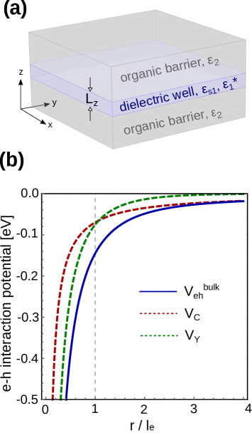
Figure 1(a) shows the different material domains of the system under study. The perovskite layers are modeled as a dielectric NPL sandwiched by organic barriers, with abrupt (step function) interfaces. The lateral dimensions of the NPL are fixed at 30x30 nm2. That is in the weak confinement (quantum-well like) regime. The number of layers defining the NPL thickness, , is a variable. Each layer is constituted by a single octahedron (unit cell) with lattice parameter nm,Ferreira et al. (2018) which add up to give a NPL thickness of .
Prior to dealing with the numerical simulations for heterostructures, it is instructive to get a qualitative view on the Haken potential in bulk MAPbI3, as it defines the basic mechanism of carrier-lattice coupling we aim to study. Figure 1(b) shows the profile of , given by Eq. (II), as a function of the electron-hole distance, in units of the electron polaron radius (blue line). Coulomb (, red line) and Yukawa (, green line) contributions are also included. As can be observed, the Yukawa term is negligible for e-h separations of the order of 4, where . However, at lower e-h distances both contributions become significant. Eventually, for , becomes more important than . In short, the smaller the exciton Bohr radius, the more relevant the ionic corrections. Major changes are expected when it approaches the polaron radius.
We shall see next that quantum and dielectric confinement greatly reduce the exciton radius in layered
perovskites with respect to their bulk value, and this indeed has a pronounced impact on its properties.
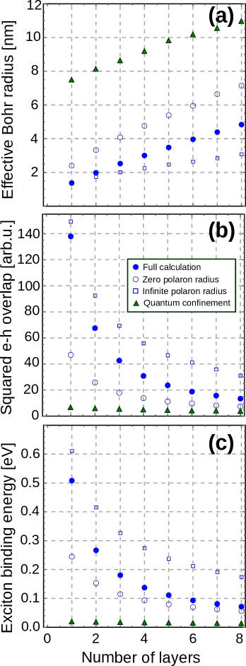
Full dots in Fig. 2(a) represent the calculated exciton Bohr radius (our variational parameter)
as a function of the number of layers conforming the NPL. For comparison, results excluding
dielectric and polaronic contributions are also shown in the figure (green triangles; is assumed).
It is clear from the trend of the triangles that the exciton radius diminishes with respect to its bulk value
when the NPL becomes thinner. This is because the vertical quantum confinement reinforces exciton interactions in the plane.Rajadell et al. (2017)
Yet, the reduction is about 4 times greater in the presence of dielectric confinement and polaronic corrections (full dots).
The overall result is a surprisingly small exciton Bohr radius, which, for low enough is
comparable to that obtained by considering infinite polaron radii (open squares in the figure),
i.e. as if .
In other words, in the few-layer limit the exciton becomes immune to the high ionic polarizability of metal halide perovskites.
Such small Bohr radii are expected to cause a sharp increase in the radiative recombination rates. The rate is proportional to the squared electron-hole overlap function, , which can be calculated analytically within our model.Rajadell et al. (2017) Fig. 2(b) confirms the rapid increase of with decreasing number of perovskite layers. This is consistent with the experimental observation of reduced photoluminescence lifetimes as the perovskite NPLs become thinner,Hintermayr et al. (2016) although a more direct comparison is hindered by the co-existence of non-radiative processes. Fig. 2(b) also shows that polaronic effects raise up to three times as compared to the case of static dielectric constant (cf full dots and empty circles). This suggests that polaronic effects in 2D layered perovskites enable faster radiative recombination than in more rigid semiconductors, such as metal chalcogenide NPLs.
Dielectric, polaronic and quantum confinement contributions also affect noticeably other exciton properties of interest, namely its binding energy . This is shown in Fig. 2(c). Because the exciton Bohr radius in a strictly 2D system is half that of the 3D case, and (with the exciton reduced mass), the relationship has been often cited in the literature to summarize the effect of quantum confinement.Chakraborty and Nag (2021); Hintermayr et al. (2016) A close inspection to the green triangles in Fig. 2(c) confirms that indeed increases as the perovksite becomes thinner by action of quantum confinement. However, the scale of the increase is greatly magnified upon inclusion of dielectric and polaronic terms (full dots). It is only in this case that the order of the binding energies ( meV) is in agreement with that measured in related structures ((BA)2(MA)n-1PbnI3n+1 perovskites with 1-5 layers, Ref. Blancon et al. (2018)).
We can disentangle dielectric and polaronic contributions in the analysis of . The impact of dielectric confinement can be measured by the difference between green triangles and open circles in the figure. The former include only quantum confinement, while the latter add dielectric confinement but no polaronic effects (static dielectric constant). It is clear that dielectric confinement alone suffices to produce a large effect on , from a 4-fold increase when to a 14-fold increase when . This can be explained as a consequence of the large polarizability of metal halide perovskites. On the one hand, the large constant of the perovskite makes the bare Coulomb contribution small. This justifies the small values of the green triangles. On the other hand, the large ratio implies a large dielectric contrast with the organic medium, which leads to enhanced surface polarization charges (or the image charges they project). These intensify the excitonic interaction, which results in much larger values of for the empty circles.
The effect of polaronic contributions can be visualized by comparing empty circles and full dots in Fig. 2(c). They become increasingly noticeable when the number of layers decreases, because becomes comparable to the polaron radius (recall Fig. 2(a)). For , the enhancement exceeds a factor of 2 (i.e. 100% increase). It is worth noting too that even for thin NPLs, the actual we calculate (full dots) have not reached the values expected in the limit of infinite polaron radius (squares). This means that relationships of the type , which are sometimes taken as reference in the literature,Chakraborty and Nag (2021) provide an upperbound estimate.
Taken together, it is remarkable that the exciton binding energies are comparable or greater to those of II-VI semiconductor
NPLs,Rajadell et al. (2017); Shornikova et al. (2021); Zelewski et al. (2019); Yang and Wise (2015); Ayari et al. (2020); Macias-Pinilla et al. (2021) despite the large polarizability of perovskites.
For , the joint effect of dielectric and polaronic contributions yields binding energies of the order of several hundreds of meV, much larger than those expected by omitting polaronic effects and in agreement with reported experimental and theoretical results.Sichert et al. (2015); Chakraborty and Nag (2021); Blancon et al. (2018); Tanaka et al. (2005)
The exciton properties presented so far are barely affected by the self-polarization potentials. However, a complete description of dielectric confinement requires their inclusion. The weak dielectric screening of the organic barriers enhances not only the e-h Coulomb interaction (), but also the interaction of carriers with their own image charges ( and ). The two effects are known to nearly compensate each other in small crystallites.Brus (1983); Bolcatto and Proetto (1999) However, in strongly anisotropic systems such as colloidal II-VI nanoplatelets, they have been shown to render sizable global effects on their emission wavelengths or composite properties.Polovitsyn et al. (2017); Movilla et al. (2020) Further evidence in this direction has been recently obtained in Cs-Pb-Br composites.Caicedo-Dávila et al. (2023) Below we show that similar effects take place in layered perovskites, and that our image charge method gives a description consistent with atomistic (DFT) simulations.
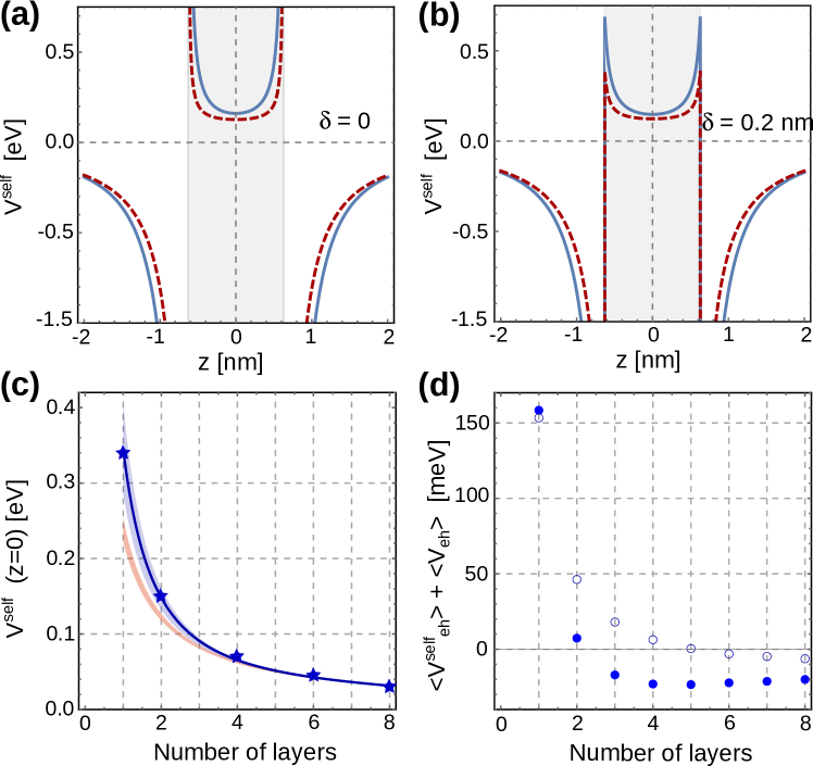
Figure 3(a) shows the -cross section of the self-polarization potential, , calculated from Eq. (22) for a 2-layer MAPbI3 system surrounded by air or vacuum (. The profile of is similar with (blue line) and without (red line) polaronic interactions. For carriers confined within the NPL, acts as a repulsive potential, which becomes attractive outside. The effect of polaronic interactions is to provide a moderate increase of the repulsions and attractions (notice the shift between lines).
On the dielectric interfaces, the potential yields non-integrable divergences. This is a well-known limitation of the image charge method when abrupt dielectric interfaces are assumed,Katan et al. (2019) arising from the coincident position of carriers and their image charge. Several strategies have been proposed to circumvent this non-physical result.Banyai et al. (1992); Bányai and Koch (1993); Bolcatto and Proetto (2001); Movilla et al. (2010) All of them rely on the argument that the notion of dielectric constant loses its meaning at distances comparable to the interatomic one, making the abrupt, stepwise dielectric profile model an oversimplification of the dielectric interface.
One strategy to sort this problem is the so-called method of the shifted mirror faces.Kumagai and Takagahara (1989) It consists in introducing a phenomenological parameter , physically related to the thickness of a finite-width interfacial layer between adjacent materials. Mathematically, the method simply replaces the terms in Eq. (22) with the following:
| (26) |
with in the range of a few Angstroms. Figure 3(b) displays the same case as in Fig. 3(a) but employing the method of the shifted mirror faces with nm. Now, the self-potential is still discontinuous, yet integrable. It is worth noting that its value influences not only at the interfaces, but also throughout all space. Then, the shift parameter turns into a fitting parameter –the only one– of this empirical model.
Because quantum confinement sets the peak of the exciton charge density in the plane of the NPL,
the value of the self-polarization potential on this plane is particularly important in determining the exciton energy,
and hence the optical band gap.
In Fig. 3(c), is represented as a function of the number of perovskite layers.
The blue-shaded region delimits the results obtained by our model for values ranging from 0 to 0.6 nm
(upper and lower limits, respectively).
For comparison, the results obtained in Ref. Sapori et al. (2016) by means of atomistic (DFT) calculations are also included (blue stars).
As can be seen, our model compares very well with the DFT results for a shift parameter of nm (blue line in the figure).
This agreement not only supports the validity of our model, but it also highlights the need to account for the non-abrupt
character of dielectric interfaces (i.e. finite ) in these materials, especially for small ,
a fact which had been independently pointed out by DFT calculations.Katan et al. (2019); Traore et al. (2018)
It is also worth stressing that the agreement with atomistic methods cannot be reached without including
polaronic () effects in the model. To make this point clear, in Fig. 3(c) we also show the self-energy
obtained for the same range of values, but taking into account contributions only (orange-shaded region).
After integrating Eq. (2) on the variational function , the exciton energy can written as:
| (27) |
where is the quantum confinement energy, the sum of electron and hole self-energy repulsions and the Coulomb attraction energy. As mentioned before, dielectric confinement enhances both and . We study the compensation between the two terms in Fig. 3(d), which is relevant in determining the total exciton energy.
Fig. 3(d) shows the totality of the electrostatic contributions
(), versus the number of layers of our MAPbI3 NPL.
Full dots (empty circles) are simulations including (excluding) polaronic terms.
In all instances, the lack of compensation between self-energy and Coulomb polarization is evident. As a matter of fact, for thin NPLs (), the energetic destabilization caused by
is greater than the stabilization caused by , such that the sum becomes positive.
This means that thin perovskite layers should experience an electrostatic blueshift in the presence of dielectric confinement,
despite the large exciton binding energy.
Polaronic interactions do not alter this trend qualitatively.
IV Concluding remarks
We have presented a model to describe exciton states in quasi-2D layered halide perovskites. The model can be used to disentangle the roles of quantum confinement (described through effective mass theory), dielectric confinement (image charge method) and polaronic effects (Haken-like potential) in these materials, which facilitates their rational design to achieve desired optoelectronic properties.
We have used the model to study layered MAPbI3 structures. The results show that polaronic effects become increasingly important as the number of layers decreases. This is because quantum and dielectric confinement reduce the exciton radius, making it similar to that of the polaron. It follows that excitons in few-layer structures are largely insensitive to the ionic polarization of the lattice, their response being close to that expected from the high frequency dielectric constant.
All in all, our work paves the way for the use of effective mass based models in the description of exciton properties of layered metal halide perovskites. Similar to the case of II-VI nanoplatelets, these can be expected to complement ab-initio methods with computationally affordable, yet intuitive and reliable descriptions of the optoelectronic properties. Such a possibility can be particularly helpful in the field of hybrid metal halide perovskite nanostructures, where atomistic simulations of excitons become extremely demanding, due to the large unit cells of these materials, the strong spin-orbit interaction (Pb), lack of translational symmetry, varying orientation of organic countercations, and the requirement of accounting for strong e-h correlations (e.g. through Bethe-Salpeter method).Chakraborty and Nag (2021)
Computational codes associated with our model are provided along with this work (ESI), and can be readily used to investigate excitons in layered perovskites built of different materials, by simply providing input bulk effective masses, dielectric constants and LO phonon frequency, which are often found in the literature, along with the dimensions of the structure.
Acknowledgements.
We acknowledge support from Grant No. PID2021-128659NB-I00, funded by Ministerio de Ciencia e Innovación (MCIN/AEI/10.13039/501100011033 and ERDF A way of making Europe) and Generalitat Valenciana Prometeo Project No. 22I235-CIPROM/2021/078.References
- Smith et al. (2014) I. C. Smith, E. T. Hoke, D. Solis-Ibarra, M. D. McGehee, and H. I. Karunadasa, A layered hybrid perovskite solar-cell absorber with enhanced moisture stability, Angewandte Chemie International Edition 53, 11232 (2014).
- Lanty et al. (2014) G. Lanty, K. Jemli, Y. Wei, J. Leymarie, J. Even, J.-S. Lauret, and E. Deleporte, Room-temperature optical tunability and inhomogeneous broadening in 2d-layered organic–inorganic perovskite pseudobinary alloys, The Journal of Physical Chemistry Letters 5, 3958 (2014).
- Tsai et al. (2016) H. Tsai, W. Nie, J.-C. Blancon, C. C. Stoumpos, R. Asadpour, B. Harutyunyan, A. J. Neukirch, R. Verduzco, J. J. Crochet, S. Tretiak, et al., High-efficiency two-dimensional ruddlesden–popper perovskite solar cells, Nature 536, 312 (2016).
- Hu et al. (2016) T. Hu, M. D. Smith, E. R. Dohner, M.-J. Sher, X. Wu, M. T. Trinh, A. Fisher, J. Corbett, X.-Y. Zhu, H. I. Karunadasa, et al., Mechanism for broadband white-light emission from two-dimensional (110) hybrid perovskites, The Journal of Physical Chemistry Letters 7, 2258 (2016).
- Ma et al. (2016) C. Ma, C. Leng, Y. Ji, X. Wei, K. Sun, L. Tang, J. Yang, W. Luo, C. Li, Y. Deng, et al., 2d/3d perovskite hybrids as moisture-tolerant and efficient light absorbers for solar cells, Nanoscale 8, 18309 (2016).
- Pedesseau et al. (2016) L. Pedesseau, D. Sapori, B. Traore, R. Robles, H.-H. Fang, M. A. Loi, H. Tsai, W. Nie, J.-C. Blancon, A. Neukirch, et al., Advances and promises of layered halide hybrid perovskite semiconductors, ACS nano 10, 9776 (2016).
- Liu et al. (2016) J. Liu, Y. Xue, Z. Wang, Z.-Q. Xu, C. Zheng, B. Weber, J. Song, Y. Wang, Y. Lu, Y. Zhang, et al., Two-dimensional ch3nh3pbi3 perovskite: synthesis and optoelectronic application, ACS nano 10, 3536 (2016).
- Tsai et al. (2018) H. Tsai, W. Nie, J.-C. Blancon, C. C. Stoumpos, C. M. M. Soe, J. Yoo, J. Crochet, S. Tretiak, J. Even, A. Sadhanala, et al., Stable light-emitting diodes using phase-pure ruddlesden–popper layered perovskites, Advanced materials 30, 1704217 (2018).
- Soe et al. (2018) C. M. M. Soe, W. Nie, C. C. Stoumpos, H. Tsai, J.-C. Blancon, F. Liu, J. Even, T. J. Marks, A. D. Mohite, and M. G. Kanatzidis, Understanding film formation morphology and orientation in high member 2d ruddlesden–popper perovskites for high-efficiency solar cells, Advanced Energy Materials 8, 1700979 (2018).
- Wang et al. (2019) J. Wang, Y. Mi, X. Gao, J. Li, J. Li, S. Lan, C. Fang, H. Shen, X. Wen, R. Chen, et al., Giant nonlinear optical response in 2d perovskite heterostructures, Advanced Optical Materials 7, 1900398 (2019).
- Zhou et al. (2020) G. Zhou, Y. Xu, and Z. Xia, Perovskite multiple quantum wells on layered materials toward narrow-band green emission for backlight display applications, ACS applied materials & interfaces 12, 27386 (2020).
- Li et al. (2022) Y.-T. Li, L. Han, H. Liu, K. Sun, D. Luo, X.-L. Guo, D.-L. Yu, and T.-L. Ren, Review on organic–inorganic two-dimensional perovskite-based optoelectronic devices, ACS Applied Electronic Materials 4, 547 (2022).
- Chakraborty and Nag (2020) R. Chakraborty and A. Nag, Correlation of dielectric confinement and excitonic binding energy in 2d layered hybrid perovskites using temperature dependent photoluminescence, The Journal of Physical Chemistry C 124, 16177 (2020).
- Traore et al. (2018) B. Traore, L. Pedesseau, L. Assam, X. Che, J.-C. Blancon, H. Tsai, W. Nie, C. C. Stoumpos, M. G. Kanatzidis, S. Tretiak, et al., Composite nature of layered hybrid perovskites: assessment on quantum and dielectric confinements and band alignment, ACS nano 12, 3321 (2018).
- Zhang et al. (2020a) L. Zhang, X. Zhang, and G. Lu, Intramolecular band alignment and spin–orbit coupling in two-dimensional halide perovskites, The Journal of Physical Chemistry Letters 11, 6982 (2020a).
- Yin et al. (2019) J. Yin, P. Maity, R. Naphade, B. Cheng, J.-H. He, O. M. Bakr, J.-L. Brédas, and O. F. Mohammed, Tuning hot carrier cooling dynamics by dielectric confinement in two-dimensional hybrid perovskite crystals, ACS nano 13, 12621 (2019).
- Passarelli et al. (2020) J. V. Passarelli, C. M. Mauck, S. W. Winslow, C. F. Perkinson, J. C. Bard, H. Sai, K. W. Williams, A. Narayanan, D. J. Fairfield, M. P. Hendricks, et al., Tunable exciton binding energy in 2d hybrid layered perovskites through donor–acceptor interactions within the organic layer, Nature chemistry 12, 672 (2020).
- Tan et al. (2019) S. Tan, N. Zhou, Y. Chen, L. Li, G. Liu, P. Liu, C. Zhu, J. Lu, W. Sun, Q. Chen, et al., Effect of high dipole moment cation on layered 2d organic–inorganic halide perovskite solar cells, Advanced Energy Materials 9, 1803024 (2019).
- Even et al. (2014) J. Even, L. Pedesseau, and C. Katan, Understanding quantum confinement of charge carriers in layered 2d hybrid perovskites, ChemPhysChem 15, 3733 (2014).
- Smith et al. (2017) M. D. Smith, L. Pedesseau, M. Kepenekian, I. C. Smith, C. Katan, J. Even, and H. I. Karunadasa, Decreasing the electronic confinement in layered perovskites through intercalation, Chemical science 8, 1960 (2017).
- Blancon et al. (2018) J.-C. Blancon, A. V. Stier, H. Tsai, W. Nie, C. C. Stoumpos, B. Traore, L. Pedesseau, M. Kepenekian, F. Katsutani, G. Noe, et al., Scaling law for excitons in 2d perovskite quantum wells, Nature communications 9, 2254 (2018).
- Tanaka et al. (2005) K. Tanaka, T. Takahashi, T. Kondo, T. Umebayashi, K. Asai, and K. Ema, Image charge effect on two-dimensional excitons in an inorganic-organic quantum-well crystal, Physical Review B 71, 045312 (2005).
- Sapori et al. (2016) D. Sapori, M. Kepenekian, L. Pedesseau, C. Katan, and J. Even, Quantum confinement and dielectric profiles of colloidal nanoplatelets of halide inorganic and hybrid organic–inorganic perovskites, Nanoscale 8, 6369 (2016).
- Ghribi et al. (2021) A. Ghribi, R. Ben Aich, K. Boujdaria, T. Barisien, L. Legrand, M. Chamarro, and C. Testelin, Dielectric confinement and exciton fine structure in lead halide perovskite nanoplatelets, Nanomaterials 11, 3054 (2021).
- Bohn et al. (2018) B. J. Bohn, Y. Tong, M. Gramlich, M. L. Lai, M. Döblinger, K. Wang, R. L. Hoye, P. Müller-Buschbaum, S. D. Stranks, A. S. Urban, et al., Boosting tunable blue luminescence of halide perovskite nanoplatelets through postsynthetic surface trap repair, Nano letters 18, 5231 (2018).
- Chakraborty and Nag (2021) R. Chakraborty and A. Nag, Dielectric confinement for designing compositions and optoelectronic properties of 2d layered hybrid perovskites, Physical Chemistry Chemical Physics 23, 82 (2021).
- Geng et al. (2020) W. Geng, C.-J. Tong, Y. Zhang, and L.-M. Liu, Theoretical progress on the relationship between the structures and properties of perovskite solar cells, Advanced Theory and Simulations 3, 2000022 (2020).
- Ithurria et al. (2011) S. Ithurria, M. Tessier, B. Mahler, R. Lobo, B. Dubertret, and A. L. Efros, Colloidal nanoplatelets with two-dimensional electronic structure, Nature Materials 10, 936 (2011).
- Achtstein et al. (2012) A. W. Achtstein, A. Schliwa, A. Prudnikau, M. Hardzei, M. V. Artemyev, C. Thomsen, and U. Woggon, Electronic structure and exciton–phonon interaction in two-dimensional colloidal cdse nanosheets, Nano Lett. 12, 3151 (2012).
- Christodoulou et al. (2018) S. Christodoulou, J. I. Climente, J. Planelles, R. Brescia, M. Prato, B. Martín-García, A. H. Khan, and I. Moreels, Chloride-induced thickness control in cdse nanoplatelets, Nano letters 18, 6248 (2018).
- Benchamekh et al. (2014) R. Benchamekh, N. A. Gippius, E. J., M. O. Nestoklon, J.-M. Jancu, S. Ithurria, B. Dubertret, A. L. Efros, and V. P., Tight-Binding Calculations of Image-Charge Effects in Colloidal Nanoscale Platelets of CdSe, Phys. Rev. B: Condens. Matter Mater. Phys. 89, 035307 (2014).
- Dabard et al. (2021) C. Dabard, J. Planelles, H. Po, E. Izquierdo, L. Makke, C. Gréboval, N. Moghaddam, A. Khalili, T. H. Dang, A. Chu, et al., Optimized cation exchange for mercury chalcogenide 2d nanoplatelets and its application for alloys, Chemistry of Materials 33, 9252 (2021).
- Rajadell et al. (2017) F. Rajadell, J. I. Climente, and J. Planelles, Excitons in core-only, core-shell and core-crown CdSe nanoplatelets: Interplay between in-plane electron-hole correlation, spatial confinement, and dielectric confinement, Phys. Rev. B 96, 035307 (2017).
- Shornikova et al. (2021) E. V. Shornikova, D. R. Yakovlev, N. A. Gippius, G. Qiang, B. Dubertret, A. H. Khan, A. Di Giacomo, I. Moreels, and M. Bayer, Exciton binding energy in cdse nanoplatelets measured by one-and two-photon absorption, Nano Letters 21, 10525 (2021).
- Zelewski et al. (2019) S. J. Zelewski, K. C. Nawrot, A. Zak, M. Gladysiewicz, M. Nyk, and R. Kudrawiec, Exciton binding energy of two-dimensional highly luminescent colloidal nanostructures determined from combined optical and photoacoustic spectroscopies, The Journal of Physical Chemistry Letters 10, 3459 (2019).
- Yang and Wise (2015) J. Yang and F. Wise, Electronic states of lead-salt nanosheets, The Journal of Physical Chemistry C 119, 26809 (2015).
- Ayari et al. (2020) S. Ayari, M. T. Quick, N. Owschimikow, S. Christodoulou, G. H. Bertrand, M. Artemyev, I. Moreels, U. Woggon, S. Jaziri, and A. W. Achtstein, Tuning trion binding energy and oscillator strength in a laterally finite 2d system: Cdse nanoplatelets as a model system for trion properties, Nanoscale 12, 14448 (2020).
- Macias-Pinilla et al. (2021) D. F. Macias-Pinilla, J. Planelles, I. Mora-Seró, and J. I. Climente, Comparison between trion and exciton electronic properties in cdse and pbs nanoplatelets, The Journal of Physical Chemistry C 125, 15614 (2021).
- Llusar et al. (2019) J. Llusar, J. Planelles, and J. I. Climente, Strain in lattice-mismatched cdse-based core/shell nanoplatelets, The Journal of Physical Chemistry C 123, 21299 (2019).
- Khan et al. (2020) A. H. Khan, G. H. Bertrand, A. Teitelboim, C. Sekhar M, A. Polovitsyn, R. Brescia, J. Planelles, J. I. Climente, D. Oron, and I. Moreels, Cdse/cds/cdte core/barrier/crown nanoplatelets: synthesis, optoelectronic properties, and multiphoton fluorescence upconversion, ACS nano 14, 4206 (2020).
- Dabard et al. (2022) C. Dabard, V. Guilloux, C. Gréboval, H. Po, L. Makke, N. Fu, X. Z. Xu, M. G. Silly, G. Patriarche, E. Lhuillier, et al., Double-crowned 2d semiconductor nanoplatelets with bicolor power-tunable emission, Nature Communications 13, 5094 (2022).
- Polovitsyn et al. (2017) A. Polovitsyn, Z. Dang, J. L. Movilla, B. Martín-García, A. H. Khan, G. H. Bertrand, R. Brescia, and I. Moreels, Synthesis of air-stable cdse/zns core–shell nanoplatelets with tunable emission wavelength, Chem. Mater. 29, 5671 (2017).
- Scott et al. (2017) R. Scott, J. Heckmann, A. V. Prudnikau, A. Antanovich, A. Mikhailov, N. Owschimikow, M. Artemyev, J. I. Climente, U. Woggon, N. B. Grosse, et al., Directed emission of cdse nanoplatelets originating from strongly anisotropic 2d electronic structure, Nature Nanotechnology 12, 1155 (2017).
- Planelles et al. (2018) J. Planelles, A. W. Achtstein, R. Scott, N. Owschimikow, U. Woggon, and J. I. Climente, Tuning intraband and interband transition rates via excitonic correlation in low-dimensional semiconductors, ACS Photonics 5, 3680 (2018).
- Katan et al. (2019) C. Katan, N. Mercier, and J. Even, Quantum and dielectric confinement effects in lower-dimensional hybrid perovskite semiconductors, Chemical reviews 119, 3140 (2019).
- Baranowski and Plochocka (2020) M. Baranowski and P. Plochocka, Excitons in metal-halide perovskites, Advanced Energy Materials 10, 1903659 (2020).
- Ferreira et al. (2018) A. Ferreira, A. Létoublon, S. Paofai, S. Raymond, C. Ecolivet, B. Rufflé, S. Cordier, C. Katan, M. I. Saidaminov, A. A. Zhumekenov, et al., Elastic softness of hybrid lead halide perovskites, Physical review letters 121, 085502 (2018).
- Létoublon et al. (2016) A. Létoublon, S. Paofai, B. Ruffle, P. Bourges, B. Hehlen, T. Michel, C. Ecolivet, O. Durand, S. Cordier, C. Katan, et al., Elastic constants, optical phonons, and molecular relaxations in the high temperature plastic phase of the ch3nh3pbbr3 hybrid perovskite, The Journal of Physical Chemistry Letters 7, 3776 (2016).
- Sendner et al. (2016) M. Sendner, P. K. Nayak, D. A. Egger, S. Beck, C. Müller, B. Epding, W. Kowalsky, L. Kronik, H. J. Snaith, A. Pucci, et al., Optical phonons in methylammonium lead halide perovskites and implications for charge transport, Materials Horizons 3, 613 (2016).
- Leguy et al. (2016) A. M. Leguy, A. R. Goñi, J. M. Frost, J. Skelton, F. Brivio, X. Rodríguez-Martínez, O. J. Weber, A. Pallipurath, M. I. Alonso, M. Campoy-Quiles, et al., Dynamic disorder, phonon lifetimes, and the assignment of modes to the vibrational spectra of methylammonium lead halide perovskites, Physical Chemistry Chemical Physics 18, 27051 (2016).
- Anusca et al. (2017) I. Anusca, S. Balčiūnas, P. Gemeiner, Š. Svirskas, M. Sanlialp, G. Lackner, C. Fettkenhauer, J. Belovickis, V. Samulionis, M. Ivanov, et al., Dielectric response: answer to many questions in the methylammonium lead halide solar cell absorbers, Advanced Energy Materials 7, 1700600 (2017).
- Melissen et al. (2015) S. T. A. G. Melissen, F. Labat, P. Sautet, and T. Le Bahers, Electronic properties of pbx 3 ch 3 nh 3 (x= cl, br, i) compounds for photovoltaic and photocatalytic applications, Physical Chemistry Chemical Physics 17, 2199 (2015).
- Wilson et al. (2019) J. N. Wilson, J. M. Frost, S. K. Wallace, and A. Walsh, Dielectric and ferroic properties of metal halide perovskites, APL Materials 7, 010901 (2019).
- Thouin et al. (2019) F. Thouin, D. A. Valverde-Chávez, C. Quarti, D. Cortecchia, I. Bargigia, D. Beljonne, A. Petrozza, C. Silva, and A. R. Srimath Kandada, Phonon coherences reveal the polaronic character of excitons in two-dimensional lead halide perovskites, Nature materials 18, 349 (2019).
- Wolf et al. (2017) C. Wolf, H. Cho, Y.-H. Kim, and T.-W. Lee, Polaronic charge carrier–lattice interactions in lead halide perovskites, ChemSusChem 10, 3705 (2017).
- Bao et al. (2023) D. Bao, Q. Chang, B. Chen, X. Chen, H. Sun, Y. M. Lam, D. Zhao, J.-X. Zhu, and E. E. Chia, Evidence of polaron formation in halide perovskites via carrier effective mass measurements, PRX Energy 2, 013001 (2023).
- Menéndez-Proupin et al. (2015) E. Menéndez-Proupin, C. L. Beltrán Ríos, and P. Wahnón, Nonhydrogenic exciton spectrum in perovskite ch3nh3pbi3, physica status solidi (RRL)–Rapid Research Letters 9, 559 (2015).
- Bourelle et al. (2022) S. A. Bourelle, F. V. Camargo, S. Ghosh, T. Neumann, T. W. van de Goor, R. Shivanna, T. Winkler, G. Cerullo, and F. Deschler, Optical control of exciton spin dynamics in layered metal halide perovskites via polaronic state formation, Nature Communications 13, 3320 (2022).
- Tao et al. (2020) W. Tao, Q. Zhou, and H. Zhu, Dynamic polaronic screening for anomalous exciton spin relaxation in two-dimensional lead halide perovskites, Science advances 6, eabb7132 (2020).
- Neutzner et al. (2018) S. Neutzner, F. Thouin, D. Cortecchia, A. Petrozza, C. Silva, and A. R. S. Kandada, Exciton-polaron spectral structures in two-dimensional hybrid lead-halide perovskites, Physical Review Materials 2, 064605 (2018).
- Sichert et al. (2015) J. A. Sichert, Y. Tong, N. Mutz, M. Vollmer, S. Fischer, K. Z. Milowska, R. García Cortadella, B. Nickel, C. Cardenas-Daw, J. K. Stolarczyk, et al., Quantum size effect in organometal halide perovskite nanoplatelets, Nano letters 15, 6521 (2015).
- Zhang et al. (2020b) L. Zhang, Y. Hao, Y. Wu, W. Qin, X. Liu, B. Cui, and S. Xie, Self-trapping effect on the excitonic and polaronic properties of a single-layer 2d metal-halide perovskite, 2D Materials 7, 035020 (2020b).
- Haken (1958) H. Haken, Die theorie des exzitons im festen körper, Fortschritte der Physik 6, 271 (1958).
- Bajaj (1974) K. Bajaj, Effect of electron-phonon interaction on the binding energy of a wannier exciton in a polarizable medium, Solid State Communications 15, 1221 (1974).
- Pollmann and Büttner (1977) J. Pollmann and H. Büttner, Effective hamiltonians and bindings energies of wannier excitons in polar semiconductors, Physical Review B 16, 4480 (1977).
- Kumagai and Takagahara (1989) M. Kumagai and T. Takagahara, Excitonic and nonlinear-optical properties of dielectric quantum-well structures, Physical Review B 40, 12359 (1989).
- Movilla et al. (2020) J. L. Movilla, J. Planelles, and J. I. Climente, Dielectric confinement enables molecular coupling in stacked colloidal nanoplatelets, The Journal of Physical Chemistry Letters 11, 3294 (2020).
- Jackson (2021) J. D. Jackson, Classical electrodynamics (John Wiley & Sons, 2021).
- Tu et al. (2004) L.-C. Tu, J. Luo, and G. T. Gillies, The mass of the photon, Reports on Progress in Physics 68, 77 (2004).
- Planelles (2017) J. Planelles, Simple correlated wave-function for excitons in 0d, quasi-1d and quasi-2d quantum dots, Theoretical Chemistry Accounts 136, 81 (2017).
- Stewart (1970) R. F. Stewart, Small gaussian expansions of slater-type orbitals, The Journal of Chemical Physics 52, 431 (1970).
- Hintermayr et al. (2016) V. A. Hintermayr, A. F. Richter, F. Ehrat, M. Döblinger, W. Vanderlinden, J. A. Sichert, Y. Tong, L. Polavarapu, J. Feldmann, and A. S. Urban, Tuning the optical properties of perovskite nanoplatelets through composition and thickness by ligand-assisted exfoliation, Advanced materials 28, 9478 (2016).
- Brus (1983) L. E. Brus, A simple model for the ionization potential, electron affinity, and aqueous redox potentials of small semiconductor crystallites, The Journal of chemical physics 79, 5566 (1983).
- Bolcatto and Proetto (1999) P. Bolcatto and C. Proetto, Shape and dielectric mismatch effects in semiconductor quantum dots, Physical Review B 59, 12487 (1999).
- Caicedo-Dávila et al. (2023) S. Caicedo-Dávila, P. Caprioglio, F. Lehmann, S. Levcenco, M. Stolterfoht, D. Neher, L. Kronik, and D. Abou-Ras, Effects of quantum and dielectric confinement on the emission of cs-pb-br composites, Advanced Functional Materials , 2305240 (2023).
- Banyai et al. (1992) L. Banyai, P. Gilliot, Y. Hu, and S. Koch, Surface-polarization instabilities of electron-hole pairs in semiconductor quantum dots, Physical Review B 45, 14136 (1992).
- Bányai and Koch (1993) L. Bányai and S. W. Koch, Semiconductor quantum dots (World Scientific, 1993).
- Bolcatto and Proetto (2001) P. G. Bolcatto and C. R. Proetto, Partially confined excitons in semiconductor nanocrystals with a finite size dielectric interface, Journal of Physics: Condensed Matter 13, 319 (2001).
- Movilla et al. (2010) J. L. Movilla, J. I. Climente, and J. Planelles, Dielectric polarization in axially-symmetric nanostructures: A computational approach, Computer Physics Communications 181, 92 (2010).