Probing charge order of monolayer NbSe2 within a bulk crystal
Abstract
Atomically thin transition metal dichalcogenides can exhibit markedly different electronic properties compared to their bulk counterparts. In the case of -NbSe2, the question of whether its charge density wave (CDW) phase is enhanced in the monolayer limit has been the subject of intense debate, primarily due to the difficulty of decoupling this order from its environment. Here, we address this challenge by using a misfit crystal that comprises NbSe2 monolayers separated by SnSe rock-salt spacers, a structure that allows us to investigate a monolayer crystal embedded in a bulk matrix. We establish an effective monolayer electronic behavior of the misfit crystal by studying its transport properties and visualizing its electronic structure by angle-resolved photoemission measurements. We then investigate the emergence of the CDW by tracking the temperature dependence of its collective modes. Our findings reveal a nearly sixfold enhancement in the CDW transition temperature, providing compelling evidence for the profound impact of dimensionality on charge order formation in NbSe2.
Over the past decade, significant efforts have been made to explore the influence of reduced dimensionality on the emergence of collective phenomena, most notably in transition metal dichalcogenides (TMDs) hosting CDW and superconducting phases [1, 2, 3, 4, 5, 6]. A prototypical example is that of -NbSe2. In the bulk form, this crystal exhibits a nearly commensurate 3 3 CDW phase ( = 33 K) and a low-temperature superconducting order ( = 7.2 K). There is a wide consensus that superconductivity is suppressed when this material is thinned down to the monolayer limit, emerging at transition temperatures on the order of 3 K. However, the fate of the CDW order in a two-dimensional crystalline environment remains unclear [7, 8, 9, 10, 11, 12, 13, 14, 15, 16]. Scanning tunneling microscopy experiments performed on monolayer -NbSe2 have shown a slight reduction in TCDW when the material is grown via molecular beam epitaxy on bilayer graphene [8]. In contrast, Raman measurements of the exfoliated material on top of a sapphire substrate have reported a significant enhancement of up to 145 K [7]. Despite subsequent experimental and theoretical work attempting to resolve the controversy, the question of whether the CDW of -NbSe2 is enhanced or suppressed at the monolayer limit remains unanswered. The monolayer quality and durability, as well as substrate-related factors such as charge transfer, doping, screening, and strain, are believed to play a central role in these contradictory observations. These factors are challenging to prevent or minimize in a single monolayer on a substrate, adding significant difficulty to elucidating the intrinsic CDW properties of this system.
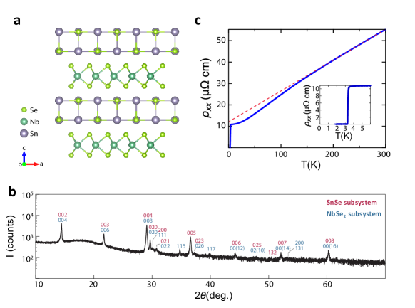
Here, we investigate the impact of dimensionality on the CDW in -NbSe2 by utilizing a misfit crystal of [SnSe]1.16NbSe2 [17]. This incommensurate structure consists of single-layer -NbSe2 separated by rock-salt spacers of SnSe (see Fig. 1a and Supplementary Information). We demonstrate that such superstructure enables us to effectively study the intrinsic properties of monolayer -NbSe2. To achieve this, we first identify the material’s superconducting critical temperature (T) through transport measurements and measure its low-energy band structure using angle-resolved photoemission spectroscopy (ARPES). Finally, we probe the emergence of the CDW by tracking its collective mode dynamics as a function of temperature via spontaneous Raman scattering. Our findings reveal that TCDW is considerably enhanced in comparison to bulk -NbSe2, indicating that reduced dimensionality has a significant impact on the CDW phase. These results, obtained in a protected monolayer within the misfit bulk crystal, offer a clean approach to studying the CDW in the monolayer limit while minimizing environmental effects.


We first evaluate the conduction properties and electronic structure of the misfit crystal to demonstrate its effective two-dimensional behavior. Figure 1c shows the material’s resistivity as a function of temperature (see Supplementary Information). We find that TC is 3.2 K, consistent with values reported in monolayer -NbSe2 systems [7, 3] and [SnSe]1.16NbSe2 [18].
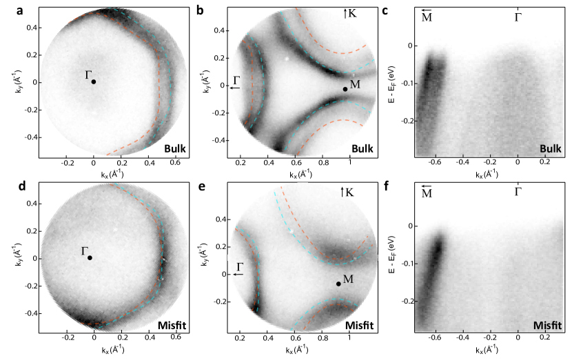
Next, we compare the electronic band structure of the misfit crystal with those expected for bulk and monolayer -NbSe2. To this end, we performed ARPES measurements of both [SnSe]1.16NbSe2 and bulk -NbSe2 under the same experimental conditions (see Supplementary Information). In Figs. 2a-c, we present the results for the bulk crystal, where we observe two hexagonal contours around the point and two warped triangular contours around the K point, all of which are associated with Nb 4d bands. Additionally, the signal at the zone center corresponds to Se 4pz derived ’pancake’ surface. These observations are consistent with previous measurements of bulk -NbSe2 [19, 20]. Examination of the measured band structure of the misfit crystal (Figure 2d-e) reveals three features that indicate behavior alike that of monolayer -NbSe2. Firstly, the misfit lacks a large inter-layer driven splitting of the contours around the point, which instead appears for the bulk. Secondly, we observe a circular inner contour around the point rather than the hexagonal one seen in the bulk. Thirdly, the spectral weight at the zone center is absent, which is consistent with the fact that the Se 4pz band does not cross the Fermi level in the monolayer limit. These observations are in excellent agreement with density functional theory calculations for a bulk and monolayer -NbSe2, which are superimposed on the experimental data in Fig. 2. In general, charge transfer from the rock-salt layer may dope the TMD layer, as previously demonstrated in other misfit compounds [21]. The comparison with the calculated Fermi surface indicates negligible charge transfer in our case, which is also consistent with previous studies [22, 23], making it a faithful representation of an isolated monolayer -NbSe2. It is worth noting that the energy resolution of our ARPES measurements (E 60 meV) did not allow us to detect CDW-induced changes in the band structure.
Both the measured conductivity and electronic band structure establish the presence of an effective monolayer -NbSe2 within the misfit bulk crystal. This allows us to probe the CDW in -NbSe2 at the monolayer limit while the monolayer resides within a bulk crystal environment.
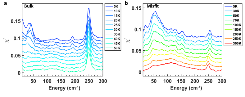
An electron-phonon-mediated CDW phase can be probed by monitoring its collective excitations – the amplitude and phase modes – typically via Raman or infrared spectroscopy, respectively. Here, we perform back to back Raman measurements of [SnSe]1.16NbSe2 and bulk -NbSe2 and observe the CDW amplitude mode in both crystals as a function of temperature (see experimental details in Supplementary Information). Figure 3 shows the temperature dependent Raman susceptibility in the bulk and misfit crystals, taken with crossed polarization configuration.

At room temperature, the Raman spectrum of the misfit crystal resembles the bulk Raman spectrum at TTCDW, with the appearance of the E2g phonon mode around 250 cm-1. Upon cooling below the bulk CDW transition temperature of 33.5 K, we observe the expected Raman response of bulk -NbSe2 [24, 25]: it develops a strong CDW amplitude mode centered around 40 cm-1, which softens in the temperature range of 30 K and 5 K, and an additional temperature dependent peak at 190 cm-1. On the other hand, the misfit crystal develops a strong new Raman mode centered around 50 cm-1 at a significantly higher temperature of about 250 K. Besides the modes that are associated with the -NbSe2 layer, we identify 3 phonon modes of SnSe [26] at 109 cm-1, 131 cm-1 and 153 cm-1.
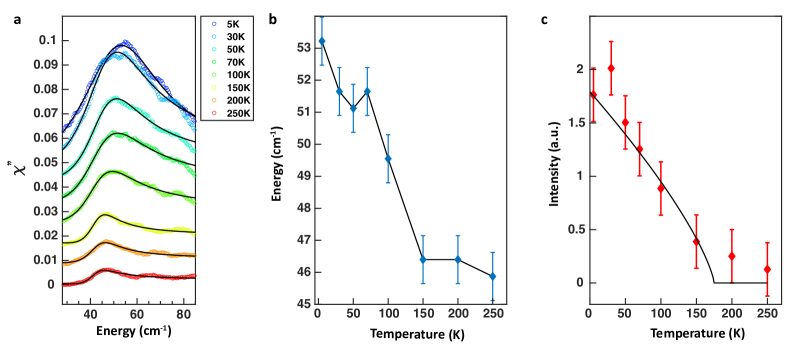
Figure 4a shows the temperature dependence of the amplitude mode after background subtraction. A fit of the mode (black lines in Figure 4a) shows a clear softening within the temperature range of 250 K and 5 K, where the temperature dependent central energy is presented in Figure 4b. Such softening indicates a shallower free energy potential surface for elevated temperatures, and identifies this peak with the amplitude mode of the CDW. In order to identify TCDW, we plot in Figure 4c the amplitude mode intensity as a function of temperature. We find good agreement with a mean field calculation (black line in Figure 4c, see Supplementary Information), which allows us to determine a transition temperature of about 175 K. An indirect indication for the enhanced CDW can be found by a closer examination of the resistivity measurements, manifested as a deviation from a linear response (represented by the red dashed line in Fig. 1c) starting at approximately 150 K. Such a kink is reminiscent, for example, of the transport signatures of the pseudogap in cuprates which as in the case of -NbSe2 becomes partially gaped below the transition temperature.
Indeed, as mentioned earlier, previous Raman measurements of exfoliated monolayer -NbSe2 showed a very similar temperature-dependent amplitude mode [7, 9], indicating a dramatic enhancement of the CDW phase. However, since the observed CDW enhancement in our experiments is based on a monolayer within a bulk crystal, we can safely rule out environmental factors that may induce such enhancement. This in turn leads us to determine that the origin of the enhancement is the reduced dimensionality of -NbSe2. Our finding resolves the main debate point between the contradicting reported results[8, 7, 12, 13] for the CDW properties at the monolayer limit.

The CDW phase forms once the system can find a lower energy ground state by mutual distortion of the charge distribution and the lattice [27]. This condition is realized when the electronic energy gain is greater than the lattice elastic energy loss. In the case of bulk -NbSe2, the inter-layer coupling contributes to the lattice elastic energy, meaning it makes it harder for the lattice to deform. In the monolayer limit, the inter-layer coupling does not play a role, which may increase the CDW stability [12]. Examination of the crystal structure of [SnSe]1.16NbSe2 [17] shows a significantly larger separation of single layers -NbSe2 compared to the van der Waals spacing of bulk -NbSe2 by a factor of 3. Such a large separation practically decouples the single layers, and therefore reduces the elastic energy cost of the CDW phase transition. As seen in previous studies [7, 9], this leads to a significant enhancement of the CDW in an exfoliated monolayer -NbSe2, whereas in the current study we show that the enhancement is a direct consequence of reduced dimensionality by probing the CDW at the monolayer limit within a protected misfit crystal.
Data availability
The data that support the plots within this paper and other finding of this study are available from the corresponding author upon reasonable request.
Acknowledgements
The authors thank Dongsung Choi for technical assistance during the ARPES measurements. D.A., E.B. and N.G. acknowledge support by the US Department of Energy, BES DMSE (data taking, analysis and manuscript writing) and Gordon and Betty Moore Foundation’s EPiQS Initiative grant GBMF9459 (instrumentation). D. A. acknowledges financial support by the Zuckerman STEM Leadership Program. P.W., A.D. and J.C. acknowledge support, in part, by the Gordon and Betty Moore Foundation EPiQS Initiative, Grant No. GBMF9070 to J.G.C (instrumentation development, DFT calculations), the US Department of Energy (DOE) Office of Science, Basic Energy Sciences, under award DE-SC0022028 (material development), and the Office of Naval Research (ONR) under award N00014-21-1-2591 (advanced characterization). P.O.W. acknowledges support from the STC Center for Integrated Quantum Materials (NSF grant DMR-1231319). J.L. and R.C. acknowledge support by the National Science Foundation under Grant No. 1751739.
Contributions
D.A. and E.B. performed the ARPES measurements; A.D. and P.W. synthesized the crystals and performed the transport measurements; J.L. performed the Raman measurements; S.F. performed the DFT calculations; D.A. analyzed the data and wrote the manuscript with contributions from all authors; R.C., J.C. and N.G. supervised the project.
Competing interests
The authors declare no competing interests.
Corresponding author
Nuh Gedik gedik@mit.edu
References
- Sajadi et al. [2018] E. Sajadi, T. Palomaki, Z. Fei, W. Zhao, P. Bement, C. Olsen, S. Luescher, X. Xu, J. A. Folk, and D. H. Cobden, Gate-induced superconductivity in a monolayer topological insulator, Science 362, 922 (2018).
- Yu et al. [2019] Y. Yu, L. Ma, P. Cai, R. Zhong, C. Ye, J. Shen, G. D. Gu, X. H. Chen, and Y. Zhang, High-temperature superconductivity in monolayer Bi2Sr2CaCu2O8+δ, Nature 575, 156 (2019).
- Xi et al. [2016a] X. Xi, Z. Wang, W. Zhao, J.-H. Park, K. T. Law, H. Berger, L. Forró, J. Shan, and K. F. Mak, Ising pairing in superconducting NbSe2 atomic layers, Nature Physics 12, 139 (2016a).
- Feng et al. [2018] J. Feng, D. Biswas, A. Rajan, M. D. Watson, F. Mazzola, O. J. Clark, K. Underwood, I. Markovic, M. McLaren, A. Hunter, et al., Electronic structure and enhanced charge-density wave order of monolayer VSe2, Nano letters 18, 4493 (2018).
- Sugawara et al. [2016] K. Sugawara, Y. Nakata, R. Shimizu, P. Han, T. Hitosugi, T. Sato, and T. Takahashi, Unconventional charge-density-wave transition in monolayer 1T-TiSe2, ACS nano 10, 1341 (2016).
- Lu et al. [2015] J. Lu, O. Zheliuk, I. Leermakers, N. F. Yuan, U. Zeitler, K. T. Law, and J. Ye, Evidence for two-dimensional ising superconductivity in gated mos2, Science 350, 1353 (2015).
- Xi et al. [2015] X. Xi, L. Zhao, Z. Wang, H. Berger, L. Forró, J. Shan, and K. F. Mak, Strongly enhanced charge-density-wave order in monolayer NbSe2, Nature nanotechnology 10, 765 (2015).
- Ugeda et al. [2016] M. M. Ugeda, A. J. Bradley, Y. Zhang, S. Onishi, Y. Chen, W. Ruan, C. Ojeda-Aristizabal, H. Ryu, M. T. Edmonds, H.-Z. Tsai, et al., Characterization of collective ground states in single-layer NbSe2, Nature Physics 12, 92 (2016).
- Lin et al. [2020] D. Lin, S. Li, J. Wen, H. Berger, L. Forró, H. Zhou, S. Jia, T. Taniguchi, K. Watanabe, X. Xi, et al., Patterns and driving forces of dimensionality-dependent charge density waves in 2h-type transition metal dichalcogenides, Nature communications 11, 1 (2020).
- Xie et al. [2021] X. Xie, D. Lin, L. Zhu, Q. Li, J. Zong, W. Chen, Q. Meng, Q. Tian, S.-C. Li, X. Xi, et al., Charge density wave and electron-phonon interaction in epitaxial monolayer NbSe2 films, Chinese Physics Letters 38, 107101 (2021).
- Xi et al. [2016b] X. Xi, H. Berger, L. Forró, J. Shan, and K. F. Mak, Gate tuning of electronic phase transitions in two-dimensional NbSe2, Physical review letters 117, 106801 (2016b).
- Lian et al. [2018] C.-S. Lian, C. Si, and W. Duan, Unveiling charge-density wave, superconductivity, and their competitive nature in two-dimensional NbSe2, Nano letters 18, 2924 (2018).
- Bianco et al. [2020] R. Bianco, L. Monacelli, M. Calandra, F. Mauri, and I. Errea, Weak dimensionality dependence and dominant role of ionic fluctuations in the charge-density-wave transition of NbSe2, Physical Review Letters 125, 106101 (2020).
- Calandra et al. [2009] M. Calandra, I. Mazin, and F. Mauri, Effect of dimensionality on the charge-density wave in few-layer 2H-NbSe2, Physical Review B 80, 241108 (2009).
- Lin et al. [2022] D. Lin, A. Ranjbar, X. Li, X. Huang, Y. Huang, H. Berger, L. Forró, K. Watanabe, T. Taniguchi, R. V. Belosludov, et al., Axial-bonding-driven dimensionality effect on the charge-density wave in NbSe2, Nano Letters 22, 9389 (2022).
- Chen et al. [2020] Y. Chen, L. Wu, H. Xu, C. Cong, S. Li, S. Feng, H. Zhang, C. Zou, J. Shang, S. A. Yang, et al., Visualizing the anomalous charge density wave states in graphene/nbse2 heterostructures, Advanced Materials 32, 2003746 (2020).
- Ng and McQueen [2022] N. Ng and T. M. McQueen, Misfit layered compounds: Unique, tunable heterostructured materials with untapped properties, APL Materials 10, 100901 (2022).
- Bai et al. [2018] H. Bai, X. Yang, Y. Liu, M. Zhang, M. Wang, Y. Li, J. Ma, Q. Tao, Y. Xie, G.-H. Cao, et al., Superconductivity in a misfit layered compound (SnSe)1.16(NbSe2), Journal of Physics: Condensed Matter 30, 355701 (2018).
- Inosov et al. [2008] D. Inosov, V. Zabolotnyy, D. Evtushinsky, A. Kordyuk, B. Büchner, R. Follath, H. Berger, and S. Borisenko, Fermi surface nesting in several transition metal dichalcogenides, New Journal of Physics 10, 125027 (2008).
- Rossnagel et al. [2001] K. Rossnagel, O. Seifarth, L. Kipp, M. Skibowski, D. Voß, P. Krüger, A. Mazur, and J. Pollmann, Fermi surface of 2H-NbSe2 and its implications on the charge-density-wave mechanism, Physical Review B 64, 235119 (2001).
- Leriche et al. [2021] R. T. Leriche, A. Palacio-Morales, M. Campetella, C. Tresca, S. Sasaki, C. Brun, F. Debontridder, P. David, I. Arfaoui, O. Šofranko, et al., Misfit layer compounds: A platform for heavily doped 2D transition metal dichalcogenides, Advanced Functional Materials 31, 2007706 (2021).
- Wiegers and Zhou [1991] G. Wiegers and W. Zhou, The misfit layer compound (snse) 1.16 nbse2, Materials research bulletin 26, 879 (1991).
- Wiegers [1995] G. Wiegers, Charge transfer between layers in misfit layer compounds, Journal of Alloys and Compounds 219, 152 (1995).
- Sooryakumar and Klein [1980] R. Sooryakumar and M. Klein, Raman scattering by superconducting-gap excitations and their coupling to charge-density waves, Physical Review Letters 45, 660 (1980).
- Méasson et al. [2014] M.-A. Méasson, Y. Gallais, M. Cazayous, B. Clair, P. Rodiere, L. Cario, and A. Sacuto, Amplitude higgs mode in the 2H-NbSe2 superconductor, Physical Review B 89, 060503 (2014).
- Pal et al. [2020] S. Pal, R. Arora, S. Roychowdhury, L. Harnagea, K. Saurabh, S. Shenoy, D. Muthu, K. Biswas, U. Waghmare, and A. Sood, Pressure-induced phase transitions in the topological crystalline insulator snte and its comparison with semiconducting snse: Raman and first-principles studies, Physical Review B 101, 155202 (2020).
- Grüner [1988] G. Grüner, The dynamics of charge-density waves, Reviews of modern physics 60, 1129 (1988).