Centimeter-scale nanomechanical resonators with low dissipation
Abstract
High-aspect-ratio mechanical resonators are pivotal in precision sensing, from macroscopic gravitational wave detectors to nanoscale acoustics. However, fabrication challenges and high computational costs have limited the length-to-thickness ratio of these devices, leaving a largely unexplored regime in nano-engineering. We present for the first time nanomechanical resonators that extend centimeters in length yet retain nanometer thickness. We explore this new design space using an optimization approach which judiciously employs fast millimeter-scale simulations to steer the more computationally intensive centimeter-scale design optimization. The synergy between nanofabrication, design optimization guided by machine learning, and precision engineering opens a solid-state approach to room temperature quality factors of 10 billion at kilohertz mechanical frequencies – comparable to extreme performance of leading cryogenic resonators and levitated nanospheres, even under significantly less stringent temperature and vacuum conditions.
Mechanical resonators are crucial in precision sensing, enabling gravitational-wave observations at the macroscale1, 2, probing weak forces in atomic force microscopy at the nanoscale3, 4 or playing a central role in recent quantum technologies5, 6, 7. Their performance largely hinges on having low mechanical dissipation, quantified by the mechanical quality factor (Q). The Q factor measures both radiated acoustic energy and infiltrating thermomechanical noise, with a high Q pivotal in preserving resonator coherence. This is crucial, particularly at room temperature, for observing quantum phenomena8, 9, advancing quantum technology10, and maximizing sensitivity for detecting changes in mass11, 12, 13, force14, 15, and displacement1. High Q is often achieved through “dissipation dilution”, a phenomenon originating from the synergistic effects of large tensile stress and high-aspect-ratio, observed both in macroscale2, 16 and applied to nanoscale resonators17, 18, 19.
At the macroscale, a notable example is the suspension resonator in gravitation wave detectors 20, 21, where kilogram mirrors are suspended by wires tens of centimeters long and a thickness on the order of micrometers (Fig. 1b). The high tensile stress is created by loading them with mirror masses, which induce stress in the wires due to gravity. The resulting high quality factor of the order of allows isolating the detector from thermomechanical noise, enabling it to reach its enhanced displacement sensitivity. The exceptional acoustic isolation of these resonators has enabled landmark demonstrations of quantum effects at an unprecedented kilogram scale 22 and the first observations of gravitational waves 23. Similar configurations at smaller scales are employed on table-top experiments to investigate the limits of quantum mechanics 24 and its interplay with gravity 25. To date, all centimeter-scale mechanical resonators have been limited to micron-scale thicknesses.
At the nanoscale, resonators up to millimeters long and nanometers thin are built on-chip, utilizing substrate support (Fig. 1a). High tensile stress, generated through a thermal mismatch between the resonator and the substrate, offers both lower mechanical dissipation and structural stability for long-distance suspended nanostructures. This necessitates careful material selection, with silicon nitride (Si3N4) emerging as the optimal choice at room temperature. Leveraging standard silicon technology compatibility, these nanomechanical resonators provide scalability31, and integration5 not found in their macroscale counterparts. Techniques like mode-shape engineering26, 32, 33, 27, 28 and phononic crystal (PnC) engineering29, 30 have further enhanced dissipation dilution, pushing quality factors above . This improved coherence of motion has propelled advances in quantum phenomena exploration at cryogenic temperatures 34, 35 and fostered a new sensor class development36, 37.
Nanomechanical resonators have been restricted to millimeter lengths (Fig. 1d), limiting their achievable quality factor and operational frequency. Advancing these resonators to centimeter lengths while maintaining nanoscale thickness could both amplify dissipation dilution at room temperature and access an uncharted regime for on-chip nanomechanics, characterized by high quality factors, significant mass, and low resonance frequencies. This transition would catalyze a myriad of applications from ultralight dark matter detection 38 to quantum effects observation at room temperature 10. Yet, pursuing such extreme-aspect-ratios faces considerable computational and fabrication barriers, including the need for a high fabrication yield to offset the limited number of devices per chip and the profound cost implications. This challenge of cost-effective high-yield fabrication for centimeter-scale nanostructures introduces a unique dynamic between economics and design distinct from traditional high-volume nanotechnology.
We propose a novel approach that merges ultra-delicate fabrication techniques and multi-fidelity Bayesian optimization, enabling the creation of mechanical resonators with extraordinarily high-aspect-ratios exceeding ; equivalent to reliably producing ceramic structures with a thickness of 1 millimeter, suspended over nearly half a kilometer. This represents a type of geometry far from anything we observe at macroscopic scales. Our design strategy dramatically curtails optimization time while successfully circumventing common fabrication issues such as stiction, collapse and fracture. Applying our strategy to a long silicon nitride string, we achieved a quality factor exceeding at room temperature – the highest ever recorded for a mechanically clamped resonator. This solid-state platform performs on par with phenomenal counterparts such as optically levitated nanospheres which are completely isolated by extreme vacuum conditions as low as mbar39. In contrast, our clamped centimeter-scale resonators, can approach comparable dissipation levels at pressures nearly two orders of magnitude higher, removing the need for extreme-high-vacuum to achieve a quality factor approaching 10 billion. Notably, our room temperature resonators can also work at quality factors only observed in cryogenic counterparts 40, 41. This enhanced capability to operate at higher temperatures and pressures unveils the exceptional potentials in centimeter-scale nanotechnology, expanding the boundaries of what is achievable with on-chip, room temperature resonators.
High-aspect-ratio advantage and multi-fidelity design
The quality factor of strained thin one-dimensional mechanical resonators is given by 19
| (1) |
where is the intrinsic quality factor (surface loss), is the mode order, is the Young’s modulus, is the initial stress, and are the resonator’s length and thickness in the direction of motion, respectively. The second term in the denominator of Equation 1 originates from the sharp curvature at the clamps 18 where the resonator is anchored to the supporting substrate, whereas the first term accounts for the curvature along the remainder of the resonator, both depending on the aspect-ratio (Fig. 1c).
In the high-aspect-ratio limit, clamping loss is orders of magnitude larger, dominating the loss contribution. To this end, techniques known as soft clamping can be employed to reduce the sharp curvature at this region and improve the Q factor so that the Q factor scales quadratically with the aspect-ratio of the resonator. It is important to notice that a high aspect ratio is beneficial even if the Q factor is limited by the curvature at the clamping points (Equation 1). Hence, state-of-the-art high Q factor nanoresonators have advanced towards devices with increasing aspect-ratios, pushing the total length from micrometers 42, 26 to millimeters 28, 29, 30, 27 (Fig. 1c) alongside a thickness reduction below .
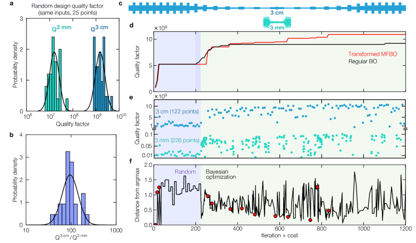
Centimeter-long resonators maintaining a thickness within tens of nanometers can significantly raise the achievable quality factor. However, these extreme-aspect-ratios and intricate cross-section variations necessitate high-fidelity computer simulations, rather than analytical models. Unfortunately, this approach imposes stringent discretization requirements due to the resonator’s oscillatory modes and extensive computation times. One optimization process took about 16 CPU-days for 150 iterations, which created a bottleneck in the design process. Here, multi-fidelity Bayesian optimization (MFBO) 43, 44, alternates between employing both a quick, low-fidelity model for resonators and a slower, high-fidelity model for ones. The high-fidelity predictions were eight times slower on average. The geometry of both resonators30 is parameterized (Supplementary Information Sec. I) to allow the presence of a PnC with a defect embedded in the center and chosen to practically allow the most number of on-chip resonators. The method then quickly explores the design space by fast evaluations of the smaller structures at higher frequencies (MHz), while establishing a correlation with the large devices at lower frequencies. This enables it to probe (slow) solutions for the high-aspect-ratio structures only on rare occasions when it expects the design to achieve a large quality factor.
The effectiveness of MFBO relies on the correlation between low and high-fidelity models and their respective evaluation times. If the low-fidelity model lacks correlation with the high-fidelity model, or if its evaluation time is comparable, the method loses effectiveness. By parameterizing the design space independently from resonator length (see Methods), we observed a reasonable correlation between the (low-fidelity) and the (high-fidelity) resonator designs (Fig. 2a). The Q factor of the design was a hundred times larger on average, but the optimal designs for both scales differed (Fig. 2b). Consequently, we applied MFBO to the log-normal Q factor, letting the algorithm selectively probe the design space via whichever fidelity it chooses. In essence, MFBO uses millimeter-scale simulations to guide centimeter-scale optimization.
Our method’s significant advantage is shown in Fig. 2d, as it finds designs with Q exceeding 10 billion – a first-of-its-kind result. We used multi-fidelity Bayesian optimization (transformed MFBO) to maximize the quality factor, outperforming single-fidelity Bayesian optimization (regular BO) by approximately 20%. Figure 2c depicts the optimized geometry. After determining the optimal design, we focused on fabricating this high-aspect-ratio device. The optimized geometry follows a similar result suggested by Ghadimi et al. 30 with a tapered shape maximizing the width around the clamping region, but the central defect in the PnC was not the region with the highest stress level as in previous designs. Designs having stress concentration around the clamping region 45 were also considered during the optimization to have high-quality factors, which can be found in the Supplementary Video, but they exhibited worse performance. Once the best design was found, we focused on addressing the challenges of fabricating a device with such an extreme-aspect-ratio.
Centimeter scale nanofabrication
Manufacturing centimeter-scale nano-components relies on fabrication intuition that shift from conventional nanotechnologies, requiring a shift in design principles, fabrication methods, and cost considerations. In accordance with Moore’s Law, conventional nanotechnology has focused on miniaturization across all three dimensions (x, y, z). However, centimeter-scale nanotechnology marks a significant transition that requires components expanding out to macroscopic lengths in x and/or y while retaining their nanoscale thickness. These nanostructures not only have extreme-aspect-ratios at the macro-scale, but they are also intricately nanopatterned at the micro-scale, imbuing them with enhanced functionalities (mechanical, optical, etc.) that transcend conventional nanotechnology. In particular, our nanostrings are not just elongated and thin; they also incorporate precisely patterned phononic bandgaps, enabling novel acoustic capabilities that surpass those achievable at smaller scales.
In contrast to conventional miniaturization, the size constraints of centimeter-scale nanostructures permit far fewer devices per wafer, requiring excellent fabrication yields due to the significantly higher costs per device. Given their long geometries, any fracture of a centimeter-scale nanostructure not only results in fewer successful devices but these broken devices can also collapse over several neighboring structures, significantly escalating the cost implications of fabrication errors and low yield. Moreover, the fabrication of these high-aspect-ratio structures requires them to be released with delicate nanofabrication techniques that do not exert any destructive forces during and after suspension. These processes must ensure that the high-aspect-ratio structures remain unfractured and undistorted, and are positioned safely away from nearby surfaces to prevent potential issues such as stiction due to attractive surface forces.
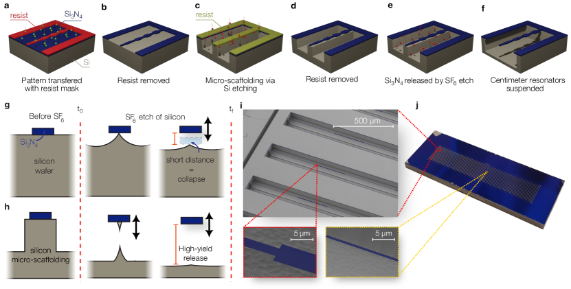
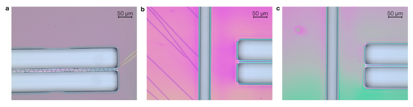
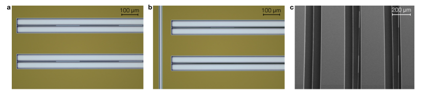
The schematic of the fabrication procedure is shown in Fig. 3a-f (see Methods). First, high-stress (1.07GPa) Si3N4 is deposited on a silicon wafer. A resist layer is spun on and lithographically patterned with an array of the long optimized PnC resonators. This patterned resist is used as a mask to transfer the design into the Si3N4 film via directional plasma etch (Fig. 3a). Typically the most crucial step is the careful release of these fragile structures by removing the silicon beneath the Si3N4 resonator; with centimeter-scale nanostructures the requirements for successful suspension become much more stringent.
A critical aspect to realizing these nanostructures is the high stress within Si3N4 which not only contributes to achieving a high Q factor but also provides the required structural support and stability, allowing these taut strings to remain free-standing over remarkable distances without collapsing or sagging. In particular, we use dry SF6 plasma etch to remove the silicon under the Si3N4 resonator (Fig. 3c-f) since it avoids the conventional stiction and collapse from surface tension present in liquid etchants46. Once released, these -long, -thick structures can displace tens of microns due to handling and static charge build up. In combination with the SF6 plasma dry release, we first engineer a micro-scaffolding30 (Fig. 3g,h) into the silicon underneath our Si3N4 that allows the free-standing structures to be suspended quickly, delicately, and far away from the substrate below; significantly increasing the yield and viability of this new type of nanotechnology (Supplementary Information Sec. E).
Our choice to focus on 1D PnC nanostrings comes from a practical standpoint, which allows for packing numerous devices per chip (Fig 3i,j). By carefully engineering the ultra-delicate release of these structures, we achieved a fabrication yield as high as 93% on our best chip and 75% over all chips processed. While we only study 1D structures, the methodologies we developed are versatile and can be readily applied to more complex structures such as 2D phononic shields 29.
Low dissipation at room temperature
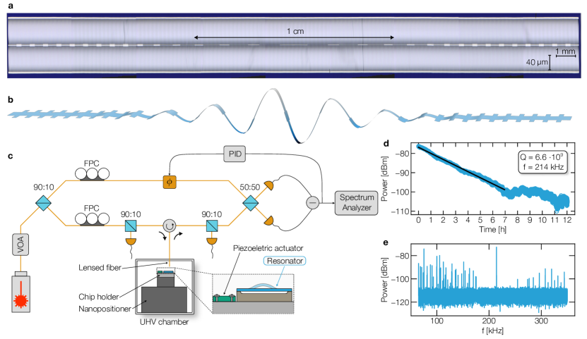
To assess the mechanical properties of the fabricated nanoresonators (Fig. 4a), we characterized the strings’ out-of-plane displacements by a balanced homodyne optical interferometer (Fig. 4c) built to experimentally measure the nanoresonators. The nanoresonator is placed inside an ultra-high vacuum (UHV) chamber at P mbar to avoid gas damping, increasingly dominant for high-aspect-ratio structures (see Supplementary Information Sec. A), and mechanically excited by a piezoelectric actuator. The resonator’s motion is detected by an infrared laser via a lensed fiber. Figure 4e shows the displacement spectrum obtained from a location near the center of the string, under thermal excitation. The spectrum shows a clear bandgap in frequency between and with one localized mode inside. The latter is observed at , in good agreement with simulation prediction. Figure 4b shows the predicted mode shapes obtained by finite element analysis for the eigenmode in the center of the bandgap. On the contrary, outside the - range, a plethora of modes are detected, whose displacement is distributed over the entire string length.
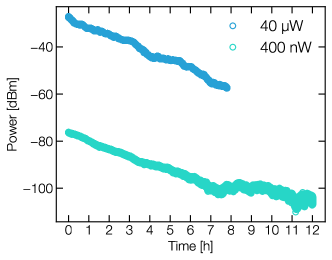
We experimentally evaluate the quality factor of the nanoresonators by applying a sinusoidal function to the piezoelectric actuator at a frequency near the eigenfrequency of the localized mode. Once the displacement at resonance reaches a plateau, the excitation is abruptly turned off to measure the ringdown of the mechanical mode. Figure 4d shows the envelope of the obtained signal where the measured decay rate is proportional to the nanoresonator energy dissipation and thus its quality factor. As Fig. 4d shows, the localized mode at decays for over 7 hours. This corresponds to a Q factor of 6.6 billion at room temperature, to the best of our knowledge the highest value yet measured for a solid-state resonator.
While our simulations expect Qs of 10 billion, the fabricated centimeter scale nanomechanical structures have high-aspect-ratios that make it difficult to dissipate heat during the (exothermic) undercut process (Fig 3e), resulting in different Si3N4 etch rates. This gives the nanostructures slightly different thickness and dimension from edge to center along the beam, thus reducing the fidelity between design and experiment (Supplementary Information Sec. B).
Conclusion
We demonstrated centimetre-scale nanomechanical resonators with aspect-ratio above . Our approach combines two features. First, using MFBO we are able to reduce the simulation cost while maintaining the required accuracy to precisely capture the resonator’s behaviour. The resulting data-driven design process allows to optimize PnC strings obtaining soft-clamped modes which eliminate clamping losses and radiation to the substrate. Second, a dry etching technique that overcomes limitations such as stiction and collapse enables to reliably realize the optimized designs on-chip. The fabricated PnC strings extend for in length maintaining nanometers thickness and a minimum width of . With a Q of 6.6 billion at a frequency of , we experimentally achieve the lowest dissipation ever observed for a solid-state resonator at room temperature.
The obtained aspect-ratio enables not only to achieve unprecedented quality factors for on-chip resonators in room temperature environments, but it also leads to low resonance frequencies and large spacing between nearby mechanical modes. Those features translate into many-fold advantages as coherence time approaching 1 ms, thermomechanical-limited force sensitivity of \unitaN/Hz and thermomechanical limited Allan deviation47 reaching .
A natural quantum application is ground state cooling in a room-temperature environment. The high coherence time enables these resonators to undergo more than 200 coherent oscillations in the ground state before a thermal phonon enters the system 48. The small thermal decoherence rate of a few Hz allows to resolve the zero point fluctuations with a displacement imprecision below , on pair with the imprecision limit due to shot noise achievable in conventional interferometer setup. This makes centimeter-scale nanoresonators particularly promising for the cavity-free cooling scheme49. The developed resonators are also ideal candidates for creating high-precision sensors, specifically force detectors 15, and hold promise for obtaining frequency stability on pair with state-of-the-art clocks 50, 47, 51.
Remarkably, the degree of acoustic isolation (quantified by the quality factor) we can achieve on a solid-state microchip is similar to extraordinary values recently demonstrated for optically levitated nanoparticles operating at vacuum pressure levels more than two orders of magnitude lower than our resonators 39, 52. This is particularly striking if one considers that levitated particles do not have any physical connection with the environment except for the small coupling to any gas molecules still present at extremely high vacuums of mbar. On the contrary, our solid-state resonators are physically clamped to a room temperature chip, surrounded by 100 times higher gas pressures and exhibit comparable acoustic dissipation.
The ability to combine macromechanics with nanomechanics offers unique possibilities to integrate the versatility of on-chip technology with the detection sensitivity of macroscale resonators. Notably, the only foreseeable limitation to producing even longer, higher-Q devices is that larger undercuts distance must be engineered, and practically going to longer, lower-frequency devices would require increasingly higher vacuum levels; this makes centimeter-scale nanotechnology particularly interesting for next-generation space applications53, 54 which inherently operate at pressures below mbar. Pushing the boundaries of fabrication capabilities with higher selectivity materials55, 40, 56 would extend our current approach to more extreme-aspect-ratios and investigate new physics. These include the exploration of weak forces such as ultralight dark matter 38 and the investigation of gravitational effects at the nanoscale 57, 58. By blurring the line between macroscopic and nanoscale objects, these centimeter-scale nanomechanical systems challenge our conventional intuitions about fabrication, costs, and computer design and promise to give us novel capabilities which have not been available at smaller scales.
References
- Abramovici et al. 1992 A. Abramovici, W. E. Althouse, R. W. P. Drever, Y. Gürsel, S. Kawamura, F. J. Raab, D. Shoemaker, L. Sievers, R. E. Spero, K. S. Thorne, R. E. Vogt, R. Weiss, S. E. Whitcomb, and M. E. Zucker, Science 256, 325 (1992).
- González and Saulson 1994 G. I. González and P. R. Saulson, The Journal of the Acoustical Society of America 96, 207 (1994).
- Harris et al. 2015 J. Harris, P. Rabl, and A. Schliesser, Annalen der Physik 527, A13 (2015).
- Zhang et al. 2022 S.-D. Zhang, J. Wang, Y.-F. Jiao, H. Zhang, Y. Li, Y.-L. Zuo, Ş. K. Özdemir, C.-W. Qiu, F. Nori, and H. Jing, arXiv:2202.08690 [quant-ph] (2022), arxiv:2202.08690 [quant-ph] .
- Guo et al. 2019 J. Guo, R. Norte, and S. Gröblacher, Physical Review Letters 123, 223602 (2019).
- Mason et al. 2019 D. Mason, J. Chen, M. Rossi, Y. Tsaturyan, and A. Schliesser, Nature Physics 15, 745 (2019).
- Saarinen et al. 2023 S. A. Saarinen, N. Kralj, E. C. Langman, Y. Tsaturyan, and A. Schliesser, Optica 10, 364 (2023).
- Seis et al. 2022 Y. Seis, T. Capelle, E. Langman, S. Saarinen, E. Planz, and A. Schliesser, Nature Communications 13, 1507 (2022).
- Midolo et al. 2018 L. Midolo, A. Schliesser, and A. Fiore, Nature Nanotechnology 13, 11 (2018).
- Magrini et al. 2021a L. Magrini, P. Rosenzweig, C. Bach, A. Deutschmann-Olek, S. G. Hofer, S. Hong, N. Kiesel, A. Kugi, and M. Aspelmeyer, Nature 595, 373 (2021a).
- Manzaneque et al. 2020 T. Manzaneque, P. G. Steeneken, F. Alijani, and M. K. Ghatkesar, IEEE Sensors Journal , 1 (2020).
- Chen et al. 2021 X. Chen, N. Kothari, A. Keşkekler, P. G. Steeneken, and F. Alijani, Sensors and Actuators A: Physical 330, 112842 (2021).
- Hanay et al. 2015 M. S. Hanay, S. I. Kelber, C. D. O’Connell, P. Mulvaney, J. E. Sader, and M. L. Roukes, Nature Nanotechnology 10, 339 (2015).
- Reinhardt et al. 2016 C. Reinhardt, T. Müller, A. Bourassa, and J. C. Sankey, Physical Review X 6, 021001 (2016).
- Eichler 2022 A. Eichler, Materials for Quantum Technology 2, 043001 (2022).
- Cagnoli et al. 2000 G. Cagnoli, J. Hough, D. DeBra, M. Fejer, E. Gustafson, S. Rowan, and V. Mitrofanov, Physics Letters A 272, 39 (2000).
- Unterreithmeier et al. 2010 Q. P. Unterreithmeier, T. Faust, and J. P. Kotthaus, Physical Review Letters 105, 027205 (2010).
- Schmid et al. 2011 S. Schmid, K. Jensen, KH. K Nielsen, and A. Boisen, Physical Review B 84, 1 (2011).
- Yu et al. 2012 P.-L. Yu, T. P. Purdy, and C. A. Regal, Physical Review Letters 108, 083603 (2012).
- Cumming et al. 2012 A. V. Cumming, A. S. Bell, L. Barsotti, M. A. Barton, G. Cagnoli, D. Cook, L. Cunningham, M. Evans, G. D. Hammond, G. M. Harry, A. Heptonstall, J. Hough, R. Jones, R. Kumar, R. Mittleman, N. A. Robertson, S. Rowan, B. Shapiro, K. A. Strain, K. Tokmakov, C. Torrie, and A. A. van Veggel, Classical and Quantum Gravity 29, 035003 (2012).
- Dawid and Kawamura 1997 D. J. Dawid and S. Kawamura, Review of Scientific Instruments 68, 4600 (1997).
- Whittle et al. 2021 C. Whittle, E. D. Hall, S. Dwyer, N. Mavalvala, V. Sudhir, R. Abbott, A. Ananyeva, C. Austin, L. Barsotti, J. Betzwieser, C. D. Blair, A. F. Brooks, D. D. Brown, A. Buikema, C. Cahillane, J. C. Driggers, A. Effler, A. Fernandez-Galiana, P. Fritschel, V. V. Frolov, T. Hardwick, M. Kasprzack, K. Kawabe, N. Kijbunchoo, J. S. Kissel, G. L. Mansell, F. Matichard, L. McCuller, T. McRae, A. Mullavey, A. Pele, R. M. S. Schofield, D. Sigg, M. Tse, G. Vajente, D. C. Vander-Hyde, H. Yu, H. Yu, C. Adams, R. X. Adhikari, S. Appert, K. Arai, J. S. Areeda, Y. Asali, S. M. Aston, A. M. Baer, M. Ball, S. W. Ballmer, S. Banagiri, D. Barker, J. Bartlett, B. K. Berger, D. Bhattacharjee, G. Billingsley, S. Biscans, R. M. Blair, N. Bode, P. Booker, R. Bork, A. Bramley, K. C. Cannon, X. Chen, A. A. Ciobanu, F. Clara, C. M. Compton, S. J. Cooper, K. R. Corley, S. T. Countryman, P. B. Covas, D. C. Coyne, L. E. H. Datrier, D. Davis, C. Di Fronzo, K. L. Dooley, P. Dupej, T. Etzel, M. Evans, T. M. Evans, J. Feicht, P. Fulda, M. Fyffe, J. A. Giaime, K. D. Giardina, P. Godwin, E. Goetz, S. Gras, C. Gray, R. Gray, A. C. Green, E. K. Gustafson, R. Gustafson, J. Hanks, J. Hanson, R. K. Hasskew, M. C. Heintze, A. F. Helmling-Cornell, N. A. Holland, J. D. Jones, S. Kandhasamy, S. Karki, P. J. King, R. Kumar, M. Landry, B. B. Lane, B. Lantz, M. Laxen, Y. K. Lecoeuche, J. Leviton, J. Liu, M. Lormand, A. P. Lundgren, R. Macas, M. MacInnis, D. M. Macleod, S. Márka, Z. Márka, D. V. Martynov, K. Mason, T. J. Massinger, R. McCarthy, D. E. McClelland, S. McCormick, J. McIver, G. Mendell, K. Merfeld, E. L. Merilh, F. Meylahn, T. Mistry, R. Mittleman, G. Moreno, C. M. Mow-Lowry, S. Mozzon, T. J. N. Nelson, P. Nguyen, L. K. Nuttall, J. Oberling, R. J. Oram, C. Osthelder, D. J. Ottaway, H. Overmier, J. R. Palamos, W. Parker, E. Payne, R. Penhorwood, C. J. Perez, M. Pirello, H. Radkins, K. E. Ramirez, J. W. Richardson, K. Riles, N. A. Robertson, J. G. Rollins, C. L. Romel, J. H. Romie, M. P. Ross, K. Ryan, T. Sadecki, E. J. Sanchez, L. E. Sanchez, T. R. Saravanan, R. L. Savage, D. Schaetz, R. Schnabel, E. Schwartz, D. Sellers, T. Shaffer, B. J. J. Slagmolen, J. R. Smith, S. Soni, B. Sorazu, A. P. Spencer, K. A. Strain, L. Sun, M. J. Szczepańczyk, M. Thomas, P. Thomas, K. A. Thorne, K. Toland, C. I. Torrie, G. Traylor, A. L. Urban, G. Valdes, P. J. Veitch, K. Venkateswara, G. Venugopalan, A. D. Viets, T. Vo, C. Vorvick, M. Wade, R. L. Ward, J. Warner, B. Weaver, R. Weiss, B. Willke, C. C. Wipf, L. Xiao, H. Yamamoto, L. Zhang, M. E. Zucker, and J. Zweizig, Science 372, 1333 (2021).
- Abbott et al. 2016 B. P. Abbott, R. Abbott, T. Abbott, M. Abernathy, F. Acernese, K. Ackley, C. Adams, T. Adams, P. Addesso, R. Adhikari, et al., Physical review letters 116, 061102 (2016).
- Corbitt et al. 2007 T. Corbitt, C. Wipf, T. Bodiya, D. Ottaway, D. Sigg, N. Smith, S. Whitcomb, and N. Mavalvala, Physical Review Letters 99, 160801 (2007).
- Matsumoto et al. 2019a N. Matsumoto, S. B. Cataño-Lopez, M. Sugawara, S. Suzuki, N. Abe, K. Komori, Y. Michimura, Y. Aso, and K. Edamatsu, Physical Review Letters 122, 071101 (2019a).
- Norte et al. 2016 R. A. Norte, J. P. Moura, and S. Gröblacher, Physical Review Letters 116, 10.1103/PhysRevLett.116.147202 (2016).
- Bereyhi et al. 2022a M. J. Bereyhi, A. Arabmoheghi, A. Beccari, S. A. Fedorov, G. Huang, T. J. Kippenberg, and N. J. Engelsen, Physical Review X 12, 021036 (2022a).
- Shin et al. 2022 D. Shin, A. Cupertino, M. H. J. de Jong, P. G. Steeneken, M. A. Bessa, and R. A. Norte, Advanced Materials 34, 2106248 (2022).
- Tsaturyan et al. 2017 Y. Tsaturyan, A. Barg, E. S. Polzik, and A. Schliesser, Nature Nanotechnology 12, 776 (2017).
- Ghadimi et al. 2018 A. H. Ghadimi, S. A. Fedorov, N. J. Engelsen, M. J. Bereyhi, R. Schilling, D. J. Wilson, and T. J. Kippenberg, Science 360, 764 (2018).
- Westerveld et al. 2021 W. J. Westerveld, M. Mahmud-Ul-Hasan, R. Shnaiderman, V. Ntziachristos, X. Rottenberg, S. Severi, and V. Rochus, Nature Photonics 15, 341 (2021).
- Bereyhi et al. 2022b M. J. Bereyhi, A. Beccari, R. Groth, S. A. Fedorov, A. Arabmoheghi, T. J. Kippenberg, and N. J. Engelsen, Nature Communications 13, 3097 (2022b).
- Pratt et al. 2023a J. R. Pratt, A. R. Agrawal, C. A. Condos, C. M. Pluchar, S. Schlamminger, and D. J. Wilson, Physical Review X 13, 011018 (2023a).
- Rossi et al. 2018 M. Rossi, D. Mason, J. Chen, Y. Tsaturyan, and A. Schliesser, Nature 563, 53 (2018).
- Purdy et al. 2013 T. P. Purdy, R. W. Peterson, and C. A. Regal, Science 339, 801 (2013).
- Hälg et al. 2021 D. Hälg, T. Gisler, Y. Tsaturyan, L. Catalini, U. Grob, M.-D. Krass, M. Héritier, H. Mattiat, A.-K. Thamm, R. Schirhagl, E. C. Langman, A. Schliesser, C. L. Degen, and A. Eichler, Physical Review Applied 15, L021001 (2021).
- Chaste et al. 2012 J. Chaste, A. Eichler, J. Moser, G. Ceballos, R. Rurali, and A. Bachtold, Nature Nanotechnology 7, 301 (2012).
- Manley et al. 2021 J. Manley, M. D. Chowdhury, D. Grin, S. Singh, and D. J. Wilson, Physical Review Letters 126, 061301 (2021).
- Dania et al. 2023 L. Dania, D. S. Bykov, F. Goschin, M. Teller, and T. E. Northup, Ultra-high quality factor of a levitated nanomechanical oscillator (2023), arxiv:2304.02408 [quant-ph] .
- Beccari 2022 A. Beccari, Nature Physics , 13 (2022).
- Ren et al. 2020 H. Ren, M. H. Matheny, G. S. MacCabe, J. Luo, H. Pfeifer, M. Mirhosseini, and O. Painter, Nature Communications 11, 3373 (2020).
- Thompson et al. 2008 J. Thompson, B. Zwickl, A. Jayich, F. Marquardt, S. Girvin, and J. Harris, Nature 452, 72 (2008).
- Poloczek et al. 2017 M. Poloczek, J. Wang, and P. I. Frazier, in Proceedings of the 31st International Conference on Neural Information Processing Systems (2017) pp. 4291–4301.
- Wu et al. 2020 J. Wu, S. Toscano-Palmerin, P. I. Frazier, and A. G. Wilson, in Uncertainty in Artificial Intelligence (PMLR, 2020) pp. 788–798.
- Bereyhi et al. 2019 M. J. Bereyhi, A. Beccari, S. A. Fedorov, A. H. Ghadimi, R. Schilling, D. J. Wilson, N. J. Engelsen, and T. J. Kippenberg, Nano letters 19, 2329 (2019).
- Norte 2015 R. A. Norte, Nanofabrication for On-Chip Optical Levitation, Atom-Trapping, and Superconducting Quantum Circuits, Ph.D. thesis, California Institute of Technology (2015).
- Manzaneque et al. 2023 T. Manzaneque, M. K. Ghatkesar, F. Alijani, M. Xu, R. A. Norte, and P. G. Steeneken, Physical Review Applied 19, 054074 (2023).
- Aspelmeyer et al. 2014 M. Aspelmeyer, T. J. Kippenberg, and F. Marquardt, Reviews of Modern Physics 86, 1391 (2014).
- Pluchar et al. 2020 C. M. Pluchar, A. R. Agrawal, E. Schenk, D. J. Wilson, and D. J. Wilson, Applied Optics 59, G107 (2020).
- Sadeghi et al. 2020 P. Sadeghi, A. Demir, L. G. Villanueva, H. Kähler, and S. Schmid, Physical Review B 102, 214106 (2020).
- Lewis 1991 L. Lewis, Proceedings of the IEEE 79, 927 (1991).
- Magrini et al. 2021b L. Magrini, P. Rosenzweig, C. Bach, A. Deutschmann-Olek, S. G. Hofer, S. Hong, N. Kiesel, A. Kugi, and M. Aspelmeyer, Nature 595, 373 (2021b).
- El-Sheimy and Youssef 2020 N. El-Sheimy and A. Youssef, Satellite Navigation 1, 1 (2020).
- Amaro-Seoane et al. 2012 P. Amaro-Seoane, S. Aoudia, S. Babak, P. Binetruy, E. Berti, A. Bohe, C. Caprini, M. Colpi, N. J. Cornish, K. Danzmann, et al., Classical and Quantum Gravity 29, 124016 (2012).
- Xu et al. 2023 M. Xu, D. Shin, P. M. Sberna, R. van der Kolk, A. Cupertino, M. A. Bessa, and R. A. Norte, arXiv preprint arXiv:2307.01271 (2023).
- Manjeshwar et al. 2023 S. K. Manjeshwar, A. Ciers, F. Hellman, J. Blasing, A. Strittmatter, and W. Wieczorek, Nano Letters (2023).
- Pratt et al. 2023b J. Pratt, A. Agrawal, C. Condos, C. Pluchar, S. Schlamminger, and D. Wilson, Physical Review X 13, 011018 (2023b), publisher: American Physical Society.
- Matsumoto et al. 2019b N. Matsumoto, M. Sugawara, S. Suzuki, N. Abe, K. Komori, Y. Michimura, Y. Aso, S. B. Cataño-Lopez, and K. Edamatsu, Physical Review Letters 122, 071101 (2019b), arxiv:1809.05081 .
- Inc. 2018 C. Inc., Comsol (2018).
- Fedorov et al. 2019 S. A. Fedorov, N. J. Engelsen, A. H. Ghadimi, M. J. Bereyhi, R. Schilling, D. J. Wilson, and T. J. Kippenberg, Physical Review B 99, 054107 (2019).
- Balandat et al. 2020 M. Balandat, B. Karrer, D. Jiang, S. Daulton, B. Letham, A. G. Wilson, and E. Bakshy, Advances in neural information processing systems 33, 21524 (2020).
- Dougherty et al. 2001 D. J. Dougherty, R. E. Muller, P. D. Maker, and S. Forouhar, Journal of Lightwave Technology 19, 1527 (2001).
- Moura et al. 2018 J. P. Moura, R. A. Norte, J. Guo, C. Schäfermeier, and S. Gröblacher, Optics Express 26, 1895 (2018).
- Norte et al. 2018 R. A. Norte, M. Forsch, A. Wallucks, I. Marinkovic, and S. Gröblacher, Physical Review Letters 121, 030405 (2018), arxiv:1806.10151 .
- Maduro et al. 2021 L. Maduro, C. de Boer, M. Zuiddam, E. Memisevic, and S. Conesa-Boj, Physica E: Low-dimensional Systems and Nanostructures 134, 114903 (2021).
- Sainiemi and Franssila 2007 L. Sainiemi and S. Franssila, Journal of Vacuum Science & Technology B: Microelectronics and Nanometer Structures Processing, Measurement, and Phenomena 25, 801 (2007).
- Schmid et al. 2023 S. Schmid, L. G. Villanueva, and M. L. Roukes, Fundamentals of Nanomechanical Resonators (Springer International Publishing, Cham, 2023).
- Verbridge et al. 2008 S. S. Verbridge, R. Ilic, H. G. Craighead, and J. M. Parpia, Applied Physics Letters 93, 013101 (2008).
- Henry et al. 2009 M. D. Henry, C. Welch, and A. Scherer, Journal of Vacuum Science & Technology A 27, 1211 (2009).
- Jones et al. 1998 D. R. Jones, M. Schonlau, and W. J. Welch, Journal of Global optimization 13, 455 (1998).
- Frazier 2018 P. I. Frazier, arXiv preprint arXiv:1807.02811 (2018).
- Snoek et al. 2012 J. Snoek, H. Larochelle, and R. P. Adams, in Advances in Neural Information Processing Systems 25, edited by F. Pereira, C. J. C. Burges, L. Bottou, and K. Q. Weinberger (Curran Associates, Inc., 2012) pp. 2951–2959.
- Shahriari et al. 2015 B. Shahriari, K. Swersky, Z. Wang, R. P. Adams, and N. De Freitas, Proceedings of the IEEE 104, 148 (2015).
- Kennedy and O’Hagan 2000 M. C. Kennedy and A. O’Hagan, Biometrika 87, 1 (2000).
- Han and Görtz 2012 Z.-H. Han and S. Görtz, AIAA journal 50, 1885 (2012).
- Le Gratiet and Garnier 2014 L. Le Gratiet and J. Garnier, International Journal for Uncertainty Quantification 4 (2014).
- Williams et al. 2007 C. Williams, E. V. Bonilla, and K. M. Chai, Advances in neural information processing systems , 153 (2007).
- Liu et al. 2018 H. Liu, J. Cai, and Y.-S. Ong, Knowledge-Based Systems 144, 102 (2018).
- Forrester et al. 2007 A. I. Forrester, A. Sóbester, and A. J. Keane, Proceedings of the royal society a: mathematical, physical and engineering sciences 463, 3251 (2007).
- Huang et al. 2006 D. Huang, T. T. Allen, W. I. Notz, and R. A. Miller, Structural and Multidisciplinary Optimization 32, 369 (2006).
- Jiang et al. 2019 P. Jiang, J. Cheng, Q. Zhou, L. Shu, and J. Hu, AIAA Journal 57, 5416 (2019).
Methods
Computational experiments and design. The design approach for high-aspect-ratio resonators was based on numerical analysis with COMSOL 59. The quality factor was maximized via multi-fidelity Bayesian optimization without recurring to the analytical solution derived for beam-like Phononic Crystals (PnCs) 60. In particular, we consider the trace-aware knowledge gradient (taKG) formulation of Bayesian optimization with two fidelities 61. Detailed information about the formulation can be found in Supplementary Information Sec. G. The maximization based on the high-fidelity model becomes possible by learning the trend (surrogate model) from multiple low-fidelity predictions instead of using fewer high-fidelity evaluations. The approach is especially beneficial for cases when the difference in time evaluation between fidelities is significant, i.e., the time it takes to perform one function evaluation (one design prediction via COMSOL) for the high fidelity is much longer than for the lower fidelity.
We considered a resonator as the high-fidelity model and a resonator as the low-fidelity model for the MFBO. As mentioned in the main text, we expected them to be correlated, given that (Equation 1) for the string type resonators neglecting the sharp curvature change around the clamping region using the PnC. This correlation allows us to predict the response of the computationally expensive model by the relatively cheap model. For the centimeter-scale PnC resonator’s quality factor maximization, we designed the resonator’s geometry with a two-dimensional model. The model has nine design parameters, including five determining the resonator’s overall shape, the unit cell’s width and length ratio, and the defect’s length and width. Design variables were set to be independent of the resonator length. Detailed parameter descriptions can be found in Supplementary Information Sec. I.
Figure 2a shows the quality factor distribution obtained from randomly selected 25 high-fidelity PnC resonator designs and the same number for low-fidelity ones. For both lengths, the same design parameters are considered. Both length scale’s quality factor follows a log-normal distribution. More importantly, the ratio between the two fidelities also follows a log-normal distribution as depicted in the histogram in Fig. 2b. The result indicates that the Q factor of the design is, on average a hundred times larger than that of the same design scaled down to , which confirms the expected correlation between the two models. Nevertheless, the ratio shows significant variance, ensuring that the optimum design for the resonator does not precisely correspond to the best design for the case. These findings underscore that using MFBO with low- and high-fidelity simulation models leads to a balance between obtaining the required accuracy and minimizing the simulation cost.
Figures 2d-f show the optimization iteration history considering that the high-fidelity simulation costs eight times more than the low-fidelity simulation. This average time difference between fidelities is determined from the first designs obtained by random search. Figure 2d compares the results when the logarithm of the quality factor is considered for the maximization using multi-fidelity Bayesian optimization (transformed MFBO) and when single-fidelity Bayesian optimization is directly optimizing the quality factor (regular BO). After starting with 25 randomly selected initial calculations for the and model (or only the model for the regular BO), the algorithm maximizes the quality factor for the model by searching for the best possible design parameters. We note that the initial random design of experiments affects the optimization performance, but in most cases, MFBO outperformed single-fidelity Bayesian optimization. The results with different random initials comparing the transformed MFBO and regular BO are summarized in Supplementary Information Sec. H.
Detailed information on the transformed MFBO is shown in Figs. 2e and f.
Figure 2e illustrates the quality factor calculated for each fidelity, and Fig. 2f illustrates the distance from a previous optimized point to the point considered in that iteration.
Right after the random search, the algorithm runs predominantly low-fidelity simulations to optimize the quality factor, taking advantage of the relatively cheap simulation cost.
We note that the low-fidelity simulation has higher quality factor variance when compared to the high-fidelity simulations, given the larger number of designs being explored in the former vs. the latter.
The high values in the distance from the argmax plot (Fig. 2f) further confirm this by showing that the optimization is found not only by exploitation but also by exploration.
For example, the exploration phase improves the quality factor as observed at iteration cost 800.
Nanofabrication for centimeter-scale phononic crystal resonators. The optimum design is fabricated on high stress silicon nitride (Si3N4), deposited by low-pressure chemical vapor deposition (LPCVD) on 2 mm silicon wafers. The fabrication starts by transferring the desired geometry on a thin positive tone resist (AR-P 6200) by a lithographic step. Typically, electron beam lithography or photolithography is used to pattern the masking layer. Electron beam lithography allows higher resolution and smaller features size compared to the optical counterpart, but it is prone to stitching errors for structures exceeding the writing field 62. With each writing field extending for - , our centimeter-resonators require more than 30 fields, leading to noticeable stitching errors. We then implemented an overlap between adjacent writing fields of and controlled the dose at specific locations (more details can be found in Supplementary Information Sec. C). This resulted in an accurate transfer of the desired geometry avoiding the presence of stitching errors. Despite the electron beam lithography superior resolution, photolithography is preferable for a fast and cost-effective manufacture at the large scale. With this in mind, we constrained the minimum feature size of the nanoresonators at , compatible with ultraviolet photolithography.
Next, the pattern is transferred to the Si3N4 layer using an inductively coupled plasma (ICP) etching process (CHF3 + O2) at room temperature (Fig. 3a) before removing the masking layer (Fig. 3b).
The most critical part of the process is then suspending the high-aspect-ratio fragile structures over the substrate without causing any fracture, stiction or collapse. Typically this step is performed by liquid etchants such as KOH which selectively removes the silicon substrate. However, turbulences and surface-tension forces can lead to collapse destroying the suspended structures 46. Those forces depend on the surface area of the nanoresonators and thus increase with the aspect-ratio, drastically reducing the fabrication yield for centimeter-scale nanoresonators. To overcome those limitations, stiction-free dry release can be employed 28, 63, 64, where the silicon substrate is isotropically removed by plasma etching. Fluorine based (SF6) dry etching at cryogenic temperature is particularly suited in view of its high selectivity against Si3N4, for which it does not require any mask or additional cleaning steps. Nevertheless, geometries with extreme high-aspect-ratio require a large opening () from the substrate to avoid attraction due to charging effects, not achievable by SF6 plasma etching alone.
To this end, we first directionally etch the silicon substrate by employing a thick positive tone photoresist (S1813) as a proactive layer (Fig. 3c). The step is carried out with cryogenic deep reactive ion etching (DRIE) using SF6 + O2 plasma 65. Cryogenic DRIE allows to control the opening size from the substrate without affecting the Si3N4 film quality. However, photoresist is vulnerable to cracking in cryogenic DRIE 66. To circumvent this limitation, the centimeter scale nanoresonators are shielded by an outer ring, which stops the cracks and prevents them from reaching the nanoresonators (see Supplementary Information Sec. D for details). The photoresist is then stripped off (Fig. 3d) and a hot piranha solution consisting of sulfuric acid and hydrogen peroxide is employed to remove residual contaminants on the surface. After that, hydrofluoric acid solution allows to remove oxides from the surface, which would otherwise prevent an even release of nanoresonators. Finally, the centimeter scale nanoresonators are suspended by a short fluorine-based (SF6) dry etching step (Fig. 3e-f).
The developed process enables to achieve a fabrication yield as high as 93 % for our best chip, while the average value among all the fabricated devices is 75 %. The main limiting factor is ensuring a particle-free surface prior to the SF6.
UHV Lensed-fiber Optical Setup. To assess the mechanical properties of the fabricated nanoresonators, we characterized the strings’ out-of-plane displacements by a laser interferometer (Fig. 4c). In it, 10% of the laser power of a infrared laser is focused on the nanoresonator. The reflected signal is collected by a lensed fiber to interfere with the local oscillator (LO) signal consisting of the remaining 90% of the infrared laser. The output signal, proportional to the resonator’s displacement, is read out by an electronic spectrum analyzer after being converted by a balanced photodetector. The same output signal acts as an error function for the feedback loop employed to stabilize the phase of the setup against slow fluctuations caused by mechanical and thermal drift. The feedback loop is implemented with a PID controller, which adjusts the phase of the LO signal.
To avoid gas damping, increasingly dominant for high-aspect-ratio structures (see Supplementary Information Sec. A for details), the nanoresonator is placed inside an ultrahigh vacuum chamber capable of reaching P . The vacuum chamber is equipped with a 3-axis nanopositioner which allows to align the device with respect to the lensed fiber.
The chip is placed near a piezoelectric actuator which can vibrate out-of-plane. The latter allows to mechanically excite specific resonance frequencies of the nanoresonators. We then experimentally evaluate the quality factor of the nanoresonators by applying a sinusoidal function to the piezoelectric actuator at a frequency near the eigenfrequency of the localized mode. Once the displacement at resonance reaches a plateau, the excitation is abruptly turned off to measure the ringdown of the mechanical mode.
The power of the infrared laser can be manually adjusted by a variable optical attenuator, enabling to vary the laser power incident on the nanoresonators inside the vacuum chamber. This feature allows to perform ringdown measurements at different laser powers, crucial to rule out any optothermal or optical effects of the incident laser signal on the measured Q factor (Supplementary Information Sec. F).
Acknowledgement
A.C and R.N. acknowledge valuable support from the Kavli Nanolab Delft, in particular from Charles de Boer and Roald van der Kolk. A.C and R. N. would like to thank Matthijs H. J. de Jong and Minxing Xu for stimulating discussions and early assistance with fabrication and experiments. This work has received funding from the EMPIR programme co-financed by the Participating States and from the European Union’s Horizon 2020 research and innovation programme (No. 17FUN05 PhotoQuant). This publication is part of the project, Probing the physics of exotic superconductors with microchip Casimir experiments (740.018.020) of the research programme NWO Start-up which is partly financed by the Dutch Research Council (NWO). Funded/Co-funded by the European Union (ERC, EARS, 101042855). Views and opinions expressed are however those of the author(s) only and do not necessarily reflect those of the European Union or the European Research Council. Neither the European Union nor the granting authority can be held responsible for them. D.S., M.A.B and R.N. would like to acknowledge the TU Delft’s 3mE Faculty Cohesion grant that enabled to start this project.
Supplementary information
.1 Gas damping
Gas damping originates by the interaction between the moving surface of the resonators with the gas molecules around it and it is often dominating the extrinsic contributions at ambient condition. The nature of this loss mechanism depends on the amount of gas molecules surrounding the resonators, hence the pressure of the gas and the gas composition compared to the resonator’s dimension. It can therefore be suppressed by reducing the pressure value at which the resonators operate.
To this end, we first need to evaluate the regime in which the resonator is operating and the consequent dominant gas damping mechanisms. This can be done by calculating the Knudsen number (), describing the ratio of the gas mean free path length () to the representative physical length scale of the resonator () 67:
| (S1) |
The gas mean free path length can then be calculated by the following equation:
| (S2) |
where is the Boltzmann constant, is temperature, is the diameter of the gas particles, and is the gas pressure. Atmospheric air possesses a mean free path of approximately , several orders of magnitude lower than the representative physical lengths of the nanomechanical resonators hereby developed. It follows that at the ambient condition the resonators are dominated by viscous damping.
By decreasing the pressure, we enter the ballistic regime where the resonator dimensions become compared or smaller than the gas mean free path (Equation S2), hence becomes larger than unity. In this regime, the quality factor scales with the pressure until gas damping becomes negligible compared to other sources of losses. The quality factor in this regime can be calculated from an energy transfer model as 68
| (S3) |
where is density, is the resonators thickness, is the resonance frequency, is the molar gas constant, is the temperature, and is the molar mass of the gas ( for air). If there is another surface in close proximity to the resonator, contributions from squeeze-film damping need to be considered and the quality factor can be calculated from
| (S4) |
where is the gap height between the resonator and nearby surface, and is the resonator length. The total quality factor is then given by
| (S5) |
where is the intrinsic quality factor when gas damping becomes negligible and is an experimental scaling factor 7. It is important to notice that gas damping is not the only source of extrinsic loss. Specifically radiation loss, caused by the hard clamping of the resonator to the supporting substrate, has been reported to play a critical role. However, the nanomechanical resonators here developed employ a PnC to isolate the mechanical mode from environmental noise. This highly suppresses radiation loss as previously reported for similar designs 29. We therefore consider the quality factor limited only by intrinsic contributions once gas damping becomes negligible. The intrinsic losses are addressed in the main text.
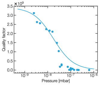
To quantify the effect of gas damping we performed ringdown measurements of the 3 cm nanomechanical resonator at different pressure levels and extracted the resulting quality factor from each dataset. The data points are then fitted using Equation S5 with and as fitting parameters. The result in Fig. S1 demonstrates that gas damping becomes negligible (less than 5%) for pressure levels approaching . The extracted quality factor equals the intrinsic value of 3.42 billion for this specific resonator. We therefore carried out all the measurements reported in the main text at this pressure level.
While the specific resonator employed for the pressure study hereby described is not the same device used for the results reported in Fig. 4 of the main text, the geometrical dimensions are equal. We can hence assume a similar gas damping behavior. Moreover Equation S5 has been developed for a beam with a uniform width, while the width of our resonators varies along its entire length due to the applied tapering and the PnC. One then has to resort to numerical simulations for an accurate calculation of the quality factor at every pressure level. However, the purpose of this study is to simply find the vacuum requirements to extract the intrinsic quality factor of the fabricated resonators not limited by gas damping, rather than accurately capturing the gas damping behavior. For this purpose, Equation S5 provides an accurate lower estimate.
.2 Variation of quality factor as function of thickness
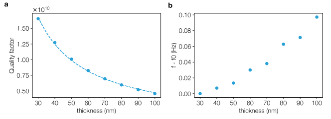
The predicted Q factor of the optimized centimeter-scale nanomechanical resonators is 10 billion, while the fabricated structures show a Q factor of 6.6 billion. We believe the observed difference is caused by difficulties to dissipate heat during the undercut process caused by the high-aspect-ratios. This results in different thicknesses and dimensions from edge to center along the beam of the fabricated nanostructures, with a significant effect on the measured Q factor.
In this section, we investigate the case for which the thickness of the Si3N4 layer is uniformly larger than the expected thickness, a value compatible with the etch settings employed during the undercut in view of the Si3N4 etch rate in SF6 plasma etching and the temperature of the process.
This thickness variation results in a reduction of the quality factor from over 1 billion at to at , as shown in Fig. S2a. This value is in good agreement with the value experimentally measured (Fig. 4a of the main text) of . On the contrary, the thickness has a negligible effect on the resonance frequency value as displayed in Fig. S2b, where is the resonance frequency obtained for the -thick resonator, corresponding to . This value agrees with experiments to around 1%, further confirming the high-fidelity between simulations and experiments.
.3 Stitching errors in electron beam lithography
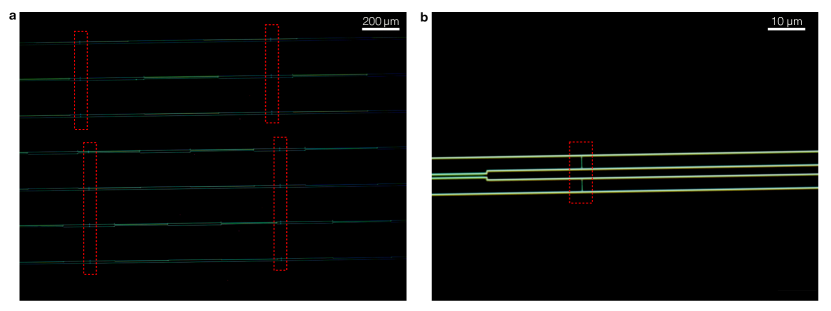
A pattern in electron beam lithography is generated by deflecting the electron beam based on the desired shape. However, due to the finite sweep range of the deflector system, the writing field cannot exceed an area of typically - . The maximum writing field for the Raith EBPG 5200 machine at Kavli Nanolab in Delft is . Large patterns need therefore to be stitched together by moving the sample on a stage. Misalignment between multiple writing fields might then arise due to miscalibration and thermal drift among other reasons. The consequent stitching errors have significant effects on the obtained shape. This is particularly relevant for high stress Si3N4, where a misalignment of the order of nanometers can lead to stress concentration and rupture of the fragile suspended structure.
The centimeter-scale nanomechanical resonators hereby developed require 30 writing fields to be correctly patterned by electron beam lithography. In order to accurately transfer the desired shape, we employed an electron beam with an estimated spot size equal to and a spacing of . The fine resolution results in a long writing time exceeding one hour, which increases the likelihood of misalignment and consequent stitching errors. For most of the exposed devices we in fact observed an incorrect patterning at the boundary of every writing field as shown in the dark-field microscope picture in Fig. S3a. Figure S3b provides a picture with higher magnification of the same structure which clearly shows a discontinuity of the written pattern.
In order to mitigate the observed stitching errors we focused first on reducing the long writing time. We did so by performing multiple exposures with different resolutions. The most critical features were exposed with a fine electron beam and high resolution, while a coarse electron beam with lower resolution was employed for the remaining areas of the pattern. As a result, the total writing time for a single nanomechanical resonator was reduced down to 10 minutes without affecting the accuracy of the desired pattern. This was effective to eliminate the systematic misalignment previously present at every writing field boundary (Fig. S3a), however, some stitching errors could still be observed in a random manner, varying from run to run.
To this end, we changed the dose at different positions to take into account possible underdose at the boundary between writing fields and overlapped each writing field with the nearby one for . This resulted in a correct exposure of the desired pattern, without any noticeable stitching error, and an accurate transfer of the centimeter-scale nanoresonators geometry.
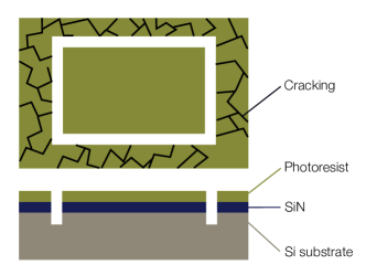
.4 Photoresist cracking at cryogenic temperature
Cryogenic deep reactive ion etching (DRIE) is employed in the fabrication of the centimeter-scale nanoresonators to increase the gap separating the suspended Si3N4 from the supporting Si substrate. Contrary to other deep silicon etching techniques as the Bosch process, cryo-DRIE is known to result in a smoother sidewall 69, and it does not leave carbon residues on the sidewall. In fact, the oxide passivation layer created to anisotropically etch Si dissolves at high temperatures. At the same time, its main drawback is the vulnerability of photoresists to cracking at low temperatures.
Previous studies found that cracking depends on the layer thickness and the specific photoresist material. The thin photoresist of less than are in fact reported to be free from cracking. Moreover, materials with a high degree of cross-linking and high mechanical strength do not suffer from cracking even for larger thickness. We then studied the effect of cryo-DRIE on the photoresist SU1813, spin coated on Si3N4 chips with thickness varying from to , before being exposed to the fluorine-based cryo-DRIE. The thickness is varied within an interval which provides enough material to obtain the desired gap size due to the photoresist selectivity. The thicker photoresist () shows cracks over the entire surface (Fig. S4c), while in the thinner photoresist () the cracks are localized at the outer area of the chip (Fig. S4b), in good agreement with the expected behavior. The cracks for the outer area of the thin photoresists are most likely caused by the non-uniform thickness at the edge, as Fig. S4a shows. We repeated the analysis for a second photoresist, AZ5214, without noticing any significant difference.
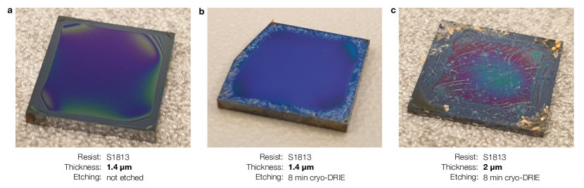
We therefore focused on a photoresist thickness of (Fig. S4b) in which the central area remains intact. Despite most of the surface being free from cracking, we observed that some cracks might propagate from the outer area towards the center with fatal consequences on the nanoresonators. Figure S5a shows an example where the cracks propagate toward the nanomechanical resonators area. The cracked resist patterns can then transfer into the underneath Si3N4 during etching, destroying the devices. A post-baking step of 15 minutes at prior to the etching was found to be effective to improve the photoresist plasma resistance and to further to reduce the cracks on the surface, but not to completely remove them. We also investigated the effect of the carrier wafer thickness and the Si substrate thickness. Previous studies found in fact that photoresist cracking is initiated by wafer deformation caused by the helium backside cooling system and can be mitigated by employing a thicker substrate 66. However, in our case, the photoresist cracking did not show any dependence on the substrate thickness.
We therefore surrounded the nanomechanical resonator’s area of the device with a protecting outer ring (Fig. S6). This ring is etched into both the Si3N4 layer and the upper part of Si substrate in order to create a physical barrier. The resulting pattern is shown in S5b which clearly shows the effectiveness of the developed method to prevent any cracks from propagating toward the nanomechanical resonators. It is nevertheless important to notice that often photoresist cracking was confined to the outer area of the device without propagating toward the central area (S5c),
.5 Beams collapsing
The centimeter-scale nanomechanical resonators are suspended by a fluorine based plasma etching performed at cryogenic temperature. The etching allows a quick and controllable release of the Si3N4 layer, without limitations from surface tension. However, plasma etching introduces charging effects due to the insulating nature of Si3N4. The charged Si3N4 can then be attracted by the Si substrate leading to the collapse of the nanoresonators.
Depending on the distance between the suspended resonator and the surrounding, we observed the Si3N4 being attracted toward or the side (Fig. S7c) or the bottom (Fig. S7b) of the opening around it. It follows that controlling the gap distance is an effective way to mitigate the collapse of the structures.
The distance from the wall along the in-plane direction can easily be controlled lithographically during the electron beam exposure. We observed that an opening larger than is needed to eliminate the probability of sticking to the wall. This affects the exposed area and thus the total writing time, which in turn can increase the probability of stitching errors. However as discussed in section .3, a multi exposure with different resolutions is an effective solution to reduce the total writing time and eliminate stitching errors.
On the other hand, the distance between the suspended resonator and the Si substrate along the out-of-plane direction needs to be controlled by an etching step. To this end, we performed a cryo-DRIE of the Si substrate prior to the release step. A gap under the suspended Si3N4 larger than was observed to be needed to avoid the collapse of the structure. The final pattern used in the main text has then a distance between the resonator and the wall of around , while the gap under the Si3N4 after the cryo-DRIE is of (Fig. S7a) .
.6 Optothermal effects on the measured Q factor
The quality factor of the fabricated centimeter-scale resonators is experimentally measured with the ringdown method. The resonator is mechanically excited close to resonance with a sinusoidal function before turning off the excitation and measuring the decay time. A linear fit in the logarithmic scale of the observed decay allows us to extract the decay rate and thus the quality factor. It is however of paramount importance to avoid any unintentional excitation of the resonator during the measurement to extract the correct value of the quality factor.
One possible source of unintentional excitation is the laser employed to interferometrically probe the displacement of the resonator. The optical power impinging on the suspended resonator can in fact optothermally or optically drive it. To address this issue, we employed a laser operating at , the wavelength at which Si3N4 has negligible absorption. Moreover, we minimized the laser power coupling to the resonator down to . This value is several orders of magnitude lower than the laser power conventionally used in previous studies (see for example 28), where no effects correlated to optothermal or optical excitation were observed. To further dismiss any contributions we performed different ringdown measurements by varying the laser power incident on the resonator from to . The results in Fig. S8 show a comparable decay rate for all the traces, suggesting that optothermal or optical effects are indeed negligible. The measurements are performed on the optimized design reported in the main text in Fig. 4.
.7 Multi-fidelity Bayesian optimization
The pursuit of efficient optimization of data scarce and high-fidelity black-box functions has led to Bayesian optimization techniques. These are statistical methods that yield a belief model over the entire domain which is sequentially updated through newly acquired data. The generic Bayesian optimization (BO) algorithm was originally introduced by Jones et al. 70, and is a proxy-optimization scheme: instead of optimizing directly over , one first selects a regressor to model the response surface based on a design of experiments , which is simply a set of known input-output pairs. Importantly, the response surface also includes a measure of uncertainty on top of the predicted outcome. This is why BO is often performed with Gaussian process regression (GPR) 71, 72, 73. Based on this regression model , a so-called acquisition function is built and optimized over the same domain. The goal of this proxy optimization is to suggest a new point in to be sampled with , and as such, the design of experiments is augmented with . In an algorithmic format, this can be expressed as follows:
Given the scarcity of high-fidelity data, a standard solution is to acquire higher-throughput data with lower fidelity, i.e., with larger uncertainty with lower cost. This context of simultaneous high- and low-fidelity data structures, combined with the ideas of GPR, gives rise to a multi-fidelity data driven modelling paradigm. The first multi-fidelity GPR (MFGPR) method was introduced by Kennedy & O’Hagan 74, under the term cokriging. Numerous other MFGPR methods have been constructed and researched since then 75, 76, 77, reviewed by Liu et al. 78.
There are several ways in which Bayesian optimization (Algorithm 1) can be extended to handle regressors over data sets with multiple fidelities, as is the case with MFGPR. A straightforward way can be described as follows, when the m indicates the function’s fidelity:
Note that this algorithm updates Algorithm 1, so that the acquisition function samples from both the fidelity function.
Interfacing MFGPR with BO has been discussed in practice by Forrester et al. 79 and Huang et al. 80 While the former simply applied expected improvement (EI) acquisition on the prediction of a single-fidelity, the latter devised an augmented version of EI. This acquisition function multiplies the EI function applied to the highest fidelity, with fidelity-dependent parameters such as the ratio of computational cost and correlation between the highest fidelity and the fidelity in question. This effectively separates the design space and fidelity space aspects of the multi-fidelity problem. More recently, Jiang et al. 81 have applied a similar multiplicative factor principle to create variable-fidelity upper confidence bound (VFUCB).
To demonstrate the process outlined by Algorithm 2, we use cokriging as the regressor along with VFUCB as the 2-fidelity () acquisition function (acq). See Fig. S9 for visualization in the case of multi-fidelity data sampled from the high- and low-fidelity Forrester functions 79, a set of similar one-dimensional objective functions.
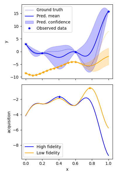
From Figure S9, the following can be inferred:
-
•
The maximum acquisition value of the low-fidelity branch is higher than that of the high-fidelity acquisition. Therefore, the fidelity selection is made in step 3 of Algorithm 2.
-
•
Compared to the maximizer of the high-fidelity acquisition branch, the maximizing -value of the low-fidelity branch is closer to the minimizing -value of the high-fidelity objective; the low-fidelity data is able to guide the optimization process.
.8 Multi-fidelity Bayesian optimization initial random points dependency
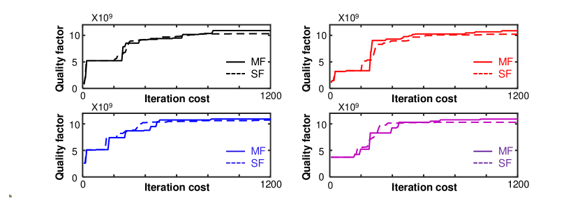
Since our simulation-based design problem handles a stochastic optimization on the beam-like nanomechanical resonator, the initial design of experiments affects the convergence to the optimum solution. The resonator has a design space with nine design parameters, making the initial points (25) affect the performance. Because we use multi-fidelity Bayesian optimization to reduce the total number of simulation evaluations, the curse of dimension is inevitable. Figure S10 shows the optimization history when we start from four different sets of random initial points. The change of initial points affects the convergence speed as expected, along with different behavior in selecting the fidelity. However, the optimized design obtained for all cases has converged on a similar design by taking advantage of the multi-fidelity optimization.
.9 PnC beam resonator’s design parameters
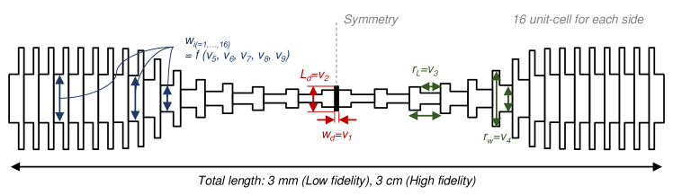
The one dimensional PnC resonator has a total length of (or ) length with a total of 32 unit cells. During the Bayesian optimization, the quality factor of the resonator is maximized by changing nine design parameters. Figure S11 illustrates the design parameters of the optimized resonator discussed in the manuscript. Two parameters correspond to the defect’s width () and length () in the bound of [, ], [, ] ([, ]), respectively. Two parameters illustrate the width () and the length() ratio for each of the unit-cell in the bound of , , respectively. The width ratio is the ratio between the wide and thin parts of the unit cells, and the length ratio is the ratio between the length of the thin part of the unit cell versus the total length of the unit cells. The tapered shape was defined by five design parameters in the bound of [, ]. We performed Piecewise Cubic Hermite Interpolating Polynomial for the 16 unit-cell’s width of the thin part on the shape-determinating design parameters. The simulation was performed to find the maximum quality factor in the range of 100 kHz to 400 kHz, considering the defect mode using the bandgap. The length of the unit cells was determined considering the bandgap frequency matching condition, once the set of each unit cell’s width is defined30. During the optimization, the resonator’s thickness was set to 50 nm.