Field-Emission Resonances in Thin Metallic Films: Nonexponential Decay of the Tunneling Current as a Function of the Sample-to-Tip Distance
I Abstract
Field-emission resonances (FERs) for two-dimensional Pb(111) islands grown on Si(111)77 surfaces were studied by low-temperature scanning tunneling microscopy and spectroscopy (STM/STS) in a broad range of tunneling conditions with both active and disabled feedback loop. These FERs exist at quantized sample-to-tip distances above the sample surface, where is the serial number of the FER state. By recording the trajectory of the STM tip during ramping of the bias voltage (while keeping the tunneling current fixed), we obtain the set of the values corresponding to local maxima in the derived spectra. This way, the continuous evolution of as a function of for all FERs was investigated by STS experiments with active feedback loop for different . Complementing these measurements by current–distance spectroscopy at a fixed , we could construct a 4-dimensional diagram, that allows us to investigate the geometric localization of the FERs above the surface. We demonstrate that (i) the difference between neighboring FER lines in the diagram is independent of for higher resonances, (ii) the value decreases as increases; (iii) the quantized FER states lead to the periodic variations of as a function of with periodicity ; (iv) the periodic variations in the spectra allows to estimate the absolute height of the tip above the sample surface. Our findings contribute to a deeper understanding on how the FER states affect various types of tunneling spectroscopy experiments and how they lead to a non-exponential decay of the tunneling current as a function of at high bias voltages in the regime of quantized electron emission.
∗ Corresponding author, e-mail address: aladyshkin@ipmras.ru
II Introduction
An appearance of surface electronic states localized near flat surfaces of crystals was predicted theoretically by Tamm Tamm-JETP-32 in the tight-binding model and later by Goodwin Goodwin-Proc-35 and Shockley Shockley-JETP-39 within the nearly-free-electron approximation. It was demonstrated that the discontinuity of the potential energy at the crystalline surface could generate stationary localized solutions of the Schrödinger equation corresponding to exponentially decaying wave functions both in vacuum above the sample surface and in the bulk below the sample surface (with atomic-scale oscillations). A review of various methods of theoretical analysis of surface electronic states is presented in Ref. Davison-book .
Rather than a discrete discontinuity, in reality the electric potential above the metallic crystal surface has a slowly decreasing component (, where is the distance from the metal-vacuum interface) because of the electrostatic Coulomb interaction between the probe electron and its mirror (image) charge (see, e.g. Book-Electrodynamics-1 ; Book-Electrodynamics-2 ). The appearance of the Coulomb-like potential could lead to the localization of electrons above the surface of conducting sample provided that the energies of these states correspond to the forbidden band of bulk crystal. The effect of trapping of electrons above the flat surface is similar to the localization of electrons in hydrogen-like atoms, and therefore it leads to a Rydberg-like spectrum of excitations (see reviews McRae-RMP-79 ; Echenique-review-1 ; Echenique-review-2 and references therein). In literature these electronic states are known as image-potential states (IPSs), although from physical point of view these states can be considered as a generalization of the Tamm-Shockley surface states for the case of continuously varied electrical potential near the surface, what results in a shift of the oscillatory part of the wave function outside the sample (figures S1 and S2 in Supporting Information). IPSs in the absence of external electric field are usually studied by means of photoemission spectroscopy Garcia-PRL-85 ; Hofer-Science-97 .
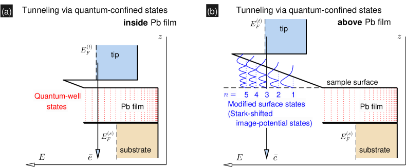
The effect of quasi-stationary electronic states localized above a surface of conducting samples on transport properties of quantum-confined system becomes more pronounced in the presence of external sources of electric field. This configuration is typical for scanning tunneling microscopy (STM) and spectroscopy (STS). Indeed, for a non-zero tunneling voltage (bias) between a STM tip and a sample the effective electric potential near the surface can be viewed as a superposition of the Coulomb potential of the image charge and the linearly increasing function of . Obviously, the positions of all modified surface states in the presence of the external electric field are shifted upward to higher energies Binnig-PRL-85 similar to the Stark effect for a hydrogen-like atom Landau-III . The wave functions corresponding to the modified surface states in linearly increasing electric potential are shown schematically in figure 1b. The influence of the quantized electronic states localized within potential barrier area on the energy dependence of the transmission coefficient for the trapezoidal tunneling barrier and on the current-voltage () dependence were theoretically considered by Gundlach Gundlach-SolStateElectr-66 . Sometimes the oscillations of the differential conductance as a function of conditioned by resonant tunneling via the modified surface states are referred to as the Gundlach oscillations or field-emission resonances (FERs). The FERs were experimentally studied for atomically flat surfaces Becker-PRL-85 ; Bobrov-Nature-01 ; Wahl-PRL-03 ; Jung-PRL-95 ; Hanuschkin-PRB-07 ; Kubetzka-APL-07 ; Silkin-PRB-09 ; Jarvinen-JPCC-2015 ; Martinez-Blanco-PRB-15 ; Ge-PRB-20 ; Borca-2D-20 ; and for various nanostructured objects on top of flat surfaces Borisov-PRB-07 ; Rienks-PRB-05 ; Dougherty-PRL-06 ; Pivetta-PRB-05 ; Ploigt-PRB-07 ; Lin-PRL-07 ; Aladyshkin-JPCM-20 ; Konig-JPCC-09 ; Schouteden-PRL-09 ; Liu-Nanolett-21 ; Stuckenholz-JPCC-15 ; Schouteden-PRL-12 ; Yang-PRL-09 ; Becker-PRB-10 ; Schouteden-Nanotech-10 ; Craes-PRL-13 ; Sugawara-PRB-17 ; Park-JPCC-12 . In particular, the analysis of the spectra of the FERs allows to estimate the local work function Pivetta-PRB-05 ; Ploigt-PRB-07 ; Lin-PRL-07 ; Aladyshkin-JPCM-20 ; Konig-JPCC-09 ; Stuckenholz-JPCC-15 ; Liu-Nanolett-21 ; Kolesnychenko-RSI-99 ; Kolesnychenko-PhysB-00 and to probe the profile of surface potential Bono-SurfSci-87 ; Ruffieux-PRL-09 .
In this paper we study geometric localization of FERs for thin Pb(111) films on Si(111) surfaces by means of low-temperature STS in the regime of constant tunneling current and variable distance between the STM tip and the Pb surface. The main aim of the paper is to demonstrate that the FERs affect strongly the current–distance () relationship, resulting in periodic variations in the logarithmic derivative of with respect to (i.e. ) as a function of for a fixed tunneling voltage. This observation apparently differs from well-known exponential-like dependences of the tunneling current as a function of the width of the low-transmission potential barrier in the limit of low and high voltages. Indeed, the dominant contribution to for planar contacts at large distances is controlled by the mean work functions of the sample and the tip Holm ; Simmons-1 ; Simmons-2
| (1) |
or by the work function of the tip Holm ; Simmons-1 ; Simmons-2
| (2) |
Here and are mass and charge of electron in a vacuum spacer, is the mean bias voltage, and are work functions for the sample (collector of electrons) and the tip (emitter of electrons). Important to note that both estimates (S5) and (S9) are independent on , what should correspond to universal linear decrease of as function of regardless on the bias. However we find out that trivial exponential decay of tunneling current or, equivalently, linear decay of as a function of for large bias voltage is substantially modified in the regime of quantized electronic emission. We determine the set of quantized heights and energies , corresponding to the local maxima of , that are related to the FER states, where is the serial number of the resonance. We argue that the period of the oscillations of the logarithmic derivative of the tunneling current is independent on and monotonously decreases as increases. To the best of our knowledge, such bias-dependent periodic oscillations of as a function of in STS experiments have not been yet discussed in literature. Our experimental findings can be interpreted within the quasi-classical model for electron trapped in the triangular potential well. Based on our experiments and analysis, we can state that similar effects controlled by resonant tunneling through quasi-stationary states above the sample surface should exist for any conducting material provided that the STM tip has a proper shape.
(b) Typical dependence of on the bias potential , acquired for pA at the point .
III Methods
Experimental investigations of electrophysical properties of quasi-two-dimensional Pb islands were carried out in an ultra-high vacuum (UHV) low-temperature scanning probe microscopy setup (Omicron Nanotechnology GmbH) operating at a base vacuum pressure mbar. Si(111) crystals were first out-gassed at about 600∘C for several hours then cleaned in-situ by direct-current annealing at about 1300∘C, resulting in formation of reconstructed Si(111)77 surface. Thermal deposition of Pb (Alfa Aesar, purity of 99.99%) from a Mo crucible was performed in-situ on Si(111)77 surface at room temperature by means of an electron-beam evaporator (Focus GmbH, model EFM3) at mbar. The orientation of the atomically flat terraces at the upper surface of the Pb islands corresponds to the (111) plane Altfeder-PRL-97 ; Su-PRL-01 ; Eom-PRL-06 . All STM/STS measurements were carried out at liquid nitrogen temperatures (from 78 to 81 K) with electrochemically etched W tips cleaned in-situ by electron bombardment. To optimize the shape of the STM tip apex after the cleaning, we touch the surface of clean Pb terraces by changing the distance between the tip and the sample surface from zero (actual position) to nm (well below surface). We can therefore assume that our W tips become covered by a Pb layer during our series of experiments. The lateral and vertical thermal drifts of the piezo-scanner after thermal stabilization are less than 0.5 nm/hour.
The topography of the Pb islands was studied by low-temperature STM by tracking the displacement of piezoscanner during scanning along the sample surface with active feedback loop (constant tunneling current ) and constant electrical potential of the sample () with respect to a virtually grounded STM tip (). In order to study the variations of the electronic properties of the sample at sweeping we use the following measurement protocol Schouteden-PRL-09 ; Schouteden-PRL-12 ; Schouteden-Nanotech-10 ; Aladyshkin-JPCM-20 . First, we adjust the initial height of the tip above the sample surface by varying the set-point value at a nonzero . We would like to note that the absolute value of the initial height is unknown. Next, we ramp the tunneling voltage for fixed lateral coordinates of the tip, keeping the tunneling current equal to . Typical acquisition time for a single spectroscopic measurement is 40 sec. During ramping, we record output signal of the active STM feedback loop (in Volts). The acquired data can be transformed in so-called distance-voltage () spectra: dependences of the relative height in nanometers on , where nm/V is the conversion factor for our piezo-scanner at 78 K. We smooth the dependence using a Gaussian filter with a window of 20 mV to remove high-frequency noise and then numerically calculate the rate of the height variation as a function of or given .
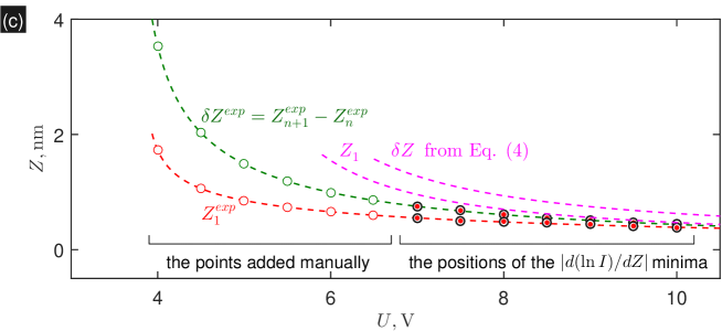
(b) The dependence of on (solid black line) at V, the dashed line is the linear extrapolation for this dependence towards higher values. Black circles in the panels (a) and (b) indicate the values corresponding to the local minima in the dependences on , where is the number of the FER, is the bias-dependent period of the oscillations of . Red dots in the panels (a) and (b) are the estimated positions of the local minima of .
(c) The dependences of on (red dashed line) and on (green dashed line), obtained by fitting of the experimental data shown in the panel a. For the WKB model we use Eq. (4) taking into account and eV.
IV Results and discussion
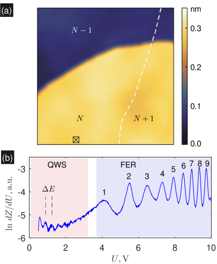
Figure 2a shows the topography image of the Pb(111) island with two flat terraces on the upper surface. This image indicates the absence of visible and hidden defects in the vicinity of the point , where the local tunneling spectra were recorded.
The typical dependence of the rate of the height variations on is shown in figure 2b. Periodic small-scale oscillations on the dependence at low bias voltage (V) can be considered as clear experimental evidence for the coherent resonant tunneling through quantum-well states (QWSs) in the thin metallic film Ustavshchikov-JETPLett-17 ; Altfeder-PRL-97 ; Su-PRL-01 ; Eom-PRL-06 ; Hong-PRB-09 (see schematics in figure 1a). Taking the period of the quantum-size oscillations eV, one can estimate the local thickness nm with respect to the Si(111) surface using the relationship , where cm/s is the Fermi velocity for the Pb(111) films Ustavshchikov-JETPLett-17 ; Altfeder-PRL-97 .
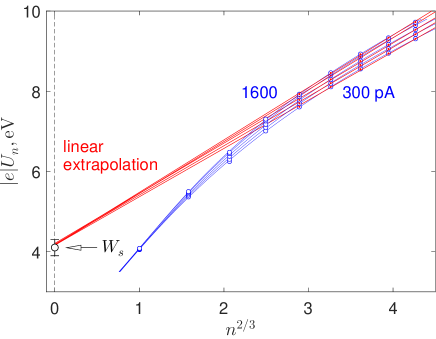
Aperiodic large-scale oscillations on the dependence on clearly visible in figure 2b at high bias voltage (V) point to FERs, conditioned by the coherent resonant tunneling through the surface electronic states (see schematics in figure 1b). Figure 3 shows the voltage positions of the FER as a function of extracted from the dependence of on for different measuring current , where is serial number of FER. One can see that the increase in systematically shifts all the FERs to higher values. The evolution of the resonant energies at varying , and local electric field can be interpreted in terms of the quasi-classical model based on the Wentzel-Kramers-Brillouin (WKB) approximation for the electron localized in the triangular potential well (see Supporting Information). This model makes it possible to estimate the resonant bias values corresponding to the higher-order FER states Aladyshkin-JPCM-20
| (3) |
where , is a constant, is the gradient of the potential energy for electron above the sample surface, is the Volta contact potential, is the local electrical field, is the width of the trapezoidal potential barrier (i.e. the distance between the STM tip and the sample surface). It is important to note, that this expression (3) is identical to that derived for the positions of the maxima for the tunneling junction with trapezoidal potential barrier between two metals in the free-electron-gas approximation Kolesnychenko-PhysB-00 .
Considering expression (3) and keeping in mind that for , we conclude that
(i) the difference is proportional to the product of and . Since the increase in the measurement current results to the decrease in the starting height and, correspondingly, the increase in the local electric field , it should cause the shift of to the higher values. This conclusion is in the agreement with our findings (figure 3).
(ii) the extrapolation of the linear fitting function for the dependence on for the higher-order FER states towards the point should give a reasonable estimate for the work function regardless of . This approach was already used for estimating the work functions for Ag and Co nanoislands Lin-PRL-07 , Pb films Aladyshkin-JPCM-20 and Pt wires Kolesnychenko-PhysB-00 . Analysing the data in figure 3, one can see that the linear asymptotes of the dependences on for the high- limits for different intersect the axis of ordinates at the same point. It gives us the reasonable estimate for the local work function eV for this particular Pb film independently on the measurement current.
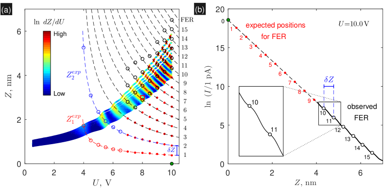
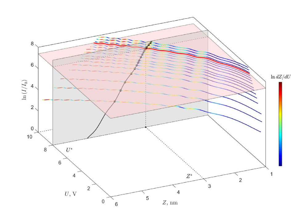
In order to study the geometrical localization of the FER we compose a 3-dimensional diagram that is based on individually recorded spectra at various tunneling currents (figure 4a). To minimize any effect of thermal drift in the vertical direction and the vertical creep of the piezo-scanner, caused by repeating procedures of approaching/retraction of the tip, we propose the following original method of the mutual adjustment of the series of the dependences of on acquired for the given current and the series of the dependences of on acquired for the given voltage. We would like to emphasize that the distance is measured from the actual position of the tip above the sample, so the absolute height of the tip above the sample surface remains unknown. Since the typical width of the here investigated atomically flat Pb(111) terraces (nm in the area of interest, see Fig. 1) is much larger than the lateral displacement of the tip during local spectral measurements (nm), the lateral thermal drift can be considered as non significant for our experiments. Experimental confirmation of the independence of the FER spectrum on the tip position for the Pb(111) films (except the edges of the monatomic steps) is presented in Aladyshkin-JPCM-20 .
First, we choose the parameters , , and assign the value to the actual height measured at and . For example, the diagram in figure 4a is composed for arbitrary-chosen values V, pA and nm. Second, we record the dependence at and plot this line in the diagram in such a way that this calibration curve runs through the chosen point ). Third, we record the dependence at . Thus, these two reference curves form a frame for the consistent visualization for the rest of the measured data in a four-dimensional space of parameters (figures S3 and S4 in Supporting Information). Fourth, we acquire the series of the dependences on at and plot them in the pseudo-color manner choosing the color of each point proportional to . We check that any change in the parameters , and used for the adjustment does not result in a modification of the composed diagram except the distortion-free shift of this diagram in the vertical direction depending on the particular value.
The most remarkable feature of the diagram presented in figure 4a is the well-defined stripe-like structure. Apparently, for given bias voltage (V) one can determine the set of the widths of the trapezoidal potential barrier in such a way that the energy of the th resonant electronic state in the triangular well will be close to the Fermi level of the tip (see figures S5 and S6 in Supporting Information). Under this condition the electrons from the tip start to tunnel to the sample by a resonant manner, what should lead to the increase in the tunneling current for the considered quantum system. However in our case the active feedback loop immediately retract the tip from the surface in order to keep the current, what results in the rapid variations of the height at upon sweeping . It explains why blue and red stripes in the diagram do relate to the FER states. The number of the visible stripes on the diagram depends on the shape of the tip (not shown in this paper), since the latter affects the profile of the triangular potential well. Interestingly that the absolute value of the slope of the red stripes in figure 4a (i. e. for constant ) monotonously decreases as increases.
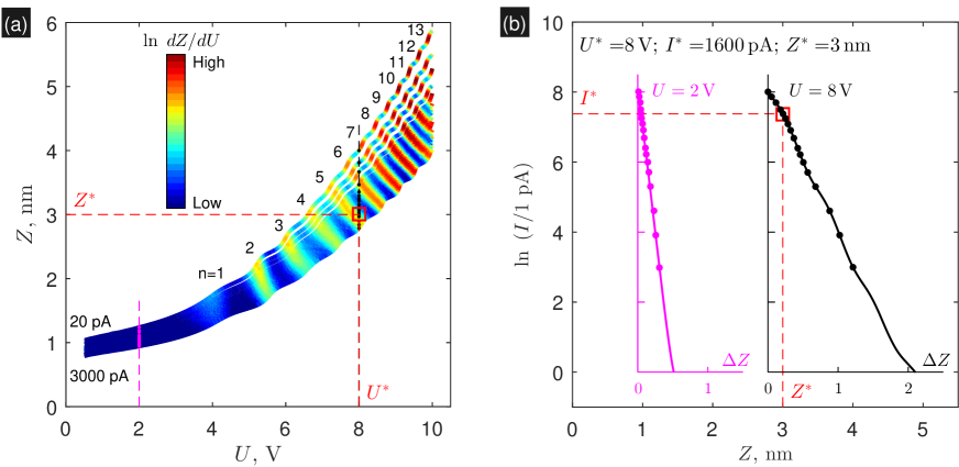
We would like to emphasize that the dependence of on could deviate from a linear decreasing function. Indeed, at high bias voltage one can see the pronounced periodic oscillations of the local slope as a function of . The positions of the minimal values are marked by black circles in figure 4b. By extrapolating the dependence of on to higher values and using the estimated period of the oscillations for the high resonances, one can determine the expected positions of the oscillations conditioned by the low resonances (red dots in figure 4b). We carry out this procedure for the dependences of on in the range 7 VV, where the periodic oscillations of the local slope are clearly visible, and thus the estimates of their periods are reliable. We mark the positions of the minimal values (both observed and expected) on the diagram (figure 4a). In order to explain the periodic variations of the local slope, we rewrite Eq. (3) in the following form
| (4) |
thus expressing the quantized heights as a function of and . It is easy to see that in the considered model all dependences on have the universal vertical asymptote at . According to Eq. (4), the difference between two adjacent values depends only on ( for ) and independent of (see purple dashed line in figure figure 4c and figure S6 in Supporting Information). The independence of on is in agreement with our experimental findings (figure 4a). Indeed, using two bias-dependent functions and (red and green dashed lines in figure 4c), we can correctly describe the positions of all FERs on the diagram using simple relationship: , where We conclude our simple WKB-based model correctly describes the evolution of the experimental dependences and from qualitative and quantitative (at high values) points of view.
(b) Dependences of the local slope on for in the range from 6 to 10 V (from bottom to top); all the curves are shifted vertically for clarity.
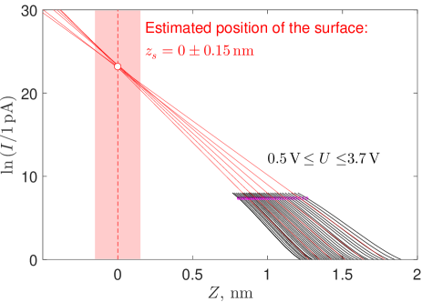
The observed oscillatory dependence of on makes it possible to estimate the absolute position of the STM-tip above the sample surface in a non-destructive way. Indeed, by subsequent measurements of both the dependence (at constant current) and the dependence (at constant high tunneling voltage) one can determine the quantized heights by analyzing the variation of the slope in the dependence (figure 4b) and unambiguously assign the proper indices to all FER states. The extrapolated position of the zero-order FER (green dot in figures 4a,b) yields the estimate of the z-coordinate of the sample surface. From our analysis we choose the parameter to be equal to 3 nm, since this value corresponds to the surface positioned at . An alternative way to estimate the absolute position of the sample surface is presented in figure 5. This method is based on a linear extrapolation of the dependences of on for tunneling voltages below the work function to avoid the mentioned oscillations of the local slope. We find that all extrapolated functions intersect at the same point. This point can be considered as an indication for the position of the surface where a virtual electric contact takes place. Interestingly, both approaches yield the same value: . We note that, in our opinion, the accuracy of both approaches cannot be better than the typical size of the Pb atom, which is of the order of the covalent radius (0.15 nm).
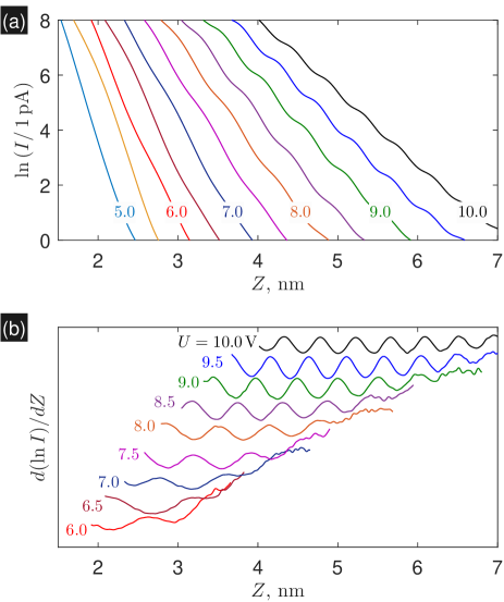
Figure 6 illustrates the effect of the FERs on the current-distance dependences, which we can now understand from the analysis discussed above: (i) the appearance of the periodic oscillations on the dependence of on at high tunneling voltage and (ii) the decrease in the period of the oscillations at increasing . It should be emphasized that the dependences of on (figure 6a), used for numerical calculation of as a function of (figure 6b), are acquired directly by means of current-distance spectroscopy without the complicated procedure of mutual alignment of the spectroscopic data. It demonstrates to that the oscillatory behaviour of as a function of is a real physical effect inherent for all conducting samples in the field-emission regime and it cannot be considered as an artifact of data analysis. The effect of the shape of the STM tip on the period of these oscillations will be the scope of our further investigation.
V Conclusion
We experimentally studied the field-emission resonances for electrons above Pb(111) films by means of low-temperature scanning tunneling spectroscopy for a broad range of tunneling conditions. The field-emission resonances can be recognized as local maxima in the dependence of the rate of the height variations on the tunneling voltage for given . Repeating single-point spectroscopical measurements for values, we composed hyperbolic-like lines on the diagram illustrating the dependence of the quantized heights on , where is the serial number of the field-emission resonance. We argued that the field-emission resonances strongly affect the dependence of on for given (so-called current-distance dependence). In particular, the field-emission resonances results in nonlinear oscillatory decay of and, correspondingly, non-exponential decrease of as a function of for constant bias values exceeding the sample work function.
VI Acknowlednements
The authors are grateful to S. I. Bozhko and A. S. Mel’nikov for valuable comments. The work was performed with the use of the facilities at the Common Research Center ’Physics and Technology of Micro- and Nanostructures’ at Institute for Physics of Microstructures RAS and funded by the Russian State Contract (No. 0030-2021-0020).
VII Supporting Information Available
Additional figures illustrating the principle of mutual adjustment of the tunneling spectra as well as spatial structures of the wave functions for surface electronic states are presented in the Supporting Information.
REFERENCES
References
- (1) Tamm, I. Phys. Z. Sowjetunion. 1932, 1, 733.
- (2) Goodwin, E. T. Electronic states at the surfaces of crystals. Proc. Camb. Phil. Soc. 1939, 35, 205.
- (3) Shockley, W. On the surface states associated with a periodic potential. Phys. Rev. 1939, 56, 317-323.
- (4) Davison, S. G.; Steślicka, M. Basic Theory of Surface States. Clarendon Press, 1996.
- (5) Landau, L. D.; Lifshitz, E. M. Electrodynamics of Continuous Media, ed., London Elsevier, 1960.
- (6) Jackson, J. D. Classical Electrodynamics. John Wiley & Sons, 1962.
- (7) McRae, E. G. Electronic surface resonances of crystals. Rev. Mod. Phys. 1979, 51, 541-568.
- (8) Echenique, P. M.; Pendry J. B. The existence and detection of Rydberg states at surfaces. J. Phys. C: Solid State Phys. 1978, 11, 2065-2075.
- (9) Echenique, P. M.; Pendry J. B. Theory of image states at metal surfaces. Prog. Surf. Sci. 1990, 82, 111-172.
- (10) Garcia, N.; Reihl, B.; Frank, K. H.; Williams A. R. Image states: Binding energies, effective masses, and surface corrugation. Phys. Rev. Lett. 1985, 54, 591-594.
- (11) Höfer, U.; Shumay, I. L.; Reuß, Ch.; Thomann, U.; Wallauer, W.; Fauster Th. Time-resolved coherent photoelectron spectroscopy of quantized electronic states on metal surfaces. Science 1997, 277, 1480-1482.
- (12) Binnig, G.; Frank, K. H.; Fuchs, H.; Garcia, N.; Reihl, B.; Rohrer, H.; Salvan, F.; Williams, A. R. Tunneling spectroscopy and inverse photoemission: image and field states. Phys. Rev. Lett. 1985, 55, 991-994.
- (13) Landau, L. D.; Lifshitz, E. M. Quantum mechanics: non-relativistic theory. Pergamon Press, USA, 1977.
- (14) Gundlach, K. H. Zur berechnung des tunnelstroms durch eine trapezförmige potentialstufe. Solid-State Electr. 1966, 9, 949-957.
- (15) Becker, R. S.; Golovchenko, J. A.; Swartzentruber, B. S. Electron interferometry at crystal surfaces. Phys. Rev. Lett. 1985, 55, 987-990.
- (16) Bobrov, K.; Mayne, A. J.; Dujardin, G. Atomic-scale imaging of insulating diamond through resonant electron injection. Nature 2001, 413, 616-619.
- (17) Wahl, P.; Schneider, M. A.; Diekhöner, L.; Vogelgesang, R.; Kern, K. Quantum coherence of image–potential states. Phys. Rev. Lett. 2003, 91, 106802.
- (18) Jung, T.; Mo, Y. W.; Himpsel, F. J. Identification of metals in scanning tunneling microscopy via image states. Phys. Rev. Lett. 1995, 74, 1641-1644.
- (19) Hanuschkin, A.; Wortmann, D.; Blügel, S. Image potential and field states at Ag(100) and Fe(110) surfaces. Phys. Rev. B 2007, 76, 165417.
- (20) Kubetzka, A.; Bode, M.; Wiesendanger, R. Spin-polarized scanning tunneling microscopy in field emission mode. Appl. Phys. Lett. 2007, 91, 012508.
- (21) Silkin, V. M.; Zhao, J.; Guinea, F.; Chulkov, E. V.; Echenique, P. M.; Petek, H. Image potential states in graphene. Phys. Rev. B 2009, 80, 121408(R).
- (22) Järvinen, P.; Kumar, A.; Drost, R.; Kezilebieke, S.; Uppstu, A.; Harju, A.; Liljeroth P. Field-emission resonances on graphene on insulators. J. Phys. Chem. C 2015, 119, 23951-23954.
- (23) Martinez-Blanco J., Erwin, S. C.; Kanisawa, K.; Fölsch, S. Energy splitting of image states induced by the surface potential corrugation of InAs(111)A. Phys. Rev. B 2015, 92, 115444.
- (24) Ge, J.-F.; Zhang, H.; He, Y.; Zhu, Z.; Yam, Y. C., Chen, P.; Hoffman, J. E. Probing image potential states on the surface of the topological semimetal antimony. Phys. Rev. B 2020, 101, 035152.
- (25) Borca, B.; Castenmiller, C.; Tsvetanova, M.; Sotthewes, K.; Rudenko, A. N.; Zandvliet H. J. W. Image potential states of germanene. 2D Mater. 2020, 7, 035021.
- (26) Borisov, A. G.; Hakala, T.; Puska, M. J.; Silkin, V. M.; Zabala, N.; Chulkov, E. V.; Echenique, P. M. Image potential states of supported metallic nanoislands. Phys. Rev. B 2007, 76, 121402(R).
- (27) Rienks, E. D. L.; Nilius, N.; Rust, H.-P.; Freund, H.-J. Surface potential of a polar oxide film: FeO on Pt(111). Phys. Rev. B 2005, 71, 241404(R).
- (28) Dougherty, D. B.; Maksymovych, P.; Lee, J.; Yates Jr., J. T. Local spectroscopy of image-potential-derived states: From single molecules. Phys. Rev. Lett. 2006, 97, 236806.
- (29) Pivetta, M.; Patthey, F.; Stengel, M.; Baldereschi, A.; Schneider, W.-D. Local work function Moiré pattern on ultrathin ionic films: NaCl on Ag(100). Phys. Rev. B 2005, 72, 115404.
- (30) Ploigt, H.-C.; Brun, C.; Pivetta, M.; Patthey, F.; Schneider, W.-D. Local work function changes determined by field emission resonances: NaCl/Ag(100). Phys. Rev. B 2007, 76, 195404.
- (31) Lin, C. L.; Lu, S. M.; Su, W. B.; Shih, H. T.; Wu, B. F.; Yao, Y. D.; Chang, C. S.; Tsong, T. T. Manifestation of work function difference in high order Gundlach oscillation. Phys. Rev. Lett. 2007, 99, 216103.
- (32) Stuckenholz, S.; Büchner, C.; Heyde, M.; Freund, H.-J. MgO on Mo(001): Local work function measurements above pristine terrace and line defect sites. J. Phys. Chem. C 2015, 119, 12283-12290.
- (33) König, T.; Simon, G. H.; Rust, H.-P.; Heyde, M. Work function measurements of thin oxide films on metals – MgO on Ag(001). J. Phys. Chem. C 2009, 113, 11301-11305.
- (34) Aladyshkin, A. Yu.; Quantum-well and modified image-potential states in thin Pb(111) films: an estimate for the local work function. Journal of Physics: Condens. Matter 2020, 32, 435001.
- (35) Schouteden, K.; Van Haesendonck, C. Quantum confinement of hot image-potential state electrons. Phys. Rev. Lett. 2009, 103, 266805.
- (36) Schouteden, K.; Van Haesendonck, C. Lateral quantization of two-dimensional electron states by embedded Ag nanocrystals. Phys. Rev. Lett. 2012, 108, 076806.
- (37) Schouteden, K.; Volodin, A.; Muzychenko, D. A.; Chowdhury, M. P.; Fonseca, A.; Nagy, J. B.; Van Haesendonck, C. Probing quantized image–potential states at supported carbon nanotubes. Nanotechnology 2010, 21, 485401.
- (38) Yang, M. C.; Lin, C. L.; Su, W. B.; Lin, S. P.; Lu, S. M.; Lin, H. Y.; Chang, C. S.; Hsu, W. K.; Tsong, T. T. Phase contribution of image potential on empty quantum well states in Pb islands on the Cu(111) surface. Phys. Rev. Lett. 2009, 102, 196102.
- (39) Becker, M.; Berndt, R. Scattering and lifetime broadening of quantum well states in Pb films on Ag(111). Phys. Rev. B 2010, 81, 205438.
- (40) Craes, F.; Runte, S.; Klinkhammer, J.; Kralj, M.; Michely, T.; Busse, C. Mapping image potential states on graphene quantum dots. Phys. Rev. Lett. 2013, 111, 056804.
- (41) Sugawara, K.; Nagase, K.; Yamazaki, S.; Nakatsuji, K.; Hirayama, H. Interaction of Stark-shifted image potential states with quantum well states in ultrathin Ag(111) islands on Si(111)--B substrates. Phys. Rev. B 2017 96, 075444.
- (42) Park, J.; Ueba, T.; Terawaki, R.; Yamada, T.; Kato, H. S. and Munakata, T. Image Potential State Mediated Excitation at Rubrene/Graphite Interface. J. Phys. Chem. C 2012, 116, 5821-5826.
- (43) Liu, X.; Wang, L.; Yakobson, B. I.; Hersam, M. C. Nanoscale probing of image-potential states and electron transfer doping in borophene polymorphs. Nano Letters 2021, 21, 1169-1174.
- (44) Kolesnychenko, O. Yu.; Shklyarevskii, O. I.; van Kempen, H. Calibration of the distance between electrodes of mechanically controlled break junctions using field emission resonance. Rev. Sci. Instrum. 1999, 70, 1442.
- (45) Kolesnychenko, O. Yu.; Kolesnichenko, Yu. A.; Shklyarevskii, O. I.; van Kempen H. Field-emission resonance measurements with mechanically controlled break junctions. Physica B 2000, 291, 246-255.
- (46) Bono, J.; Good Jr., R. H. Conductance oscillations in scanning tunneling microscopy as a probe of the surface potential. Surf. Sci. 1987, 188, 153-163.
- (47) Ruffieux, P.; Ait-Mansour, K.; Bendounan, A.; Fasel, R.; Patthey, L.; Gröning, P.; Gröning O. Mapping the electronic surface potential of nanostructured surfaces. Phys. Rev. Lett. 2009, 102, 086807.
- (48) Holm, R. The electric tunnel effect across thin insulating films in contacts. J. Appl. Phys. 1951, 22, 569-574.
- (49) Simmons J. G. Generalized formula for the electric tunnel effect between similar electrodes separated by a thin insulating film. J. Appl. Phys. 1963, 34, 1793-1803.
- (50) Simmons J. G. Electric tunnel effect between dissimilar electrodes separated by a thin insulating film. J. Appl. Phys. 1963, 34, 2581-2590.
- (51) Altfeder, I. B.; Matveev, K. A.; Chen, D. M. Electron fringes on a quantum wedge. Phys. Rev. Lett. 1997, 78, 2815-2818.
- (52) Su, W. B.; Chang, S. H.; Jian, W. B.; Chang, C. S.; Chen, L. J.; Tsong, T. T. Correlation between quantized electronic states and oscillatory thickness relaxations of 2D Pb Islands on Si(111) surfaces. Phys. Rev. Lett. 2001, 86, 5116-5119.
- (53) Eom, D.; Qin, S.; Chou, M. Y.; Shih, C. K. Persistent superconductivity in ultrathin Pb films: A scanning tunneling spectroscopy study. Phys. Rev. Lett. 2006, 96, 027005.
- (54) Hong, I.-P.; Brun, C.; Patthey, F.; Sklyadneva, I. Yu.; Zubizarreta, X.; Heid, R.; Silkin, V. M.; Echenique, P. M.; Bohnen, K. P.; Chulkov, E. V. et al. Decay mechanisms of excited electrons in quantum-well states of ultrathin Pb islands grown on Si(111): Scanning tunneling spectroscopy and theory. Phys. Rev. B 2009, 80, 081409.
- (55) Putilov, A. V.; Ustavshchikov, S. S.; Bozhko, S. I.; Aladyshkin, A. Yu. Nonuniform quantum-confined states and visualization of hidden defects in Pb(111) films. JETP Lett. 2019, 109, 755-761.
- (56) Ustavshchikov, S. S.; Putilov, A. V.; Aladyshkin, A. Yu. Tunneling interferometry and measurement of the thickness of ultrathin metallic Pb(111) films. JETP Lett. 2017, 106, 491-497.
- (57) Aladyshkin, A. Yu.; Aladyshkina, A. S.; Bozhko, S. I. Observation of hidden parts of dislocation loops in thin Pb films by means of scanning tunneling spectroscopy. J. Phys. Chem. C 2021, 125, 26814-26822.
SUPPORTING INFORMATION
Quantum-confined states in a one-dimensional potential well
It is illustrative to consider a model problem describing the formation of localized electronic states in one-dimensional (1D) potential well
| (S5) |
where and are the eigenfunctions and the eigenvalues of the Schrödinger equation (S5) and is the potential energy. For simplicity we take the periodic potential inside the quantum well in the form of a combination of two Fourier components
| (S9) |
where is the lattice parameter and is the width of the quantum well. Two Fourier-components of the potential ensure the formation of two forbidden gaps in the spectrum of the electronic eigenstates.
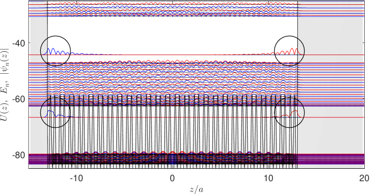
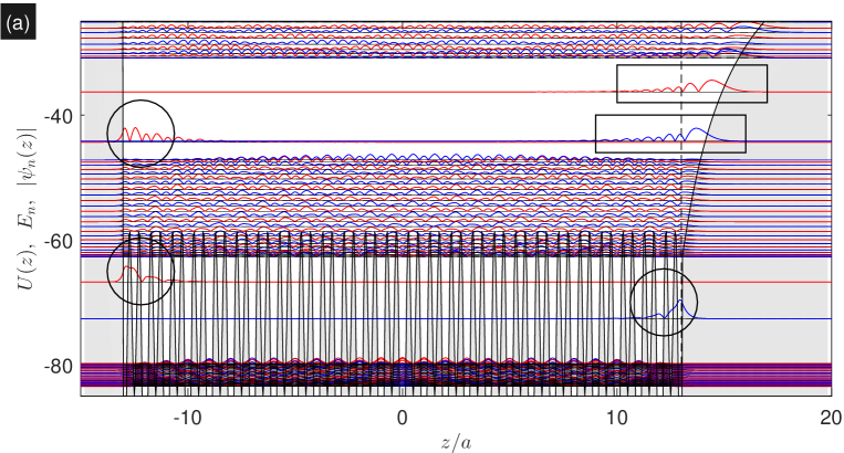
The results of the direct numerical solution of Eq. (S5) for the potential well with almost symmetrical edges ( and ) are presented in figure S7. One can see that the periodic potential induces well-known Tamm-Shockley surface states localized near the edges of the crystal with energies lying in the forbidden gaps of the bulk crystal. Figure S8 demonstrates the modification of both eigenfunctions and eigenvalues caused by a Coulomb-like potential near the right edge of the crystal (, panel a) and by a linearly increasing potential near the right edge of the crystal (, panel b).
These examples illustrate that all types of the considered surface states (namely, classical Tamm-Shockley states, image-potential states and states localized in a linearly increasing potential) are equivalent from the physical point of view. In addition, it is clear that the energies and the spatial structure of the wave functions of the localized states are very sensitive to the profile of the potential energy outside the potential well.
Mutual adjustment of the and dependences
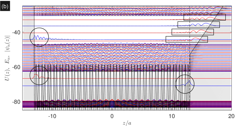
(a) Series of the dependences acquired for different tunneling currents: , 50, 100, 200, 300, 400, 500, 600, 800, 1000, 1200, 1400, 1600, 1800, 2200, 2600 and 3000 pA (from top to bottom). The color of the points is proportional to . All these curves are slightly shifted upward and downward (about 0.05 nm or less to compensate vertical thermal drift and creep effect of the piezoscanner) in such a way to get the correct dependence of on for the given bias (black dots in the panel b); this particular adjustment is performed for V, pA, nm (marked by ).
(b) Purple and black solid lines are the dependences of on , acquired during current-distance spectroscopy measurements for and +8 V, correspondingly. Purple and black dots represent the cross-sectional views for the data shown in the panel a along the dashed vertical lines for and +8 V, respectively. Almost perfect agreement between different kinds of measurements in panel b ensures the correctness of the visualization of the data in panel a.
The estimate of the FER energies based on the quasi-classical Wentzel-Kramers-Brillouin approximation
We consider the simplest quasiclassical 1D model and calculate the energy and spatial structure of the localized states in the linearly increasing potential. This model was partly presented in our recent paper (Aladyshkin, J. Phys.: Condens. Matt. 32, 435001 (2020)). This consideration is relevant for the particular cases of (i) a planar structure with a tunneling barrier of constant width and (ii) a very blunt STM tip above the sample surface. This model seems to be helpful for investigating the periodic nature of the quantized heights attributed to the th field-emission resonances.
The reflection coefficient for an electron from a flat surface of the sample apparently depends on the energy. The amplitude of the reflection coefficient can be close to unity if lies within the forbidden energy gap of the bulk crystal. Such almost ideal reflection ability in fact leads to the formation of the slow-decaying quasistationary electronic states localized above the sample in a linearly increasing potential. We therefore consider an effective triangular potential well (black solid line in Figure S11a)
| (S12) |
instead of a trapezoidal potential barrier
| (S16) |
Here is the Fermi energy of both electrodes (since the sample and the tip are in electrical contact,the Fermi levels of the electrodes are at the same energy); is the electric potential of the sample with respect to the tip, is the bias–shifted potential energy at the sample surface (at ); and are the work function for electrons of the sample and the tip, respectively; is the gradient of the potential energy which is proportional to the effective electric field above the surface; accounts for the Volta contact potential due to the difference in the work functions; and is the distance between the STM tip and the sample surface.
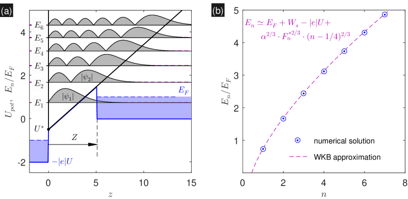
(b) Comparison of the eigenenergies obtained analytically [dashed line, Eq. (S21)] and numerically [, Eqs. (S24)–(S25)] for , and .
We start with the substitution of the quasi-classical momentum into the Bohr-Sommerfeld quantization rule
| (S17) |
where and are classical turning points, is the mass of free electron, is the integer index, and the numerical coefficient is close to 3/4 due to the presence of the impenetrable barrier at . We introduce the index for convenience. After integration, we obtain the discrete energy spectrum for the electrons localized in the triangular potential well
| (S18) |
Since the process of resonant tunnelling starts when the energy of the state localized in the area between the emitter (tip) and collector (sample) reaches the Fermi energy of the tip (), we come to the relationship
| (S19) |
The quasiclassical wave function of the electron localized in the triangular potential well near the right turning point can be written in the following form
| (S20) |
where is a constant. It is easy to see that the wave function at the left turning point is equal to zero provided that the argument of the cosine function is equal to
This equation is equivalent to Eq. (S18).
For convenient comparison of the analytic expression (S19) with the results of numerical simulations we introduce the following dimensionless parameters: the reduced energy , the reduced bias voltage , the reduced work function and as well as the reduced coordinate and the reduced barrier width , where is the natural energy scale and is the length scale. The expressions (S18) and (S19) can be written in the dimensionless form
| (S21) |
and
| (S22) |
By expressing via we get the dimensionless relationship for the th resonant value for the barrier width as a function of the bias voltage
| (S23) |
This implies that in this model the ratios for a given voltage have the universal form
Finally, the derived Schrodinger equation for determination of the real-valued eigenfunctions and eigenvalues for a particle trapped in the linearly increasing potential can be formulated in the dimensionless form as follows
| (S24) |
| (S25) |
The results of the numerical solution of Eqs. (S24) and (S25) for are presented in Figures S11a and S12a. The evolution of the quantized heights as a function of the voltage bias, described by Eq. (S23), is shown in Figure S12b.
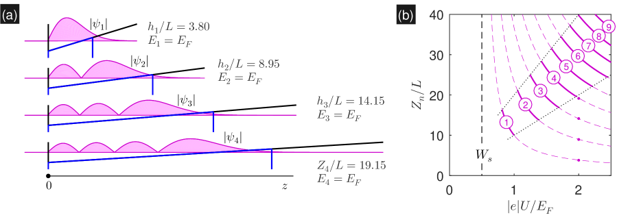
(b) The normalized quantized heights as a function of the dimensionless bias obtained analytically by means of Eq. (S23), where we take and . Two dotted lines depict schematically the range of experimentally accessible current values (compare this plot to figure 4a of the main paper).