Crystallization Dynamics of Amorphous Yttrium Iron Garnet Thin Films
Abstract
Yttrium iron garnet (YIG) is a prototypical material in spintronics due to its exceptional magnetic properties. To exploit these properties high quality thin films need to be manufactured. Deposition techniques like sputter deposition or pulsed laser deposition at ambient temperature produce amorphous films, which need a post annealing step to induce crystallization. However, not much is known about the exact dynamics of the formation of crystalline YIG out of the amorphous phase. Here, we conduct extensive time and temperature series to study the crystallization behavior of YIG on various substrates and extract the crystallization velocities as well as the activation energies needed to promote crystallization. We find that the type of crystallization as well as the crystallization velocity depend on the lattice mismatch to the substrate. We compare the crystallization parameters found in literature with our results and find an excellent agreement with our model. Our results allow us to determine the time needed for the formation of a fully crystalline film of arbitrary thickness for any temperature.
I Introduction
Yttrium iron garnet (\chY3Fe5O12, YIG) is an electrically insulating ferrimagnet, crystallizing in a cubic crystal system with Iad symmetry. Bertaut and Forrat (1956); Geller and Gilleo (1957) Its electric and magnetic properties include a long spin diffusion length, which makes YIG an ideal material for spin transport experiments with pure spin currents. Kajiwara et al. (2010); Althammer et al. (2013); Cornelissen et al. (2015) Additionally, YIG shows an exceptionally low Gilbert damping and a low coercive field, which allows investigations of magnon dynamics via e.g. ferromagnetic resonance experiments. Dillon (1957); Cherepanov et al. (1993); Wang et al. (2013); Sakimura et al. (2014); Anderson (1964)
These exceptional properties caused YIG to be intensively studied and made it the prototypical material in the field of spintronics, which almost exclusively relies on devices in thin film geometry. Several deposition techniques are known to produce high quality YIG thin films, including pulsed laser deposition (PLD), Heinrich et al. (2006); Krockenberger et al. (2008); Hauser et al. (2016, 2017); Heyroth et al. (2019); Gurjar et al. (2021); d’Allivy Kelly et al. (2013) liquid phase epitaxy (LPE) Shone (1985); Görnert et al. (1988); Čermák et al. (1990); Beaulieu et al. (2018) and radio-frequency (RF) magnetron sputtering. Park and Cho (2001); Jang and Kim (2001); Boudiar et al. (2004); Yamamoto et al. (2004); Kang et al. (2005); Block et al. (2014); Liu et al. (2014); Chang et al. (2014); Lustikova et al. (2014); Jungfleisch et al. (2015); Li et al. (2016); Cooper et al. (2017); Lian et al. (2017); Talalaevskij et al. (2017); Zhu et al. (2017); Ding et al. (2020a, b)
Some deposition techniques like magnetron sputtering give the opportunity to deposit both, amorphous and crystalline thin films, depending on the process temperatures during deposition. Jang and Kim (2001); Jang et al. (2004) Here, room temperature processes yield amorphous films. Park and Cho (2001); Jang and Kim (2001); Boudiar et al. (2004); Yamamoto et al. (2004); Kang et al. (2005); Block et al. (2014); Liu et al. (2014); Chang et al. (2014); Lustikova et al. (2014); Jungfleisch et al. (2015); Li et al. (2016); Cooper et al. (2017); Lian et al. (2017); Talalaevskij et al. (2017); Zhu et al. (2017); Ding et al. (2020a, b); Jang et al. (2004) For the deposition of YIG onto gadolinium gallium garnet (\chGd3Ga5O12, GGG) substrates, which feature a lattice constant very similar to the one of YIG, direct epitaxial growth was observed for process temperatures of . Jang and Kim (2001); Jang et al. (2004) On quartz a post annealing step is needed to enable the formation of polycrystalline YIG. Roumie et al. (2010)
The annealing process is usually performed under air Boudiar et al. (2004); Cooper et al. (2017) or reduced oxygen atmosphere Kang et al. (2005); Ding et al. (2020a) to counteract potential oxygen vacancies in the YIG lattice. For amorphous PLD films it has also been shown, that inert argon atmosphere has no deteriorating influence. Hauser et al. (2017)
The vast amount of publications highlight the interest in YIG. However, the influence of the post annealing step on the crystallization of the YIG thin film is only vaguely studied in the literature.
Here, we present an extended picture of the crystallization dynamics of YIG at different temperatures and annealing times, which allows us to define different crystallization windows depending on the substrate. Our results provide a general crystallographic description of the crystallization process for YIG thin films and summarize the crystallization parameters found in the literature.
II Methods
Ahead of the deposition, all substrates were cleaned for five minutes in aceton and isopropanol, and one minute in de-ionized water in an ultrasonic bath. YIG thin films were then deposited onto different substrate materials using RF sputtering from a YIG sinter target at argon pressure and power, at a rate of . The nominal thickness upon deposition was . The post-annealing steps were carried out in a tube zone furnace under air.
As substrates yttrium aluminum garnet (\chY3Al5O12, YAG, CrysTec) and gadolinium gallium garnet (\chGd3Ga5O12, GGG, SurfaceNet) with a <111> crystal orientation along the surface normal were used. Additionally, silicon wafers cut along the <> crystal direction with a thick thermal oxide layer (\chSi/\chSiO_x, MicroChemicals) were used. Since GGG and YAG crystallize in the same space group Iad as YIG and their lattice parameters are Gates-Rector and Blanton (2019a) and , Gates-Rector and Blanton (2019b) respectively, they are considered lattice matched in regards to the for YIG. Gates-Rector and Blanton (2019c) The lattice mismatch can be calculated with Eq. (1)
| (1) |
and translates to for GGG and for YAG. Gross and Marx (2014) Due to the amorphous \chSiO_x layer the \chSi/\chSiO_x substrates do not provide any preferential direction for crystallization. But even considering the underlying Si layer, we do not expect it to influence the crystallization direction in any way, as it features a fundamentally different space group (Fdm) and lattice constant. Gates-Rector and Blanton (2019d) Therefore, \chSi/\chSiO_x is considered non lattice matched and fulfills the function as an arbitrary substrate.
For the structural characterization X-ray diffraction measurements (XRD) were performed using a Rigaku Smart Lab Diffractometer with Cu radiation. Scanning electron microscopy as well as electron backscatter diffraction (EBSD) measurements were conducted using a Zeiss Gemini Scanning Electron Microscope (SEM). The magnetic properties were characterized by determining the magnetooptical polarization rotation in a Kerr-Microscope from Evico Magnetics.
III Results and Discussion
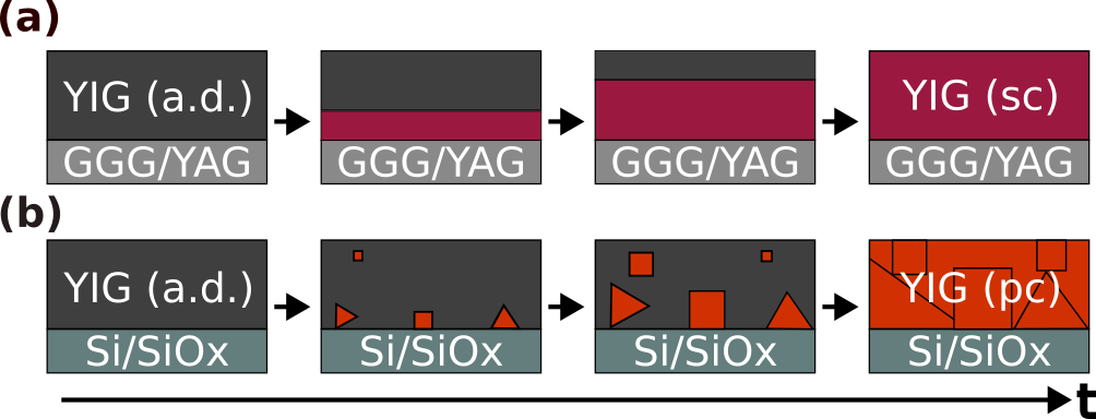
The crystallization mechanism of a thin film crucially depends on the substrate: for substrates where the lattices of film and substrate are sufficiently similar, the thin film layer crystallizes epitaxially, whereas for a substrate where the two lattices do not match, nucleation is needed.
Figure 1 shows the different growth mechanisms and the resulting YIG micro structure depending on the chosen substrate. As depicted in Figure 1(a), a lattice matched substrate acts as a seed on which the film can grow epitaxially. Therefore, a single crystalline front is expected to move from the substrate on towards the upper boundary of the film, Csepregi et al. (1975, 1976) which is commonly referred to as solid phase epitaxy (SPE) in the literature. For a substrate with a sufficiently large lattice mismatch or no crystalline order, no such surface is given, see Fig. 1(b). Here, a nucleus needs to be formed first from which further crystallization takes place. The formation of the initial seeds by nucleation is expected to take place randomly. The polycrystalline seeds grow until reaching another grain or one of the sample’s boundaries. For any of these processes, SPE or nucleation, to take place, the system needs to be at a temperature characteristic for this specific thin film/substrate system. Chen et al. (2017)
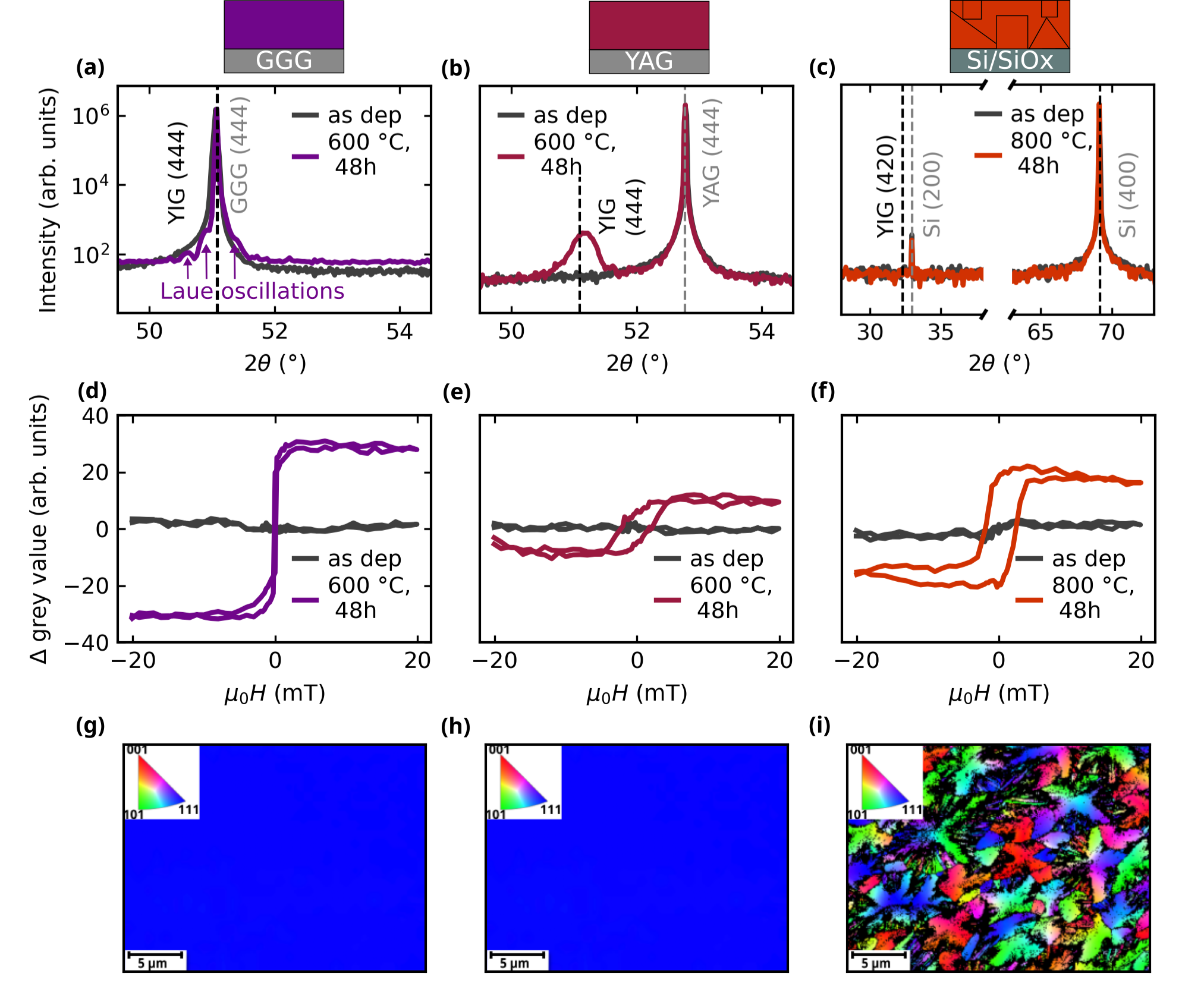
To distinguish between amorphous, partly and fully crystalline films we apply several characterization methods, probing the structural and magnetic properties of the YIG thin films. The typical fingerprints of amorphous versus crystalline YIG on different substrates as determined by X-ray diffraction (XRD), magneto-optical Kerr microscopy (MOKE) and electron back scatter diffraction (EBSD) are depicted in Figure 2. From top to bottom we gain an increased spacial resolution, probing increasingly smaller areas of the sample.
With XRD, the structural properties of YIG on YAG and GGG can be evaluated. For the amorphous films, the XRD measurements in Fig. 2 (a-c) show a signal stemming only from the substrate (cp. gray dashed lines). Upon annealing, YIG is visible in the form of Laue-oscillations on GGG (purple) and as a peak on YAG (red). In stark contrast to that no signal, which could be attributed to YIG, can be found on \chSiO_x, even when annealing at for . The sharp peak in Fig. 2(c) at can be attributed to a detour excitation of the substrate, as it is visible in the as deposited state and fits the forbidden Si (200) peak. Renninger (1937) In the literature, YIG on \chSiO_x has been reported to be polycrystalline at lower annealing temperatures than in the exemplary data shown in Fig. 2(c). Boudiar et al. (2004); Kang et al. (2005); Roumie et al. (2010) These films show peaks in the XRD, however they were at least one order of magnitude thicker. We therefore do not expect the YIG layer on \chSi/\chSiO_x to be amorphous, which will be confirmed in the following.
By probing the magnetic properties of the thin films with MOKE (cp. Fig. 2(d-f)), a clear distinction between amorphous and crystalline YIG can be made. While the film shows a linear MOKE signal in the as-deposited state, it changes to a hysteresis for all three samples upon annealing. In general, the sharpest hysteresis is visible for YIG on GGG, which becomes broader for an increasing structural misfit. Naïvely polycrystalline samples are expected to consist of multiple domains pointing towards different directions, which lead to an increase of the coercive field. This is consistent with our results and also with the magnetic properties found in literature. Kang et al. (2005); Zheng et al. (2014); Li et al. (2016); Hauser et al. (2016) These coercive fields are below for YIG on GGGLi et al. (2016); Hauser et al. (2016) and between 2.2- for YIG on \chSi/\chSiO_x.Kang et al. (2005); Zheng et al. (2014) The MOKE measurements therefore indicate the spontaneous formation of a phase with magnetic ordering on all three substrates.
While MOKE correlates the magnetic properties with amorphous and crystalline films, it lacks the ability to quantify the amount of crystalline YIG. The hysteretic response for the annealed YIG on \chSiO_x strongly supports the formation of crystalline YIG, however, we cannot correlate this to a percentage of crystalline material. Therefore, a structural characterization with higher spacial resolution than XRD is needed.
To that end electron back scatter diffraction (EBSD) measurements were performed. With this technique Kikuchi patterns, which are correlated to the crystal structure, are detected and later evaluated. The results are shown for crystalline samples only, as the amorphous film showed no Kikuchi patterns. This confirms, that the detected patterns stem from the YIG thin film itself and not from the crystallographically similar substrates of YAG or GGG. This is consistent with the EBSD signal depth given in the literature of 10 to . Dingley (2004) The extracted crystal orientations along the surface normal can be seen in Fig. 2 (g-i). On YAG and GGG a single color corresponding to the <> direction is visible in the mapping, which is consistent with the XRD data and corroborates the epitaxial growth from the substrate in the <> direction. On \chSiO_x, however, various crystal directions are present, confirming the polycrystalline nature of the YIG. The crystallographic data from our EBSD measurements show random nucleation. The cross shape of the individual crystalline areas point towards an anisotropic crystallization with a preferential direction along <> or higher indexed directions like <>, which is consistent with earlier studies on YIG and other rare earth garnets Nielsen and Dearborn (1958); Tolksdorf and Bartels (1981); Bennema et al. (1983); Park and Cho (2001) as well as PLD grown bismuth iron garnet. Heinrich et al. (2006).
Using EBSD allows for a quantification of the amount of crystalline material for a YIG thin film on \chSiO_x or any arbitrary substrate. Combining the magnetic and structural data from MOKE and EBSD, respectively, allows for an unambiguous identification of the formation of polycrystalline YIG on \chSiO_x, which was not possible by XRD.
We presume that the absence of any XRD peaks results from the small volume of the individual crystallites of YIG on \chSiO_x. We approximate the volume of a single polycrystalline grain, i.e. one cross from the EBSD data (cp. Fig. 2(i)) to be , stemming from an area of about and a film thickness of . This is also the size of individually contributing grains to the diffraction within the XRD. Assuming a single crystalline thin film, where the whole irradiated area contributes additively, the contributing area amounts to , which is six orders of magnitude larger than that of an individual grain. Therefore, the contributions of the individual grains of the YIG layer on \chSiO_x to the XRD intensity are too small to result in a finite peak for a thick film.
These results provide the basis for the investigation of the crystallization behavior and reveal how different techniques enable us to distinguish between amorphous, partly and fully crystalline films. We utilize the structural information to analyze the crystallization dynamics on the different substrates.
The percentage of crystalline YIG was quantified differently for the three different substrates. For YIG on YAG the amount of crystalline YIG correlates to the intensity of the Bragg peak. A certain film thickness corresponds to a maximum area under the peak, to which the intensity is normalized. For YIG on GGG, the percentage of crystalline YIG is extracted from the Laue oscillations (cp. Fig 2(a)). The frequency of the oscillation corresponds to the number of interfering lattice planes, enabling the calculation of the thickness of the crystalline layer. Using X-ray reflectivity, the absolute film thickness was measured for each film. Comparing the thickness of the crystalline layer with the film thickness then enables to monitor the growth of YIG on GGG. For the non lattice matched substrates, EBSD mappings were taken to extract the amount of crystalline YIG. For each of the YIG thin films, a percentage of crystalline YIG at a given time and temperature is extracted, which allows an evaluation of the crystallization process for this specific temperature.
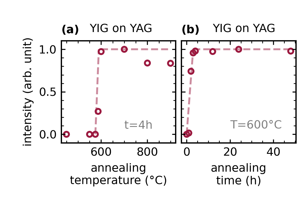
First, we find the onset temperature for the crystallization of YIG on each substrate. As crystallization is thermally activated, it depends exponentially on the annealing temperature, Avrami (1939) which leads to a very narrow temperature window of incomplete crystallization. To extract this window, multiple samples were annealed for four hours at different temperatures. Figure 3(a) exemplarily shows the results for YIG on YAG, where after a steep increase in intensity up to a maximum at can be seen. This intensity value stays the same for , which suggests, that the YIG film is fully crystallized and no further increase in intensity is expected. A crystalline YIG film on YAG can therefore be obtained at a temperature range around . For YIG on GGG this window is found to be slightly below , whereas on \chSiO_x, we found the first indication of crystallization at .
For our samples, the heating up and cooling down is included in the annealing time. An in-situ study on a representative sample with yielded data in a good agreement to the crystallization behavior in the one zone furnace. Please note that the use of different equipment led to a small variation in absolute temperature (see supplementary information).
The lower intensities at and above (cp. Fig. 3(a)) hint towards the occurrence of competing growth processes. We attribute the reduction in intensity at annealing temperatures above to additional growth of polycrystalline grains enabled by the elevated temperatures, which competes with the epitaxial growth and by that reduces the crystal quality of the thin film. Analyzing the rocking curves of these samples (see supplementary information) confirms an increased full width at half maximum value towards higher temperatures. This can be correlated with a lower crystal quality, which supports an additional polycrystalline growth.
To study the crystallization dynamics, the time evolution of the intensity for a given temperature was evaluated, again representatively shown for YIG on YAG in Fig. 3(b). Here, one sample was subjected to the same temperature for multiple repeats until the extracted intensity of the YIG peak and therewith the crystalline area did saturate. This saturation represents a fully crystallized thin film, where no further changes are expected.
To describe the crystallization at an arbitrary temperature, we find a general crystallographic description for each of the substrates. A phase transition in a solid like crystallization can generally be described by the Avrami equation: Avrami (1939); William and Mehl (1939); Avrami (1940, 1941)
| (2) |
where, is the crystallinity normalized to one, with respect to a complete crystallization, the rate constant and the annealing time. The exponent is often referred to as the Avrami exponent and describes how the crystallization takes place.Avrami (1940) It can take values between 1 and 4, where one contribution stems from the nucleation and takes values of 0 for controlled and 1 for random nucleation, while the other contributions originate from the type of crystallization in the three spacial directions.
For the rate constant k we use an exponential Arrhenius dependency:Callister (2007); Csepregi et al. (1975)
| (3) |
where both the pre-factor and the activation energy are unique for each combination of film and substrate material.
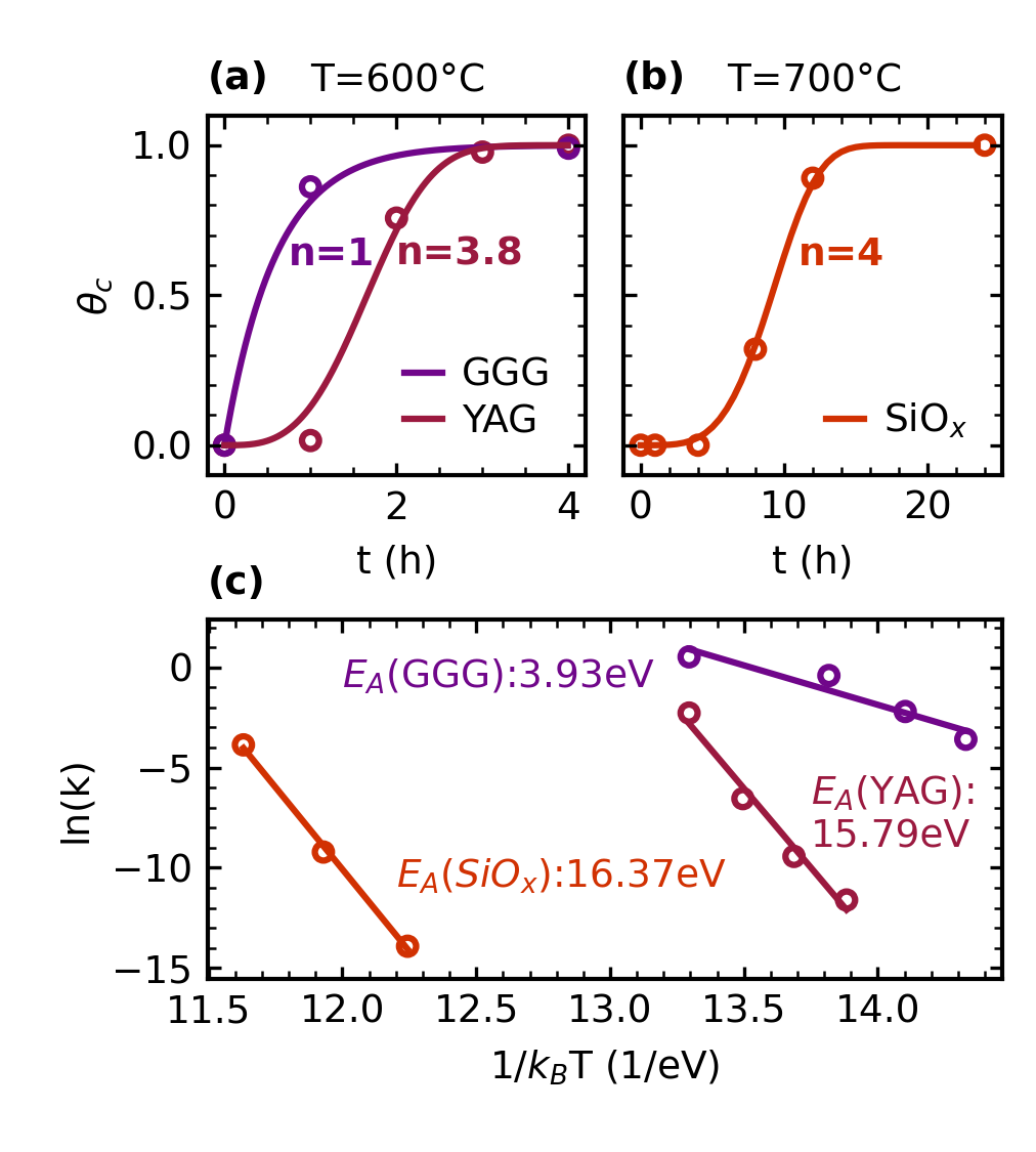
The Avrami equation (cp. Eq.(2)) lets us describe the crystallization on all three substrates. To that end we fit the normalized crystallinity values of YIG with the Avrami equation (cp. Eq.(2)), where we fix the Avrami exponent n between and (cp. Fig. 4(a)+(b)). The rate constants then describe the growth velocities on the respective substrate in . The crystallization behavior of YIG on GGG and YAG at an annealing temperature of is shown in Fig. 4(a).
On GGG at (cp. Fig. 4(a)), YIG immediately starts to crystallize with a rate constant of and an Avrami exponent of 1. This means, that the crystallization takes place without nucleation and in one spacial direction, which is consistent with the monotonously moving crystallization front expected for SPE. The rate constant translates to a starting velocity of for the films. Towards longer annealing times, the curve flattens, meaning that the crystalline material reaches the sample’s surface.
The crystallization of YIG on YAG shows an initial time delay, despite the comparably small lattice mismatch of (cp. Fig. 4(a)). The fitting of the data at leads to a rate constant of with . This means, that the crystallization does not follow a typical SPE behavior and nucleation processes in the thin film cannot be excluded. However, also for the crystallization on YAG, single crystalline YIG is obtained (cp. Fig. 2(b)+(h)). This deviation from YIG on GGG is most likely due to the larger lattice mismatch which causes an energetically costly strain in the film. Wang et al. (2014) The crystallization velocity along the surface normal direction is obtained by the -th root out of the rate constant and translates to .
The crystallization of YIG on \chSiO_x is fundamentally different (cp. Fig. 4(b)). Here, polycrystalline grains could be found at temperatures of and above. The time evolution of the crystallinity is depicted in Figure 4(b), where fitting the data by the Avrami equation (Eq. (2)) yields with and a rate constant of . This confirms our initial hypothesis of nucleation and subsequent three dimensional growth. Higher temperatures compared to the garnet substrates are needed to provide enough energy for nucleation, which causes the crystallization process to be visible at and above.
An approximation of the crystallization velocity can be extracted from the EBSD data. Here, we assume that the crystallization starts in the middle of a cross shape structure (cp. Fig. 2(i)) and stops when reaching a boundary given by neighboring crystallites. The distance covered depends on the number of nuclei formed and is highly dependent on the direction. To ensure comparability with the two lattice matched substrates, we consider grains growing in plane along the <> direction. At , the YIG crystallites on \chSiO_x measured up to in length after at least of annealing. This translates into a propagation velocity of at on an arbitrary substrate along the <> direction.
To compare the three crystallization velocities, the temperature dependence of the rate constants needs to be taken into consideration. Using the Arrhenius equation (Eq. (3)) we are able to extrapolate the crystallization rate at any temperature. To that end, the logarithm of each rate constant is plotted over the inverse temperature. The linear dependency of Eq. (3) in the logarithmic plot allows us to extract the activation energy and the pre-factor for YIG on each substrate. The resulting values are plotted in Tab. 1. While at first glance the crystallization velocity for YIG on \chSiO_x seems faster, the different annealing temperatures of for the garnet substrates and for \chSiO_x need to be taken into account (cp. Fig.4). Extrapolating the growth velocity for YIG on GGG at reveals that here YIG would crystallize approximately 30 times faster than on \chSiO_x.
Our activation energy of for YIG on GGG is in good agreement with the literature. For the formation of bulk YIG from oxide powders, a value of was reported. Wan Ali et al. (2016) Further, for the crystallization of bulk polycrystalline YAG, which is expected to behave similarly as it has the same crystal structure, an activation energy of was found.Johnson and Kriven (2001) The lower value of for YIG on GGG highlights the reduced energy needed, due to the growth from the lattice matched GGG.
The activation energies for YIG on YAG as well as on \chSiO_x are much higher than the value on GGG. As the general crystallization windows and times needed for a fully crystalline film stay the same, we ascribe this behavior to a kinetic blocking, originating from the lattice mismatch and the nucleation. Understanding the exact mechanism however, would need further study.
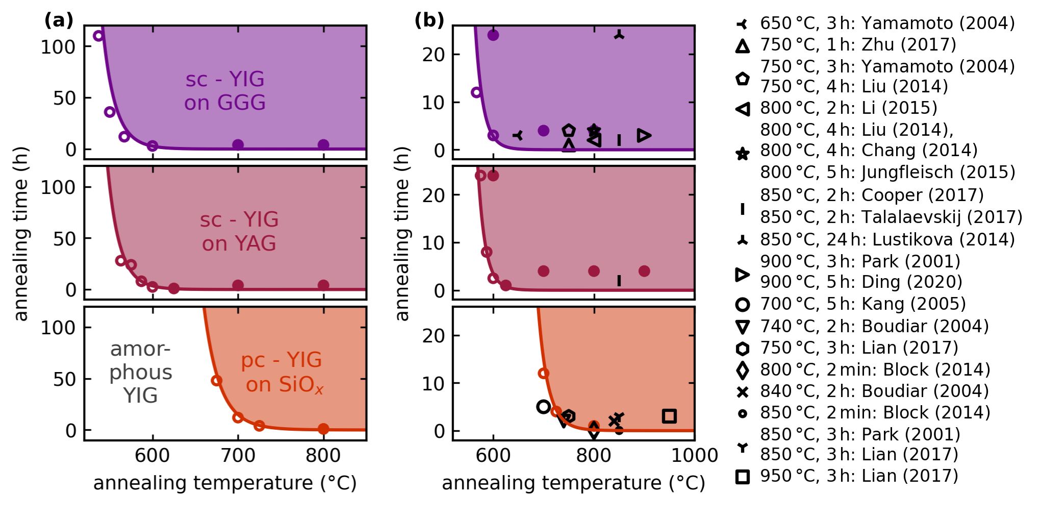
These results allow to establish a diagram to underline which annealing parameters will lead to a fully crystalline YIG thin film on the three substrates (cp. Fig. 5(a)). For a mathematical description, we combine the Avrami equation Eq. (2) with the Arrhenius equation Eq. (3) to be able to express the crystallinity in terms of annealing time and temperature.
| (4) |
We use a crystallinity of 0.999 to avoid the divergence of the logarithm and the respective , and found in Tab. 1.
| (eV) | () | n | |
| YIG on GGG | 0.86 | 1 | |
| YIG on YAG | 1.59 | 3.8 | |
| YIG on \chSiO_x | 0.85 | 4 | |
Figure 5(a) outlines the temperature and time combination where crystalline YIG (shaded areas) can be obtained. Regions where the YIG thin film remains amorphous are left in white. The boundary between non crystalline and crystalline for each substrate is given by Eq. (4). Each of the circles seen in Fig. 5(a) represents one fully crystalline sample obtained as described for Fig. 3(b). The filled circles represent fully crystalline samples, where no time dependence of the crystallinity was measured. As already anticipated, YIG exhibits different crystallization behavior depending on the substrate. Note, that polycrystalline growth on \chSiO_x or any arbitrary substrate needs notably higher temperatures than epitaxial growth, where an annealing at for would be necessary to result in a fully crystalline film.
The different temperatures and times necessary to induce crystallization stem from the different types of substrates. For YIG on GGG and YAG the seed for the crystallization is given by the lattice of the substrate. Therefore, we ascribe the discrepancy between YAG and GGG to the different lattice mismatch compared to YIG. In the YIG thin films on YAG a higher strain is expected to exist in the film, which leads to the formation of energetically costly dislocations. This in turn results in the slightly higher temperature needed for YIG to crystallize on YAG. On \chSiO_x, however, a significantly higher temperature than for the lattice matched substrates is needed for crystalline YIG to form. Here, as no initial seed is given by the substrate, nucleation is required, which is a thermally activated process that needs additional energy, i.e. higher temperatures. This random formation of seeds leads to a polycrystalline YIG thin film on \chSiO_x
A comparison with the literature shows, that parameters which have been previously reported to result in a fully crystalline YIG layer, fit into our extracted area, (cp. Fig. 5(b)).Park and Cho (2001); Jang and Kim (2001); Boudiar et al. (2004); Yamamoto et al. (2004); Kang et al. (2005); Block et al. (2014); Liu et al. (2014); Chang et al. (2014); Lustikova et al. (2014); Jungfleisch et al. (2015); Li et al. (2016); Cooper et al. (2017); Lian et al. (2017); Talalaevskij et al. (2017); Zhu et al. (2017); Ding et al. (2020a, b) Additionally to the sputtered films, also amorphous films obtained from PLD with subsequent annealing fit in the observed regions. Heinrich et al. (2006); Krockenberger et al. (2008); Hauser et al. (2016, 2017); Heyroth et al. (2019); Gurjar et al. (2021) The extracted diagram in Fig. 5 therefore acts as a general description for the crystallization of YIG thin films out of the amorphous phase.
IV Conclusion
An extensive time and temperature series was used to analyze the crystallization kinetics of sputtered amorphous YIG thin films on different substrates. We find the formation of single crystalline YIG thin films on garnet substrates where the growth on gadolinium gallium garnet can be coherently described in a solid-phase epitaxy picture, whereas a more complicated growth scheme is found on yttrium aluminum garnet. On \chSiO_x a polycrystalline YIG thin film develops, with slower crystallization dynamics than for the garnet substrates.
A fully crystalline YIG film on GGG was found for temperatures as low as and annealing times of . On silicon oxide (representing any type of amorphous or non lattice matched substrate), the nucleation of the YIG crystals is not expected for reasonable time scales below . The results summarized in Tab. 1 allow for the determination of the crystallization velocity of YIG on those substrates for any temperature.
Thus, we provide a complete description of the crystallization process from the amorphous phase for YIG on GGG, YAG and arbitrary substrates such as \chSiO_x, which allows us to define the range in which crystalline YIG thin films can be obtained.
V Acknowledgments
This work was funded by the Deutsche Forschungsgemeinschaft (DFG, German Research Foundation) – Project-ID 446571927. We cordially thank F. Michaud and J. Ben Youssef from the Université de Bretagne Occidentale in Brest (France) for fruitful discussions and for letting us use their in-situ X-ray diffractometer. We also gratefully acknowledge technical support and advice by the nano.lab facility of the University Konstanz.
VI References
References
- Bertaut and Forrat (1956) F. Bertaut and F. Forrat, Comptes Rendus Hebdomadaires Des Seances De L Academie Des Sciences 242, 382 (1956).
- Geller and Gilleo (1957) S. Geller and M. Gilleo, Journal of Physics and Chemistry of Solids 3, 30 (1957).
- Kajiwara et al. (2010) Y. Kajiwara, K. Harii, S. Takahashi, J. Ohe, K. Uchida, M. Mizuguchi, H. Umezawa, H. Kawai, K. Ando, K. Takanashi, S. Maekawa, and E. Saitoh, Nature 464, 262 (2010).
- Althammer et al. (2013) M. Althammer, S. Meyer, H. Nakayama, M. Schreier, S. Altmannshofer, M. Weiler, H. Huebl, S. Geprägs, M. Opel, R. Gross, D. Meier, C. Klewe, T. Kuschel, J.-M. Schmalhorst, G. Reiss, L. Shen, A. Gupta, Y.-T. Chen, G. E. W. Bauer, E. Saitoh, and S. T. B. Goennenwein, Phys. Rev. B 87, 224401 (2013).
- Cornelissen et al. (2015) L. Cornelissen, J. Liu, R. Duine, J. B. Youssef, and B. Van Wees, Nature Physics 11, 1022 (2015).
- Dillon (1957) J. F. Dillon, Phys. Rev. 105, 759 (1957).
- Cherepanov et al. (1993) V. Cherepanov, I. Kolokolov, and V. L’vov, Physics Reports 229, 81 (1993).
- Wang et al. (2013) H. L. Wang, C. H. Du, Y. Pu, R. Adur, P. C. Hammel, and F. Y. Yang, Phys. Rev. B 88, 100406(R) (2013).
- Sakimura et al. (2014) H. Sakimura, T. Tashiro, and K. Ando, Nature Communications 5, 5730 (2014).
- Anderson (1964) E. E. Anderson, Phys. Rev. 134, A1581 (1964).
- Heinrich et al. (2006) A. Heinrich, S. Leitenmeier, T. Körner, R. Lux, M. Herbort, and B. Stritzker, Journal of the Magnetics Society of Japan 30, 584 (2006).
- Krockenberger et al. (2008) Y. Krockenberger, H. Matsui, T. Hasegawa, M. Kawasaki, and Y. Tokura, Applied Physics Letters 93, 092505 (2008).
- Hauser et al. (2016) C. Hauser, T. Richter, N. Homonnay, C. Eisenschmidt, M. Qaid, H. Deniz, D. Hesse, M. Sawicki, S. Ebbinghaus, and G. Schmidt, Scientific Reports 6, 20827 (2016).
- Hauser et al. (2017) C. Hauser, C. Eisenschmidt, T. Richter, A. Müller, H. Deniz, and G. Schmidt, Journal of Applied Physics 122, 083908 (2017).
- Heyroth et al. (2019) F. Heyroth, C. Hauser, P. Trempler, P. Geyer, F. Syrowatka, R. Dreyer, S. G. Ebbinghaus, G. Woltersdorf, and G. Schmidt, Phys. Rev. Applied 12, 054031 (2019).
- Gurjar et al. (2021) G. Gurjar, V. Sharma, S. Patnaik, and B. K. Kuanr, Mater. Res. Express 8, 066401 (2021).
- d’Allivy Kelly et al. (2013) O. d’Allivy Kelly, A. Anane, R. Bernard, J. Ben Youssef, C. Hahn, A. H. Molpeceres, C. Carrétéro, E. Jacquet, C. Deranlot, P. Bortolotti, R. Lebourgeois, J.-C. Mage, G. De Loubens, O. Klein, V. Cros, and A. Fert, Appl. Phys. Lett. 103, 082408 (2013).
- Shone (1985) M. Shone, Circuits, Systems and Signal Processing 4, 89 (1985).
- Görnert et al. (1988) P. Görnert, R. Hergt, E. Sinn, M. Wendt, B. Keszei, and J. Vandlik, Journal of Crystal Growth 87, 331 (1988).
- Čermák et al. (1990) J. Čermák, A. Abrahám, T. Fabián, P. Kaboš, and P. Hyben, Journal of Magnetism and Magnetic Materials 83, 427 (1990).
- Beaulieu et al. (2018) N. Beaulieu, N. Kervarec, N. Thiery, O. Klein, V. Naletov, H. Hurdequint, G. De Loubens, J. B. Youssef, and N. Vukadinovic, IEEE Magn. Lett. 9, 1 (2018).
- Park and Cho (2001) M.-B. Park and N.-H. Cho, Journal of Magnetism and Magnetic Materials 231, 253 (2001).
- Jang and Kim (2001) P. W. Jang and J. Y. Kim, IEEE Transactions on Magnetics 37, 2438 (2001).
- Boudiar et al. (2004) T. Boudiar, B. Payet-Gervy, M.-F. Blanc-Mignon, J.-J. Rousseau, M. Le Berre, and H. Joisten, Journal of Magnetism and Magnetic Materials 284, 77 (2004).
- Yamamoto et al. (2004) S. Yamamoto, H. Kuniki, H. Kurisu, M. Matsuura, and P. Jang, phys. stat. sol. (a) 201, 1810 (2004).
- Kang et al. (2005) Y.-M. Kang, S.-H. Wee, S.-I. Baik, S.-G. Min, S.-C. Yu, S.-H. Moon, Y.-W. Kim, and S.-I. Yoo, Journal of Applied Physics 97, 10A319 (2005).
- Block et al. (2014) A. D. Block, P. Dulal, B. J. H. Stadler, and N. C. A. Seaton, IEEE Photonics J. 6, 1 (2014).
- Liu et al. (2014) T. Liu, H. Chang, V. Vlaminck, Y. Sun, M. Kabatek, A. Hoffmann, L. Deng, and M. Wu, Journal of Applied Physics 115, 17A501 (2014).
- Chang et al. (2014) H. Chang, P. Li, W. Zhang, T. Liu, A. Hoffmann, L. Deng, and M. Wu, IEEE Magn. Lett. 5, 1 (2014).
- Lustikova et al. (2014) J. Lustikova, Y. Shiomi, Z. Qiu, T. Kikkawa, R. Iguchi, K. Uchida, and E. Saitoh, Journal of Applied Physics 116, 153902 (2014).
- Jungfleisch et al. (2015) M. B. Jungfleisch, W. Zhang, W. Jiang, H. Chang, J. Sklenar, S. M. Wu, J. E. Pearson, A. Bhattacharya, J. B. Ketterson, M. Wu, and A. Hoffmann, Journal of Applied Physics 117, 17D128 (2015).
- Li et al. (2016) S. Li, W. Zhang, J. Ding, J. E. Pearson, V. Novosad, and A. Hoffmann, Nanoscale 8, 388 (2016).
- Cooper et al. (2017) J. F. K. Cooper, C. J. Kinane, S. Langridge, M. Ali, B. J. Hickey, T. Niizeki, K. Uchida, E. Saitoh, H. Ambaye, and A. Glavic, Phys. Rev. B 96, 104404 (2017).
- Lian et al. (2017) J. Lian, Y. Chen, Z. Liu, M. Zhu, G. Wang, W. Zhang, and X. Dong, Ceramics International 43, 7477 (2017).
- Talalaevskij et al. (2017) A. Talalaevskij, M. Decker, J. Stigloher, A. Mitra, H. S. Körner, O. Cespedes, C. H. Back, and B. J. Hickey, Phys. Rev. B 95, 064409 (2017).
- Zhu et al. (2017) N. Zhu, H. Chang, A. Franson, T. Liu, X. Zhang, E. Johnston-Halperin, M. Wu, and H. X. Tang, Appl. Phys. Lett. 110, 252401 (2017).
- Ding et al. (2020a) J. Ding, C. Liu, Y. Zhang, U. Erugu, Z. Quan, R. Yu, E. McCollum, S. Mo, S. Yang, H. Ding, X. Xu, J. Tang, X. Yang, and M. Wu, Phys. Rev. Appl. 14, 014017 (2020a).
- Ding et al. (2020b) J. Ding, T. Liu, H. Chang, and M. Wu, IEEE Magn. Lett. 11, 1 (2020b).
- Jang et al. (2004) P. Jang, S. Yamamoto, and H. Kuniki, physica status solidi (a) 201, 1851 (2004).
- Roumie et al. (2010) M. Roumie, B. A. Samad, M. Tabbal, M. Abi-Akl, M.-F. Blanc-Mignon, and B. Nsouli, Materials Chemistry and Physics 124, 188 (2010).
- Gates-Rector and Blanton (2019a) S. Gates-Rector and T. Blanton, Powder Diffraction (PDF: 00-013-0493) 34, 352 (2019a).
- Gates-Rector and Blanton (2019b) S. Gates-Rector and T. Blanton, Powder Diffraction (PDF: 00-033-0040) 34, 352 (2019b).
- Gates-Rector and Blanton (2019c) S. Gates-Rector and T. Blanton, Powder Diffraction (PDF: 00-043-0507) 34, 352 (2019c).
- Gross and Marx (2014) R. Gross and A. Marx, Festkörperphysik, 2nd ed. (De Gruyter, Berlin ; Boston, 2014).
- Gates-Rector and Blanton (2019d) S. Gates-Rector and T. Blanton, Powder Diffraction (PDF: 00-005-0565) 34, 352 (2019d).
- Csepregi et al. (1975) L. Csepregi, J. Mayer, and T. Sigmon, Physics Letters A 54, 157 (1975).
- Csepregi et al. (1976) L. Csepregi, J. W. Mayer, and T. W. Sigmon, Appl. Phys. Lett. 29, 92 (1976).
- Chen et al. (2017) Y. Chen, M. H. Yusuf, Y. Guan, R. Jacobson, M. G. Lagally, S. E. Babcock, T. F. Kuech, and P. G. Evans, ACS Applied Materials & Interfaces 9, 41034 (2017).
- Renninger (1937) M. Renninger, Zeitschrift für Physik 106, 141 (1937).
- Zheng et al. (2014) H. Zheng, J. Zhou, J. Deng, P. Zheng, L. Zheng, M. Han, Y. Yang, L. Deng, and H. Qin, Materials Letters 123, 181 (2014).
- Dingley (2004) D. Dingley, Journal of Microscopy 213, 214 (2004).
- Nielsen and Dearborn (1958) J. W. Nielsen and E. F. Dearborn, Journal of Physics and Chemistry of Solids 5, 202 (1958).
- Tolksdorf and Bartels (1981) W. Tolksdorf and I. Bartels, Journal of Crystal Growth 54, 417 (1981).
- Bennema et al. (1983) P. Bennema, E. A. Giess, and J. E. Weidenborner, Journal of Crystal Growth 62, 41 (1983).
- Avrami (1939) M. Avrami, The Journal of Chemical Physics 7, 1103 (1939).
- William and Mehl (1939) J. William and R. Mehl, Trans. Metall. Soc. AIME 135, 416 (1939).
- Avrami (1940) M. Avrami, The Journal of Chemical Physics 8, 212 (1940).
- Avrami (1941) M. Avrami, The Journal of Chemical Physics 9, 177 (1941).
- Callister (2007) W. D. Callister, Materials science and engineering: an introduction, 7th ed. (John Wiley & Sons, New York, 2007) oCLC: ocm61463872.
- Wang et al. (2014) H. Wang, C. Du, P. C. Hammel, and F. Yang, Phys. Rev. B 89, 134404 (2014).
- Wan Ali et al. (2016) W. F. F. Wan Ali, M. Othman, M. F. Ain, N. S. Abdullah, and Z. A. Ahmad, J. Am. Ceram. Soc. 99, 315 (2016).
- Johnson and Kriven (2001) B. R. Johnson and W. M. Kriven, J. Mater. Res. 16, 1795 (2001).