Realization of the quantum ampere using the quantum anomalous Hall and Josephson effects
Linsey K. Rodenbach1,2,3†, Ngoc Thanh Mai Tran3,4†, Jason M. Underwood3†, Alireza R. Panna3, Molly P. Andersen2,5, Zachary S. Barcikowski3,4, Shamith U. Payagala3, Peng Zhang6, Lixuan Tai6, Kang L. Wang6, Randolph E. Elmquist3, Dean G. Jarrett3, David B. Newell3, Albert F. Rigosi3 and David Goldhaber-Gordon1,2a
1Department of Physics, Stanford University, Stanford, California 94305, USA
2Stanford Institute for Materials and Energy Sciences, SLAC National Accelerator Laboratory, 2575 Sand Hill Road, Menlo Park, California 94025, USA
3Physical Measurement Laboratory, National Institute of Standards and Technology (NIST), Gaithersburg, Maryland 20899, USA
4Joint Quantum Institute, University of Maryland, College Park, Maryland 20742, USA
5Department of Materials Science and Engineering, Stanford University, Stanford, California 94305, USA
6Department of Electrical and Computer Engineering, Department of Physics and Astronomy, University of California, Los Angeles, California 90095, USA
†These authors contributed equally to this work.
aTo whom correspondence should be addressed; E-mail: goldhaber-gordon@stanford.edu
By directly coupling a quantum anomalous Hall resistor to a programmable Josephson voltage standard, we have implemented a quantum current sensor (QCS) that operates within a single cryostat in zero magnetic field. Using this QCS we determine values of current within the range 9.33 nA – 252 nA, providing a realization of the ampere based on fundamental constants and quantum phenomena. The relative Type A uncertainty is lowest, 2.3010-6 A/A, at the highest current studied, 252 nA. The total root-sum-square combined relative uncertainty ranges from 3.91 10-6 A/A at 252 nA to 41.2 10-6 A/A at 9.33 nA. No DC current standard is available in the nanoampere range with relative uncertainty comparable to this, so we assess our QCS accuracy by comparison to a traditional Ohm’s law measurement of the same current source. We find closest agreement (1.46 4.28)10-6 A/A for currents near 83.9 nA, for which the highest number of measurements were made.
I. Introduction
In 2019, the International System of Units (SI) was redefined to link the seven base units to physical constants in nature [1, 2, 3]. Under the new SI, units are defined solely through their relation to fixed-value fundamental constants. This redefinition removed from unit definitions all volatile artifacts (objects such as a 100 resistor or 1 kg mass) and endorsed seeking practical realizations of base and derived units via quantum phenomena [3, 4].
Within the field of metrology, ‘realization of a unit’ refers to a process by which a value and associated uncertainty of a quantity are established in a manner consistent with the definition of the unit [5]. A key requirement is that the quantity being evaluated needs to be of the same kind as the unit being realized. For example, an electrical current is a quantity of the same kind as the unit ampere, so assigning a value and uncertainty to an electrical current can realize the ampere so long as the process used to do so is consistent with the ampere’s definition. This stands in contrast to providing ‘reference to a unit’, where the process used to establish a quantity’s value is either not consistent with the definition of the unit, or uses one or more transfer standards (artifacts which were previously calibrated against a realization).
Prior to the 2019 redefinition, the ohm () and the volt (V) were referenced by precisely measuring the quantum Hall (QH) effect and Josephson effect. However, these quantum effects could not realize their respective SI derived units due to the stringent definitions for the SI base units the ampere (A) and the kilogram (kg) (recall the unit relations: V = kgm2s-3A-1 and kgm2s-3A-2). Regardless, precision measurements of the QH effect and Josephson effect were used to maintain resistance [6, 7, 8, 9, 10] and voltage [11, 12, 13] artifact standards [14]. These artifact standards were in turn used to maintain electrical current [4] artifact standards, via the unit relation A = V/ (Ohm’s law). This convoluted approach made traceability of measurements burdensome.
Single-electron tunneling (SET) devices can function as excellent realizations and standards in the sub-nanoampere range [15, 16, 17, 18, 19, 20, 21, 22], but the calibration of higher currents has traditionally relied on applying Ohm’s law to secondary voltage and resistive standards, traceably linked to and respectively. The resultant long calibration chains frustrate efforts to reduce uncertainty below a few parts in [4, 23]. The new SI has opened a path for realizing the ampere in higher current ranges. The ohm and the volt are now practically realized from the von Klitzing constant and the Josephson constant through the QH effect and Josephson effect, respectively. With and fixed and the definition of the ampere no longer based on a singular pre-defined experimental implementation of Ampere’s force law, a practical realization of the ampere is now possible through application of Ohm’s law to the QH effect and the Josephson effect [3, 24, 25, 26]. Recently, Brun-Picard et al. [27] combined a quantum Hall resistance standard with a Josephson voltage standard and a superconducting cryogenic amplifier to produce a current standard based directly on primary quantum phenomena. However, due to differing magnetic field requirements for the QH resistance standard and Josephson voltage standard, the two quantum standards were operated in separate cryostats. Despite this heavy infrastructural requirement, current realization with a relative uncertainty on the order of 1 part in was demonstrated over a range of 1 A up to 10 mA. However, realization of the ampere for currents between 1 nA and 1 A has remained elusive.
Here we report the construction of a zero-field quantum current sensor (QCS) based on direct integration of a quantum anomalous Hall (QAH) resistor and a programmable Josephson voltage standard (PJVS) within a single cryostat. This direct integration is made possible by the zero-field quantization of the Hall resistivity () characteristic of the QAH state [28, 29, 30], which in recent years has been shown to be a viable and attractive alternative to traditional QH resistance standards [31, 32, 33, 34]. The QCS is aimed at realizing the ampere and reducing the uncertainty of current detection in a critical metrological parameter space that lies outside ranges addressed with the methods outlined above. We confirm the accuracy of our QCS for currents in the range of 9.33 nA – 252 nA via a comparison to a more traditional Ohm’s-law measurement of the current. Using this first iteration of the QCS, we find that our uncertainty of detection, for all tested values of current, meets or exceeds that offered by the best calibration and measurement capabilities reported by national metrology institutes worldwide. In addition to reducing uncertainty of current detection in a range heavily utilized by the nanofabrication industry [35], integration into one cryostat opens the door to a combined realization of the ampere, volt, and ohm in a single apparatus.
II. Experimental Design and Implementation
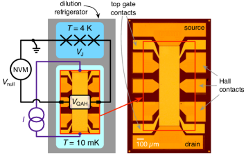
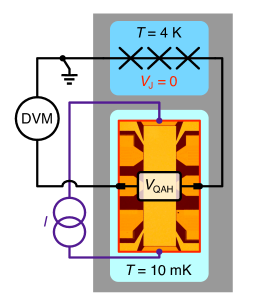
A schematic depicting the conceptual design of the QCS is shown in Fig. 1 (left). The current to be determined, , biases an ideal QAH resistor to generate a transverse voltage . Simultaneously, junctions of a PJVS are biased at a microwave frequency to be on their first Shapiro steps, yielding a voltage across the array [11, 36, 37, 38]. is tied to the high-potential side of the QAH Hall bar so that the potential difference can be measured by a nanovoltmeter at room temperature. For a given value of , if is tuned such that the current is known to be
| (1) |
Here the subscript ‘direct’ is used to indicate that this measurement is a ‘direct realization’ of the ampere — i.e. the measurement of is done through the integration of two quantum standards, without the use of any transfer standards, in a manner consistent with the definition of the ampere.
Generalizing to the case of nonzero null voltage and imperfect quantization of the QAH resistor, the current can still be calculated according to
| (2) |
is the measured transverse-resistance of the QAH device when it is biased with current and the PJVS is biased with frequency .
Radiative leakage of the microwave bias for the PJVS (mounted at the 4K stage) may result in undesirable electromagnetic coupling to other parts of the cryostat. In our realization of the QCS, such coupling resulted in electron heating of the QAH device (connected to the lowest-temperature stage) and was determined to be the main source of deviation of Hall resistance from quantization (see Fig. E1 in the Extended data section). By limiting to specific frequencies and measuring quantization of the QAH device for each value of in situ (see Methods) the impact of radiative leakage on QCS performance was made minimal. Details of the impact of leakage on the QAH device can be found in the Supplemental Information.
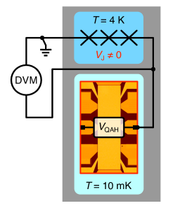
In addition to functioning as a novel realization of the ampere as discussed above, the QCS can also function as a current detector. To verify the QCS as an accurate current detector, a second measurement of is made in a standard Ohm’s law configuration. Here, still biases the QAH device as in Fig. 1, but the microwave bias to the PJVS is disabled and the Josephson junction array functions as a superconducting short on-chip ( V). A Keysight 3458A digital voltmeter, previously calibrated against the PJVS, is used to measure the Hall voltage . The current is then calculated according to
| (3) |
and compared to . Agreement of the two measurements indicates that the QCS can accurately determine the magnitude of and therefore functions as a novel current sensor, as well as a realization of the ampere. A simplified schematic depicting the measurement of and the calibration of the DVM can be found in the Supplemental Information.
A dry 3He/4He dilution refrigerator housed both the PJVS and QAH devices. The PJVS was mounted on the 4 K stage and covered by a Cu radiation shield to minimize stray microwave leakage to the QAH sample. The QAH device was mounted to a sample stage at the end of a cold finger below the mixing chamber plate. Base temperature at the sample stage was approximately 10 mK, as measured by a ruthenium oxide resistance thermometer. Direct current (DC) wiring to the QAH sample and to the PJVS consisted of copper twisted pair embedded within a woven loom. Each 12-pair cryogenic woven loom cable was broken by mating pairs of 25-pin micro-D connectors at the 60 K, 4 K, and mixing chamber temperature stages to aid in thermalization.
Equations (1) and (2) imply that the QCS’s uncertainty directly depends on the quality of quantization of the quantum anomalous Hall resistance to and Josephson voltage to . Deviation of from is known to vary with both current bias and electron temperature [31, 32, 33, 39, 34]. To account for this we measure the quantization of the QAH resistor for each value of and in situ. The quantized voltage of the PJVS is also verified in situ. Details of the independent characterizations of the PJVS and a QAH resistor can be found in the Methods section, with extended details available in the Supplemental Information.
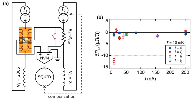
For this work we used the 16-bit digital current source of a commercial cryogenic current comparator [40, 41, 42] to provide the longitudinal current bias to the QAH device. A cryogenic current comparator is a standard instrument within the field of electrical metrology[43, 44] and is commonly used for precision measurements of resistance [6, 44]. The cryogenic current comparator’s current source was used for in situ characterization of the Hall resistance in a bridge configuration (the most common use of a cryogenic current comparator). The cryogenic current comparator’s current source was also used to bias the QAH device during direct and indirect measurements. The nominal output of the current source was set using the cryogenic current comparator’s graphical user interface (GUI). Onward, the cryogenic current comparator’s digital current source will be referred to simply as the ’current source’
III. Results and Discussion
The QCS has two main functions: (1) serving as realization of the ampere and (2) acting as a novel form of current sensor that is capable of measuring an unknown current. Below we highlight the subtle aspects that make these two functionalities distinct despite their near-identical implementation, and we assess the performance of the QCS in each mode.
As noted in the introduction, realization of a unit requires that a quantity of the same kind as a unit, in this case an electrical current, be given a value and associated uncertainty in a manner consistent with the unit’s definition. Realization of the ampere has previously been achieved by applying Ohm’s law to realizations of the SI derived units the volt and the ohm, based on the Josephson effect and QH effect respectively. The QAH effect has emerged as a viable replacement for the QH effect as a realization of the ohm [27], and could play that role in realization of the ampere.
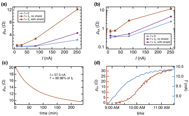
To establish a new realization of the ampere we first characterized the PJVS and the QAH devices to confirm that they functioned as realizations of the volt and the ohm, respectively, when placed in the QCS configuration (see Methods). Next, we demonstrated that we could combine these components to associate a value (and uncertainty) with an electrical current — as is required to claim realization of the ampere. Using the current source’s GUI we directed the digital current source to output a specific current which was used to bias the QAH device. We chose in succession 11 different current values between nA and nA. In each case, we biased junctions on the PJVS with the appropriate microwave bias frequency (either or depending on the value of — see Supplemental Information) to be on their first Shapiro steps and hence to nearly match the voltage expected across the QAH device. was then measured as shown in Fig. 1 .
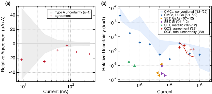
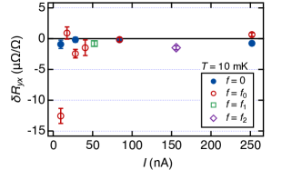
To eliminate thermoelectric offsets in the polarity of the input current was reversed periodically during the measurement. At least 760 samples of were averaged across at least 10 (up to 90) of these polarity reversal cycles, with each cycle lasting an average of 60 s. The final averaged value of was used, along with the corresponding value of , to determine the magnitude of according to equation (2). The relative combined uncertainty (, corresponding to a 68% confidence interval) for these measurements is shown as a solid red trendline in Fig. 2(b). The combined uncertainty was calculated as a root sum of squares of the Type A and Type B contributions (see Section IV for a full discussion of the uncertainty budget).
The measurements discussed above constitute a novel realization of the ampere and, on their own, serve as a significant accomplishment in the field of electrical metrology. Indeed, the relative uncertainty for current detection using the QCS meets or exceeds that available using state-of-the-art calibration and measurement capabilities from national metrology institutes around the world (see Fig. 2(b) — a full discussion of this figure to follow) in this current range. However, to be of practical use for national metrology institutes, this realization should perform as well as or better than existing methods used for measuring an electrical current. It is ultimately the accuracy of the QCS that distinguishes functionalities (1) and (2).
To assess the accuracy of the QCS, additional measurements of were made in a traditional Ohm’s law configuration as described in Section II. The same 11 values of current (indicated by the current source’s GUI) were sourced and the value of was calculated using equation (3). These measured values were then compared to the corresponding measurement of .
Figure 2(a) shows , the relative agreement of the two current measurements, as red markers. The combined Type A uncertainties () of the two measurements ( and ) is shown as a shaded region centered around 0 AA. This combined uncertainty was calculated as an root-sum-square total of the individual Type A uncertainties. Values of within 400 AA of one another have been grouped into a single data point. A table showing the exact GUI setting for , and the corresponding, individually-measured values of and , can be found in the Supplemental Information.
If statistical uncertainty were the only factor contributing to the differences between the measurements of and , then their relative agreement should fall within the combined Type A uncertainty as is the case for nA and nA. Here it is important to note that the uncertainty budget is dominated by Type A contributions to the extent that Fig. 2(a) would remain visually unchanged if Type B (non-statistical) uncertainties shown in Section IV were included. (The full uncertainty budget for can be found in Section IV and the uncertainty budget for can be found in the Supplemental Information.) The fact that the relative agreement falls outside the combined Type A uncertainty for nA, 51.9 nA, 132 nA, and 252 nA could mean that the Type A uncertainty for one or both measurements was under-evaluated or that a relatively large non-statistical source of error was unaccounted for in the budget. Measurements made in close succession were highly repeatable (see Section IV) and so the latter possibility is far more likely.
We believe that the observed disagreement was caused by long-term drift in the output of the current source. Multiple measurements of were taken over the course of 8 days. During this time we observed that the measured value of differed by a relative amount of 28.0 AA for the same GUI setting of nA (see Supplemental Information). Importantly, this difference is greater than the average disagreement between direct and indirect current measurements at any value of .
Due to experimental constraints, measurements of and were taken more than 1 week apart. Given the evidence of drift discussed above, we conclude that despite the settings on the digital current source being the same between measurements of and for a given value of , the magnitude of the current source’s output likely drifted between those two measurements, inflating the disagreement to be outside of their combined uncertainty. Because the error due to drift is an artifact of the particular current source being measured and not something fundamental to the QCS, it has not been included in our error budget. This level of drift is not a reflection of the quality of the current source nor is it an issue that would have been noticed during normal operation of the cryogenic current comparator. This is because long-term stability of a cryogenic current comparator’s current source is not a necessary design criterion for that instrument given the compensation network and the balancing procedure used in typical bridge comparisons. A detailed discussion of this topic can be found in the Supplemental Information.
Fig. 2(b) contextualizes our realization of the ampere by the QCS amongst the best realizations and calibration and measurement capabilities reported by national metrology institutes worldwide. State-of-the-art calibration and measurement capabilities from the Physikalisch-Technische Bundesanstalt (PTB) and the Istituto Nazionale di Ricerca Metrologica (INRIM) using an ultrastable low-noise current amplifier (ULCA) [45] (blue diamond markers), as well as calibration and measurement capabilities based on the traditional Ohm’s law method (shaded region) [45] are shown across a broad current range of currents. The list of institutes referenced by shaded region can be found in the Supplemental Information. Several realizations of the ampere are also shown. Metallic [15, 16] (green triangles), GaAs [17, 18, 19] (orange triangles), and silicon [20, 21, 22] (purple triangles) SET devices are shown in the fA to nA region. For direct comparison to the other data shown, the relative uncertainty of our QCS measurements are depicted as a solid red trendline. We also plot the relative agreement of with from Fig. 2(a) as red crosses. For a given value of current, the larger of these two values (QCS agreement or QCS uncertainty) can be viewed as a ‘worst-case scenario’ for performance of the QCS. Even when assessed in this manner, our measurements meet or exceed the precision offered by state-of-the-art calibration and measurement capabilities for all values of current tested. Not shown in Fig. 2(b) are the results of the three-cryostat integration of a Josephson voltage standard with QH resistance standard where a relative uncertainty of A/A was obtained for currents in the mA range [27].
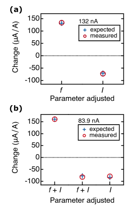
Additional measurements of were made to check the accuracy and overall performance of the QCS in response to small variations of the input parameters and , an example of which is shown in Fig. 3(a). For these measurements, a nominal current of nA was set using the current source’s GUI and a standard measurement of was performed. Immediately following this measurement, the bias current was decreased by the smallest allowed step on the GUI so that the new nominal current value was nA — a relative change of roughly AA. The measurement of was then repeated. The measurement relative difference between these two measurements of is shown as a red circular marker in Fig. 3(a), the expected relative change based on the difference between the two nominal values of indicated by the GUI setting is shown as a blue cross.
A similar procedure was repeated using as the varied parameter. Again, an initial measurement of was made with the nominal bias current 132.3984 nA. Immediately after this measurement the bias frequency was changed and was calculated such that the resulting relative change in was approximately 130 AA ( and are the changes in the null voltage and frequency respectively). The expected change is shown as a blue cross in Fig. 3(a). This change in was small enough that the value of was unaffected. Measurement of was then repeated. The measured change in is shown as a red, circular marker Fig. 3(a).
When either or was adjusted, the measured change in () was equal, within uncertainty, to the expected change. A similar set of measurements were repeated when the nominal current set by the GUI was nA. In addition to varying or alone, these tests also included combined variations of both parameters, . Again, the measured and expected changes were equal for all cases.
The measurements described above have implications when assessing functionalities (1) and (2) of the QCS. In the case of (1) these measurements definitively show that the PJVS and QAH device are directly integrated with one another during operation of the QCS. If this was not the case, and the devices were independent from one another, varying while keeping the magnitude of the bias current constant would not result in a measurable change that is consistent with the predicted value. Regarding functionality (2), it is important to note that the these measurements were done using one value of current where the relative agreement of and fell within their combined uncertainty ( nA) and one current where the relative agreement was outside the combined uncertainty ( nA). Despite this, measured changes in matched the expected change in either case. Though the changes in shown here were larger than the disagreement between and , these measurements still demonstrate that the QCS is able to accurately detect small variations in current even for those values of where comparisons of with suggest the possibility of diminished accuracy (again, we believe this disagreement is a result of uncontrollable drift of the current source over time).
IV. Uncertainty Budget
The overall uncertainty budget for the QCS data shown in Fig. 2(a) is given in Table 1. The dominant contribution is that due to statistical fluctuations of the nanovoltmeter readings of . This Type A contribution , is defined as the standard deviation of means of multiple polarity reversals within a single experimental run. For all direct measurements, nV, which is close to the noise floor for our measurement system. Thus, since we are noise-limited, the relative uncertainty decreases as the magnitude of the bias current increases. This is illustrated in Table 1: the lowest (highest) relative Type A uncertainties correspond to the highest (lowest) value of the bias current .
Type B contributions include: offsets to measurements of due to the finite input impedance, gain and linearity of the nanovoltmeter (referred to as NVM in the table), uncertainty of the tone used for PJVS microwave bias frequency , and the combined uncertainty associated with measurement of . The total root-sum-square (RSS) combined uncertainty () is given in the final row of the table. A detailed description of each uncertainty source can be found in the Supplemental Information.
| Source | Type | Contribution |
| Null detector reading11footnotemark: 1 | A | 2.3 – 40.0 |
| quantization | A+B | 1.0 |
| NVM input impedance | B | 3.0 |
| NVM gain & linearity | B | 0.001 |
| PJVS microwave bias | B | 0.001 |
| Total11footnotemark: 1 | RSS | 3.91 – 41.2 |
1For currents ranging from nA to nA.
Whereas the contribution of the null voltage fluctuations range from 2.4 AA to 40 AA, multiple measurements at the same nominal current (i.e., same GUI setting) are highly repeatable, particularly at the highest currents. For different evaluations of the relative difference of the means ranged from 1.0 AA at nA to AA at nA. To gain a more complete understanding of the factors contributing to our noise floor, we independently measured the Allan deviation for different experimental configurations of the nanovoltmeter in a separate laboratory. (A detailed discussion of the Allan deviation calculations can be found in the Supplemental Information.) In one configuration, we shorted the nanovoltmeter terminals together using a ‘low thermal EMF’ plug provided by the manufacturer that connects directly to the nanovoltmeter’s input connector. In another, we shorted the copper spade terminals together at the end of the low-thermal cable that is furnished with the nanovoltmeter.
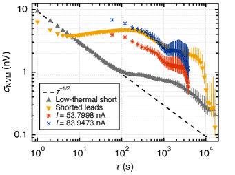
The Allan deviations for both measurements as a function of are shown on a - scale in Fig. 4. The ‘low-thermal short’ data, can be viewed as a baseline contribution of the nanovoltmeter to the overall stability and noise of the measurement setup. For s, the data clearly scale as indicating a white-noise-dominated spectrum [46]. For longer times, the influence of the finite sampling time (evidenced by the rapid growth in the uncertainty of ) and of noise with different spectra can be seen. Comparing this measurement to that done with the shorted, low-thermal cable (‘shorted leads’) is particularly enlightening. Here the initial magnitude of is smaller and the spectrum again appears white noise dominated. However, this functional behavior quickly transitions to a spectrum more similar to that of noise where is approximately constant, before eventually ( s) transitioning back to a seemingly white-noise-dominated spectrum.
Comparing the ‘shorted leads’ Allan deviation trend to that of QCS data at nA and nA suggests that the cabling needed to connect the nanovoltmeter to the devices in the fridge introduces a sizable amount of noise to the QCS measurements. The magnitude and functional form of the QCS Allan deviation is comparable to that when the leads were shorted with the 1 m cable. The variation in magnitude depicted around s between the two QCS measurements is similar to that observed between multiple measurements of the shorted leads. Thus, even though a longer length of cable (internal and external to fridge) was required to obtain the QCS data, one should not necessarily expect the QCS Allan deviation to always exceed that of the ‘shorted leads’ case because of the variability between different Allan deviation measurements. The variability is likely due to changes in the lab environment — for example, microphonic and/or electromagnetic pickup from adjacent experiments or occupants. These results suggest that uncertainty reductions may be possible in future QCS measurements by meticulous design of experimental wiring.
V. Conclusions
We have successfully integrated a PJVS and QAH resistance standard within a single cryostat to realize the quantum ampere for currents within the range 9.33 nA to 252 nA. For the range of currents tested, the uncertainty of the measurements made by this first iteration of the QCS meet or exceed what is currently offered worldwide by national metrology institutes today. Furthermore, the QCS stands as one of the only realizations of the ampere within the range of A to A.
By conducting a comprehensive analysis of the uncertainty budget and noise spectra associated with the QCS measurements, we were able to establish definitive routes for improving future iterations of the QCS design. Improving the electromagnetic shielding and filtering for both the QAH device and the PJVS would allow the bias frequency to be continuously adjusted without needing to measure . Specialized wiring inside and outside the fridge would reduce the effects of triboelectric and thermoelectric noise sources. A wider Hall bar structure should increase the operating range of the QCS to currents beyond 250 nA. Finally, assuming a predominantly white noise spectrum, significantly increased measurement times should greatly reduce Type A uncertainty.
Having demonstrated that the QCS is capable of measuring an electrical current with roughly the same precision and accuracy as a traditional Ohm’s law measurement, future implementations need not be limited to a single current source. However, follow-up measurements of the cryogenic current comparator’s digital current source used here may be done to provide additional confirmation of long-term drift.
Finally, the development of novel realizations of the SI base and derived units — especially realizations that utilize quantum phenomena — was an initiative set by the General Conference on Weights and Measures during the 2019 redefinition of the SI. In keeping with this initiative, it is our hope that the design and methodology presented here can be adapted and enhanced to further improve and diversify the field of electrical metrology.
Methods
PJVS device and characterization: The PJVS device used in this work was based on the same triple-stacked, Nb/NbSix/Nb junction process used in NIST’s Standard Reference Instruments [47, 48]. The cryopackaged chip contains 59,140 junctions and is capable of an output voltage of approximately 2 V at a microwave bias frequency of 18 GHz. The junctions are arranged into two symmetric arrays and share a common microwave bias, which is distributed using on-chip microwave splitters. This allows the chip to be operated as a dual-channel (1 V + 1 V) source and is the configuration used in this work. Each array is further divided into ternary-weighted subarrays.
It is well established [49] that PJVSs can suffer diminished critical currents and/or operating margins when subjected to magnetic fields. In some instances, the effect may be reversed once the field is removed. But certain scenarios result in an irreversible loss of quantization. For the latter, quantization can be restored by briefly increasing the temperature of the PJVS to above the critical temperature of Nb. To account for this possibility, a heater was attached to the fridge’s 4 K stage and operated in an open-loop manner.
To assess the performance of the PJVS in the environment of the fridge, we swept the field of the fridge’s solenoid magnet up to 1 T (within solenoid) and measured the stray field outside the vacuum envelope, but near the PJVS (the radial separation between PJVS and probe was approximately 10 cm). For a 1 T solenoid field, we measured a stray field magnitude of approximately 1 mT near the cryopackage, a value which is consistent with the known field map of the bare solenoid (with integrated bucking coil) and the passive shielding added by the fridge’s manufacturer (no additional magnetic shielding was installed around the PJVS cryopackage). We also monitored the critical current and Shapiro step width of one of the 8 400-junction subarrays for a bias frequency of 9.7 GHz. At the maximum 1 T field, we found no observable change in the PJVS critical current or Shapiro step width.
To allow comparison to historical performance at liquid helium temperatures, we heated the fridge’s 4 K stage to approximately 4.2 K. The critical current and Shapiro step widths were comparable to those measured in liquid helium: mA, mA for the fridge at 9.7 GHz and approximately 4 K, compared with mA, mA at 18 GHz in liquid helium. The difference in step width could be due to the response of the junction array vs frequency or the fact that the power amplifier used in this work has a lower maximum output power. During the field sweep, we did observe a slight decrease in critical current each time the field was stepped. Since we also observed increases in the temperature of the 4 K stage at each field increment, we attribute the reduction in critical current to changes in temperature, rather than a direct result of the field itself.
QAH film composition and device fabrication: The QAH insulator sample studied in this was work was a high quality, 6-quintuple-layer (QL) Cr-doped (Bi,Sb)2Te3 thin film grown by molecular beam epitaxy on a semi-insulating GaAs (111)B substrate. The first and sixth QLs featured increased Cr concentration, (Cr0.24Bi0.26Sb0.62)2Te3, compared to the inner four QLs, (Cr0.12Bi0.26Sb0.62)2Te3. A lock-in characterization of the QAH state of this film is given in the Supplemental Information.
The 300 m wide Hall bar used in this study (Fig. 1) was fabricated using a combination of photolithography, metal evaporation, wet and dry etching and atomic layer deposition. Prior to all photolithography steps, the chip was cleaned in acetone and isopropyl alcohol, coated in SPR 3612 photoresist (spun at spun at 5.5 krpm for 45 s) and baked at 80 °C for 2 minutes. After exposure, the resist was developed in a phosphate salt developer followed by two water rinses (extended fabrication details can be found in the Supplemental Information).
Each pair of Hall contacts was separated by a lateral, center-to-center distance of 300 m. The device featured a top gate (40 nm alumina dielectric covered by a Ti/Au electrode) for tuning the chemical potential in the film. However, measurements of the longitudinal resistance as a function of gate voltage indicated that the native Fermi level was well positioned near the center of the exchange gap (see Supplemental Information). Therefore, all measurements were taken with 0 V applied to the top gate.
QAH characterization: Prior to characterization, the QAH device was magnetized by applying a 1 T out-of-plane magnetic field and then reducing the field to 0 T.
To characterize the QAH device, quantization of the Hall resistance relative to , , was measured as a function of bias current and PJVS microwave bias frequency , using a cryogenic current comparator. All measurements took place with the cryostat operating at base temperature base temperature with mK at the sample stage. Extensive details of the methodology used to measure and an estimation of the uncertainty budget for the same cryogenic current comparator and measurement set-up, can be found in previous publications [31, 33] as well as in the Supplemental Information.
Measurements of as a function of were first done with the microwave excitation to the PJVS turned off (), as a baseline measure of sample quality. The measurements were then repeated with the microwave excitation to the PJVS turned on but with the PJVS inactive (i.e. but V). This was done to simulate the environment that the QAH device would experience while being used in the QCS configuration. By comparing these two sets of measurements, the effects of microwave leakage to the QAH sample could be qualified. Indeed, it was found that certain frequencies caused large deviations from baseline behavior, whereas others had only moderate effects (full discussion on this topic can be found in the Supplemental Information). As a result, unless otherwise stated, all measurements taken with the microwave excitation turned on were done so at one of three fixed frequencies (0 dBm): GHz, GHz, or GHz. These frequencies were shown to have only modest impact on the quantization of the QAH device. A table showing which of the three frequencies were used during each QCS measurement of is given in the Supplement Information. The measured values of are shown Fig. E1 of the Extended Data section.
Extended Data
Supplementary information
See supplementary material for full details regarding: independent characterizations of the digital voltmeter, the QAH device (film growth, extended fabrication details, and longitudinal resistivity measurements as a function of top gate voltage) and QCS measurement protocols. Also included are names of the national metrology institutes referenced for calibration and measurement capability data, the indirect current measurement schematic, evidence of long term drift of the cryogenic current comparator’s digital current source, a discussion on the impacts of the heating due to microwave leakage, and details on changes to the internal wiring of the dilution refrgerator to facilitate in situ characterization and QCS measurements during a single cooldown, tables detailing how measurements of , correspond to the GUI setting of , evidence of radiative heating of the QAH device via microwave leakage, and Allan deviation calculations.
Acknowledgments The authors thank T. Mai, F. Fei, G. J. Fitzpatrick, and E. C. Benck for assistance with the NIST internal review process. The authors also thank Ilan T. Rosen and Marc A. Kastner for enlightening discussions throughout this work. L.K.R., M.P.A. and D.G.-G. were supported by the Air Force Office of Scientific Research (AFOSR) Multidisciplinary Research Program of the University Research Initiative (MURI) under grant number FA9550-21-1-0429. At the initiation of the project L.K.R., M.P.A. and D.G.-G. were supported by the U.S. Department of Energy, Office of Science, Basic Energy Sciences, Materials Sciences and Engineering Division,under Contract No. DE-AC02-76SF00515 and the Gordon and Betty Moore Foundation through Grant No. GBMF9460. P.Z., L.T. and K.L.W. acknowledge the support from the National Science Foundation (NSF) (DMR-1411085 and DMR-1810163) and the Army Research Office MURI under grant numbers W911NF16-1-0472 and W911NF-19-S-0008. Commercial equipment, instruments, and materials are identified in this paper in order to specify the experimental procedure adequately. Such identification is not intended to imply recommendation or endorsement by the National Institute of Standards and Technology or the United States government, nor is it intended to imply that the materials or equipment identified are necessarily the best available for the purpose. Work presented herein was performed, for a subset of the authors, as part of their official duties for the United States government. Funding is hence appropriated by the United States Congress directly. Part of this work was performed at nano@stanford, supported by the National Science Foundation under award ECCS-2026822.
References
- [1] Ian M Mills et al. “Redefinition of the kilogram: a decision whose time has come” In Metrologia 42.2 IOP Publishing, 2005, pp. 71
- [2] Martin JT Milton et al. “Towards a new SI: a review of progress made since 2011” In Metrologia 51.3 IOP Publishing, 2014, pp. R21
- [3] Richard Davis “An introduction to the revised international system of units (SI)” In IEEE Instrum. Meas. Mag. 22.3 IEEE, 2019, pp. 4–8
- [4] Wilfrid Poirier et al. “The ampere and the electrical units in the quantum era” In C. R. Phys. 20.1-2 Elsevier, 2019, pp. 92–128
- [5] David B Newell et al. “The international system of units (SI)” In NIST Special Publication 330, 2019, pp. 1–138
- [6] Beat Jeckelmann et al. “The quantum Hall effect as an electrical resistance standard” In Rep. Prog. Phys. 64.12 IOP Publishing, 2001, pp. 1603
- [7] Félicien Schopfer et al. “Quantum resistance standard accuracy close to the zero-dissipation state” In J. Appl. Phys. 114.6 American Institute of Physics, 2013, pp. 064508
- [8] Alexander Tzalenchuk et al. “Towards a quantum resistance standard based on epitaxial graphene” In Nat. Nanotechnol. 5.3 Nature Publishing Group UK London, 2010, pp. 186–189
- [9] R Ribeiro-Palau et al. “Quantum Hall resistance standard in graphene devices under relaxed experimental conditions” In Nat. Nanotechnol. 10.11 Nature Publishing Group UK London, 2015, pp. 965–971
- [10] Albert F Rigosi et al. “The quantum Hall effect in the era of the new SI” In Semicond. Sci. Technol. 34.9 IOP Publishing, 2019, pp. 093004
- [11] WK Clothier et al. “A determination of the volt” In Metrologia 26.1 IOP Publishing, 1989, pp. 9
- [12] F Bloch “Josephson effect in a superconducting ring” In Phys. Rev. B 2.1 APS, 1970, pp. 109
- [13] T. A. Fulton “Implications of Solid-State Corrections to the Josephson Voltage-Frequency Relation” In Phys. Rev. B 7 American Physical Society, 1973, pp. 981–982
- [14] BN Taylor et al. “New international electrical reference standards based on the Josephson and quantum Hall effects” In Metrologia 26.1 IOP Publishing, 1989, pp. 47
- [15] Mark W Keller et al. “Uncertainty budget for the NIST electron counting capacitance standard, ECCS-1” In Metrologia 44.6 IOP Publishing, 2007, pp. 505
- [16] Benedetta Camarota et al. “Electron Counting Capacitance Standard with an improved five-junction R-pump” In Metrologia 49.1 IOP Publishing, 2011, pp. 8
- [17] SP Giblin et al. “Towards a quantum representation of the ampere using single electron pumps” In Nat. Commun. 3.1 Nature Publishing Group UK London, 2012, pp. 930
- [18] Friederike Stein et al. “Validation of a quantized-current source with 0.2 ppm uncertainty” In Appl. Phys. Lett. 107.10 AIP Publishing, 2015
- [19] Myung-Ho Bae et al. “Precision measurement of single-electron current with quantized Hall array resistance and Josephson voltage” In Metrologia 57.6 IOP Publishing, 2020, pp. 065025
- [20] Gento Yamahata et al. “Gigahertz single-electron pumping in silicon with an accuracy better than 9.2 parts in 107” In Appl. Phys. Lett. 109.1 AIP Publishing, 2016
- [21] R Zhao et al. “Thermal-error regime in high-accuracy gigahertz single-electron pumping” In Phys. Rev. Appl. 8.4 APS, 2017, pp. 044021
- [22] Stephen Giblin et al. “Precision measurement of an electron pump at 2 GHz; the frontier of small DC current metrology” In Metrologia, 2023
- [23] Atsushi Domae et al. “Experimental demonstration of current dependence evaluation of voltage divider based on quantized Hall resistance voltage divider” In IEEE Trans. Instrum. Meas. 66.6 IEEE, 2017, pp. 1237–1242
- [24] Eite Tiesinga et al. “CODATA recommended values of the fundamental physical constants: 2018” In Rev. Mod. Phys. 93 American Physical Society, 2021, pp. 025010
- [25] Hansjörg Scherer et al. “Quantum metrology triangle experiments: a status review” In Meas. Sci. Technol. 23.12 IOP Publishing, 2012, pp. 124010
- [26] Mark W Keller “Current status of the quantum metrology triangle” In Metrologia 45.1 IOP Publishing, 2008, pp. 102
- [27] J Brun-Picard et al. “Practical quantum realization of the ampere from the elementary charge” In Phys. Rev. X 6.4 APS, 2016, pp. 041051
- [28] YL Chen et al. “Massive Dirac fermion on the surface of a magnetically doped topological insulator” In Science 329.5992 American Association for the Advancement of Science, 2010, pp. 659–662
- [29] Rui Yu et al. “Quantized anomalous Hall effect in magnetic topological insulators” In Science 329.5987 American Association for the Advancement of Science, 2010, pp. 61–64
- [30] Joseph G Checkelsky et al. “Dirac-fermion-mediated ferromagnetism in a topological insulator” In Nat. Phys. 8.10 Nature Publishing Group UK London, 2012, pp. 729–733
- [31] Eli J Fox et al. “Part-per-million quantization and current-induced breakdown of the quantum anomalous Hall effect” In Phys. Rev. B 98.7 APS, 2018, pp. 075145
- [32] Martin Götz et al. “Precision measurement of the quantized anomalous Hall resistance at zero magnetic field” In Appl. Phys. Lett. 112.7 AIP Publishing, 2018
- [33] Linsey K. Rodenbach et al. “Metrological Assessment of Quantum Anomalous Hall Properties” In Phys. Rev. Appl. 18 American Physical Society, 2022, pp. 034008
- [34] Yuma Okazaki et al. “Quantum anomalous Hall effect with a permanent magnet defines a quantum resistance standard” In Nat. Phys. 18.1 Nature Publishing Group UK London, 2022, pp. 25–29
- [35] Molly P Andersen et al. “Low-damage electron beam lithography for nanostructures on Bi2Te3-class topological insulator thin films” In J. Appl. Phys. 133.24 AIP Publishing, 2023
- [36] WC Stewart “Current-voltage characteristics of Josephson junctions” In Appl. Phys. Lett. 12.8 American Institute of Physics, 1968, pp. 277–280
- [37] Richard Kautz “Design and Operation of Series-Array Josephson Voltage Standards” Proc. Intl. School of Physics Enrico Fermi Course CX Villa Marigola IT, 1992
- [38] Richard L Kautz “Shapiro steps in large-area metallic-barrier Josephson junctions” In J. Appl. Phys. 78.9 American Institute of Physics, 1995, pp. 5811–5819
- [39] Ilan T. Rosen et al. “Measured Potential Profile in a Quantum Anomalous Hall System Suggests Bulk-Dominated Current Flow” In Phys. Rev. Lett. 129 American Physical Society, 2022, pp. 246602
- [40] Martin Gotz et al. “Improved cryogenic current comparator setup with digital current sources” In IEEE Trans. Instrum. Meas. 58.4 IEEE, 2009, pp. 1176–1182
- [41] D Drung et al. “Improving the stability of cryogenic current comparator setups” In Supercond. Sci. Technol. 22.11 IOP Publishing, 2009, pp. 114004
- [42] Dietmar Drung et al. “Aspects of application and calibration of a binary compensation unit for cryogenic current comparator setups” In IEEE Trans. Instrum. Meas. 62.10 IEEE, 2013, pp. 2820–2827
- [43] DB Sullivan et al. “Low temperature direct current comparators” In Rev. Sci. Instrum. 45.4 American Institute of Physics, 1974, pp. 517–519
- [44] JM Williams “Cryogenic current comparators and their application to electrical metrology” In IET Sci. Meas. Technol. 5.6 IET, 2011, pp. 211–224
- [45] BIPM “Calibration and Measurement Capabilities Electricity and Magnetism: DC current (low and intermediate values)” URL: https://www.bipm.org/kcdb/
- [46] David W Allan “Should the classical variance be used as a basic measure in standards metrology?” In IEEE Trans. Instrum. Meas. IEEE, 1987, pp. 646–654
- [47] Anna E Fox et al. “Junction yield analysis for 10 V programmable Josephson voltage standard devices” In IEEE Trans. Appl. Supercond 25.3 IEEE, 2014, pp. 1–5
- [48] NIST “SRI 6000 Series Programmable Josephson Voltage Standard (PJVS), https://www.nist.gov/sri/standard-reference-instruments/sri-6000-series-programmable-josephson-voltage-standard-pjvs”
- [49] Anna E Fox et al. “Induced Current Effects in Josephson Voltage Standard Circuits” In IEEE Trans. Appl. Supercond. 29.6 IEEE, 2019, pp. 1–8
Supplemental information for: Realization of the quantum ampere using the quantum anomalous Hall and Josephson effects
Linsey K. Rodenbach1,2,3†, Ngoc Thanh Mai Tran3,4†, Jason M. Underwood3†, Alireza R. Panna3, Molly P. Andersen2,5, Zachary S. Barcikowski3,4, Shamith U. Payagala3, Peng Zhang6, Lixuan Tai6, Kang L. Wang6, Randolph E. Elmquist3, Dean G. Jarrett3, David B. Newell3, Albert F. Rigosi3 and David Goldhaber-Gordon1,2a
1Department of Physics, Stanford University, Stanford, California 94305, USA
2Stanford Institute for Materials and Energy Sciences, SLAC National Accelerator Laboratory, 2575 Sand Hill Road, Menlo Park, California 94025, USA
3Physical Measurement Laboratory, National Institute of Standards and Technology (NIST), Gaithersburg, Maryland 20899, USA
4Joint Quantum Institute, University of Maryland, College Park, Maryland 20742, USA
5Department of Materials Science and Engineering, Stanford University, Stanford, California 94305, USA
6Department of Electrical and Computer Engineering, Department of Physics and Astronomy, University of California, Los Angeles, Los Angeles, California 90095, USA
†These authors contributed equally to this work.
aTo whom correspondence should be addressed; E-mail: goldhaber-gordon@stanford.edu
S1 Indirect Current Measurement Schematic
Fig. S1 depicts the of the Ohm’s law based current measurement used to determine . The current was generated using the cryogenic current comparator’s (CCC) digital current source as discussed in the main text.
S2 Independent Characterizations
S2.1 Digital voltmeter characterization
Measurements of require both a quantized and a sufficiently characterized voltmeter to enable accurate measurements of the transverse voltage . We used the same programmable Josephson voltage standard (PJVS) array located at the dilution refrigerator’s (DR) 4 K stage to characterize the digital voltmeter (DVM), as shown in Fig. S2. This was facilitated by a separate set of voltage leads that run from the cryopackage directly to room-temperature connections (i.e., is not in the measurement loop). We set the PJVS voltage to the nominal values used in the direct measurements and compared the calculated (expected) voltage with the DVM’s measurement. The purpose here was to check that the error was within an acceptable range—less than the measurement’s Type A uncertainty and less than the overall uncertainty of the direct measurements alone. This condition was satisfied for all voltages considered.
Additional sources of error include the input resistance of the DVM and the interaction of the DVM’s pumpout current with resistances in the measurement circuit (e.g., , RC filtering, or wiring). We characterized both of these phenomena in separate measurements in a different lab. For the DVM’s 100 mV range, we found the input resistance was greater than 1 T. Pumpout current associated with the DVM’s autozero cycle can be mitigated by disabling autozero. However, we found that this increased the Type A uncertainty of the measurements. Even though our indirect measurements incorporated current reversals, these would not correct for the DVM’s internal drift. Instead, we added a delay between the autozero and the start of the DVM’s integration cycle to ensure that residual pumpout currents are negligible.
S2.2 Extended discussion: QAH characterization
From the Methods section of the main text: prior to characterization, the quantum anomalous Hall (QAH) device was magnetized by applying a 1 T out-of-plane magnetic field and then reducing the field to 0 T.
To characterize the QAH device, quantization of the Hall resistance relative to , , was measured using commercial CCC resistance bridge – designed by Physikalisch-Technische Bundesanstalt (PTB) and manufactured by Magnicon [S1–S3]. A general description of the methodology used to measure is given below but extensive details can be found in previous publications by Fox, et al. [S4] and Rodenbach, et al. [S5], both of whom used the CCC from this work to characterize the Hall resistance of similar QAH samples.
A simplified schematic depicting how the CCC was used in the measurement of is shown in Fig. S3(a). The main components of the CCC are: two low-noise digital current sources, and , used to source currents across two resistors that are to be compared, and ; a nanovoltmeter (NVM) used to measure the difference in the potential drops across the the two resistors; two sets of superconducting windings, and , which are housed in a superconducting toroidal screen (not pictured); and a superconducting quantum interference device (SQUID) to which the windings are inductively coupled.
The CCC works by comparing an unknown resistance to one that is precisely known. In this case, is the unknown resistance which is biased by current source . The known resistor, biased by current source , was chosen to be NIST’s 100 calibrated standard resistor () with a known drift of 32.7 n//year. The windings are chosen such that their ratio is as close as possible to the ratio of the resistors. In this work, windings and were chosen. As the two currents pass through their respective windings, any imbalance results in the presence of a net current on the surface of the superconducting screen due to the Meissner effect. The surface current produces a magnetic flux that can be measured by the SQUID. This measurement is fed through a compensation network to produce a feedback signal that keeps the net flux constant and thereby holds the ratio of the two currents fixed. With the proper choice of and , the voltage drops across the resistors are approximately the same. The small difference in the two potential drops is measured with the NVM via . A precise measurement of the ratio of the two resistors is then obtained and the value of the unknown resistance can be determined.
To limit the the effects of thermal instability, was placed in a temperature-controlled oil bath. To eliminate thermoelectric offsets caused by linear thermal drift, the currents, and , reversed polarity every half-cycle (30 s). A total of 30 samples of were taken every half-cycle, the first 14 of which were ignored to allow for stabilization after current polarity reversal. Each measurements of consisted of at least 30 cycles.
The PJVS’s microwave bias frequency had no impact on the electrical set up shown in Fig. S3(a) or on the measurement procedure described above. The only effect of this bias was increasing the electron temperature of the QAH device (Section S5). This effect is undesirable and future implementations of the QCS will feature improved radiative shielding to mitigate microwave leakage.
Measurements of as a function of were first done with the microwave excitation to the PJVS turned off (), as a baseline measure of sample quality. The measurements were then repeated with the microwave excitation to the PJVS turned on but with the PJVS inactive (i.e. but V). This was done to simulate the environment that the QAH device would experience while being used in the QCS configuration. By comparing these two sets of measurements, the effects of microwave leakage to the QAH sample could be qualified. Indeed, it was found that certain frequencies caused large deviations from baseline behavior, while others had only moderate effects (full discussion on this topic can be found in Section S5). Furthermore, in some instances, the equilibration time of was found to be on the order of several hours, even for small () changes in . As a result, unless otherwise stated, all measurements taken with the microwave excitation turned on were done so at one of three fixed frequencies (0 dBm): GHz, GHz, or GHz, all three of which were shown have only modest impact on the quantization of the QAH device.For clarity, Table 3 in Section S4.2 shows which of the three frequencies were were used during each QCS measurement of .
Figure S3(b) shows the measurements of taken as a function of bias current, . When the microwave excitation was off (blue filled circles) for currents ranging from nA to nA. In comparison, when the microwave excitation to the PJVS turned on with (open markers), heating of the QAH device due to radiation leakage was observed as an increase in beyond the baseline value for a given . Regardless, for ,, or the deviations for all were small enough that they did not impact the overall function of the QCS (i.e. they are not the leading source of error). These deviations were taken into account during operation of the QCS though use of the measured value of as opposed to a fixed value of .
In summary, measurements of were made for all values of measured using the QCS. The frequency was one of the three found to have minimal heating effects ( GHz, GHz, or GHz). The particular choice of for a given was such that was as close as possible to (see Section S4.2). Figure S3(b) shows the measured values of used in this work. These values were used to compute the overall Hall resistance of the QAH device used in Eq. (2) of the main text via:
| (S1) |
S3 QAH Device and Measurements
S3.1 Extended details: QAH film growth and Hall bar fabrication
The Cr-doped (Bi,Sb)2Te3 (Cr-BST) material used in this work was grown on epi-ready semi-insulating GaAs (111)B substrate in an ultra-high vacuum, Perkin-Elmer molecular beam epitaxy (MBE) system. Before growth, the substrate was loaded into the MBE chamber and pre-annealed at a temperature of 630 °C in a Te-rich environment to remove the oxide on the surface. During growth, high-purity Bi, Sb, Cr and Te were evaporated from standard Knudsen cells. The substrate was kept at 200 °C. The reflection high-energy electron diffraction (RHEED) in situ was used to monitor the quality and thickness of the materials.
The Hall bar device (shown on the right in Fig. 1 of the main text) was fabricated using a combination of photolithography, metal evaporation, wet and dry etching and atomic layer deposition. Prior to all photolithography steps, the chip was cleaned in acetone and isopropyl alcohol, coated in SPR 3612 photoresist (spun at spun at 5.5 krpm for 45 s) and baked at 80 °C for 2 min. After exposure, the resist was developed in a phosphate salt developer followed by two water rinses.
First, the device mesa was patterned using direct write photolithography and defined using Ar ion milling. Sidewalls from the mesa definition process were removed using a 30 s acetone sonication and solvent rinse. Metallic contact regions were defined using photolithography. The 5 nm / 90 nm Ti/Au contacts were deposited using electron-beam (e-beam) evaporation following a 10 s in situ Ar pre-etch to remove photoresist residue from the contact region. After metal lift-off in acetone, a 1 nm Al seed layer was evaporated globally at a rate of 0.2 Å/s. Low temperature atomic layer deposition was then used to grow the 40 nm alumina gate dielectric over the entire surface of the thin film. The gate electrode was patterned using photolithography and the gate metal (5 nm / 80 nm Ti/Au) was deposited using e-beam evaporation. After metal liftoff, a 150 s masked wet etch was used to remove the alumina covering the contact pads. The mask was defined using photolithography and a tetramethylammonium hydroxide (TMAH)-based developer served as the etchant.
S3.2 Lock-in characterization of Cr-BST thin-film
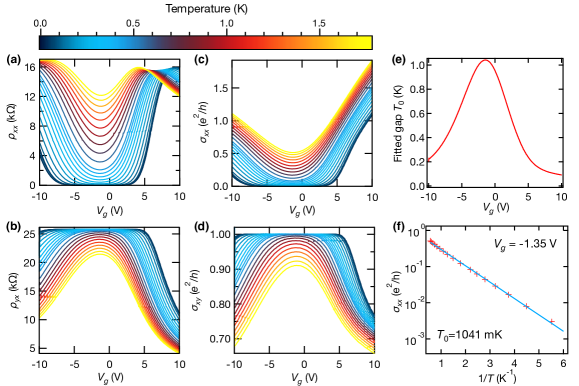
In an ideal QAH sample, zero longitudinal resistivity, , occurs simultaneously with quantized Hall resistivity, (note that in 2D ). Measurements of as a function of gate voltage and temperature are often used to determine when the electrostatic top gate has tuned the Fermi level to the center of the magnetic exchange gap, where the QAH state is most robust.
Empirically, we have observed that position of the native Fermi level in our Cr-BST films shifts over time, with optimal gate voltages moving towards more positive values. This observation holds true for the sample studied here where the optimal gate voltage appears to have shifted to be near V (described in Section S3.3 below) compared to the optimal gate voltage of V observed in different sample made from the same film two years earlier.
Two years prior to the measurements presented in the main text, a 100 m wide Hall bar was fabricated from the same 6-QL Cr-BST thin-film described in Section S3.1. This device was was characterized using standard lock-in amplifier techniques. A source current of nA RMS biased the Hall bar. Measurements of the longitudinal voltage and Hall (transverse) voltage were made as a function of top gate voltage and temperature . From these measurements, he longitudinal resistivity was calculated as:
| (S2) |
where is the transverse width of the Hall bar device and is the center-to-center distance between the voltage probes used to measure . The Hall resistivity was also calculated:
| (S3) |
along with the longitudinal conductivity:
| (S4) |
and the Hall conductivity:
| (S5) |
.
These measurements are shown in Fig. S4(a)–(d). At base temperature we observe a large plateau spanning V to V where , , and indicating that the Fermi level is positioned within the magnetic exchange gap. Beyond these gate voltages, increased dissipation and deviations from quantization become apparent as a the Femi level approaches the dissipative surface states. Within the plateau, dissipation appears thermally activated with above mK as seen in Fig. S4(d). The fitted thermal activation temperature scale peaks at V with mK as shown in Fig. S4(e).
S3.3 Measuring using the CCC’s nanovoltmeter
After the QAH device was cooled to base temperature, the device was magnetized by applying a 1 T field out of plane and then reducing the field to 0 T. The CCC’s NVM was used measure as was done in a previous work [S5]. A schematic depicting the longitudinal measurement configuration is shown in Fig. S5. It is important to note that Fig. S5 is only depicting the QAH device within the context of longitudinal resistivity measurements and does not include the PJVS or its associate electronics. The PJVS was present during these longitudinal measurements, and connected to the QAH device via the interposer (see Section S9) but was inactive (i.e. the microwave excitation was turned off and V).
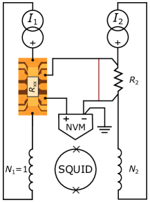
To measure , using the CCC’s NVM, the digital current source biased the QAH device. The second resistor network was shorted so the CCC’s NVM could be accessed independently and used to measure . The CCC’s compensation network and digital current source were both inactive. Measurements of were then used to compute the longitudinal resistivity via Eq. S2.
S3.4 Determining the optimal gate voltage of the QAH device
Measurements of as a function of top gate voltage were made with a fixed 100 nA bias current and are shown in Fig. S6. Measurements of made just after the device had been magnetized when the temperature at the sample stage was 9 mK, show a local minimum near V(red dots). Fig. S6 also shows measurements of made when the sample stage temperature was 8.8 mK (blue squares). This second set of measurements took place after the system was given several hours to equilibrate since being heated by ramping the superconducting magnet during the initial magnetization process.
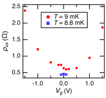
Given that the minimum value of was observed for top gate voltages very near 0 V, we concluded that the native Fermi level was well positioned near the center of the magnetic exchange gap. Therefore, all measurements were taken with zero volts applied to the top gate.
S4 QCS Measurements
S4.1 The CCC’s digital current source
As stated in the main text, the CCC’s digital current source acted as the bias source for the QAH device during QCS measurements and was also the current source to be measured by the QCS.
Importantly, the current source operates using a 16-bit digital-to-analog converter (DAC)[40]. Therefore could not be changed continuously but had to be incremented in pre-defined steps using a graphical user interface (GUI).
In the manuscript the source currents are referenced to 3 significant figures for simplicity. Additionally, and any currents that were within 500 AA of one another were grouped into a signal data point (using the arithmetic mean) for clarity. Table 2 below shows the 11 values of current measured in this work. The first column, , gives the value of sourced current as it was shown on the CCC’s GUI. The second column, , gives the step size to the next highest value on the GUI that was measured (if applicable for the manuscript). The third column gives the value that was used to reference the corresponding value of in the manuscript.
Generally it was found that the CCC’s GUI indicated a slightly larger value of nominal current than what was measured by either or . The largest disagreement between and or was roughly -300 AA for nA. As described in Section S2.2, in normal operation of the CCC it is ratio of and that matters, not the absolute value of either bias current. Accordingly these small deviations (on the order of tens or hundreds of AA) do not impact the overall function of the CCC. It is therefore unsurprising that these deviations have not been noticed during prior operation of the instrument.
| (nA) | (AA) | (nA) |
| 9.329500 | – | 9.33 |
| 27.97940 | 325.2 | 28.0 |
| 27.98850 | – | 28.0 |
| 53.78890 | – | 53.8 |
| 83.92895 | 109.0 | 83.9 |
| 83.93810 | 109.6 | 83.9 |
| 83.94730 | – | 83.9 |
| 132.3893 | 68.7 | 132 |
| 132.3984 | – | 132 |
| 251.8235 | 36.1 | 252 |
| 251.8326 | – | 252 |
S4.2 Corresponding values of , , and
Three frequencies were shown to have limited impact on quantization (see Section S5). These frequencies were GHz, GHz, and GHz. All data were acquired at one of these three frequencies, with the exception the variational measurements of Fig. 3.
The PJVS output voltage is given by:
| (S6) |
where is the number of active Josephson junctions (JJs) biased at frequency to be on their first Shapiro step, and is the Josephson constant. As discussed in the Methods section of the main text, individual JJs are grouped into subarrays on the PJVS and so can take corresponding values of 12, 36, 108, and 324. The constraints on and limited the possible values of accessible during QCS measurements. We emphasize that constraints on do not limit the accuracy or precision of QCS because the offset of from is measured directly as described in the main text. However, choosing to be as close as possible to allows one to make use of the benefits associate with making a null measurement as opposed to a full-scale measurement of the voltage. The values of , , used during QCS measurements of current are given in Table 3.
| (nA) | N | (mV) | |
| 9.33 | 12 | 0.2407232 | |
| 28.0 | 36 | 0.7221697 | |
| 53.8 | 36 | 1.388444 | |
| 83.9 | 108 | 2.166442 | |
| 132 | 108 | 3.416889 | |
| 252 | 324 | 6.499527 |
S4.3 Determination of and
Measurements of using the QCS ultimately amount to measurement of via Eq. (2) of the main text. Measurement of requires accurate measurement of . To eliminate thermoelectric offsets in the polarity of the input current was reversed periodically for a total of cycles. For all measurements . Fig. S7(a) shows an example measurement of plotted as a function of of the number of samples taken (red dots) taken when the bias current nA. For this particular measurement polarity cycles were preformed.
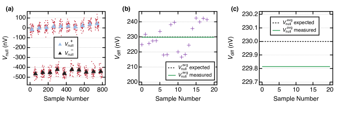
For the measurement shown in Fig. S7, current polarity reversal occurred every 60 seconds. After each reversal the system was given 10 seconds to equilibrate. was then sampled 40 times per polarity at a rate of one sample per second.
The overall value of used in Eq. (2) of the main text was determined using the following procedure. First, the average value of for each polarity of the cycles was calculated. Let () be the average value of for the positive (negative) portion of a polarity reversal cycle (shown a triangular markers in Fig. S7(a)). The difference between and for consecutive consecutive polarities was then calculated as:
| (S7) |
yielding a total of values for each with an independent standard deviation . These 2n-1 values of are again averaged using an inverse variance weighting to produce a final averaged value of . It is this final averaged value that is used to calculate via Eq. (2) of the main text.
Fig. S7(b) shows the 19 values of obtained using the data from Fig. S7(a). The final averaged value of these data points is shown as a solid green line (‘ measured’).
Also shown in Fig. S7(b) is the expected average value of (black dashed lined). This is the final averaged value of that one expects to measured based on the measurements of made using the indirect measurement scheme shown in Fig. 2(a) of the main text. Concretely, ‘ expected’ was determined by:
| (S8) |
S4.4 Comparison of , , and
As discussed in the main text, one current source was used for all measurements presented in this work. Table 4 below shows , the nominal sourced current as indicated by the CCC’s GUI. In the main text currents within one setting of another were grouped into an average value for ease of display. The individual values are given in Table 4 below.
| (nA) | (nA) | (nA) | (nA) |
| 9.3 | 9.329500 | 9.328131 | 9.328337 |
| 27.8 | 27.97940 | 27.97921 | 27.97988 |
| 27.8 | 27.98850 | 27.98659 | 27.98659 |
| 53.8 | 53.78890 | 53.78686 | 53.78732 |
| 83.9 | 83.92895 | 83.91331 | 83.91356 |
| 83.9 | 83.93810 | 83.92265 | 83.92263 |
| 83.9 | 83.94730 | 83.92946 | 83.92964 |
| 132.4 | 132.3893 | 132.3733 | 132.3750 |
| 132.4 | 132.3984 | 132.3832 | 132.3843 |
| 251.8 | 251.8235 | 251.7836 | 251.7877 |
| 251.8 | 251.8326 | 251.7938 | 251.7972 |
S5 Heating of the QAH device via microwave leakage
It is well documented that both the longitudinal and Hall resistivities of QAH devices are strongly dependent on temperature. This can be seen in Section S3.2 where at V increased by two orders of magnitude between mK and K while decreased by roughly 20%. The sensitivity of QAH properties to changes in either lattice or electron temperature must therefore be considered whenever these materials are used.
As noted in the main text, heating of the QAH device was observed due to leakage of the PJVS’s microwave bias. The measurements shown below were taken before those presented in the main text. Initially, the system was cooled without any shielding placed around the PJVS or the QAH device. It immediately became apparent that the QAH device was experiencing significant heating when the microwave bias to the PJVS was on. This can be seen in Fig. S8 by comparing measurements of taken with the microwave bias turned off (, blue triangles) and those taken with the microwave bias on when there was no radiative shielding present (red squares). At the lowest currents the longitudinal resistivity measured with the microwave on was approximately double that measured when it was off. At the highest currents the discrepancy rose to be roughly a factor of 20. The same measurements were performed after warming up the system and adding copper shielding around the PJVS, revealing a substantial reduction in dissipation compared to measurements without the shielding. We believe that the strong dependence on is related to excitation of the cavity modes of the dilution refrigerator.
In some cases, after changing several hours were needed for the system to come to equilibrium. This can be seen in Fig. S8(c) where, after changing by less than 1% from an initial frequency of , more than four hours were needed for the QAH device to equilibrate. Waiting for such long time scales was not feasible and therefore the frequency was fixed to one of the three for which heating was found to have minimal effects on (see Section S2.2).
Radiative leakage was also seen to affect the temperature reading of the ruthenium oxide resistance thermometer near the sample stage where the QAH device was located. Fig. S8(d) shows simultaneous measurements of and (where is the ruthenium oxide resistance thermometer’s temperature reading) as a function of time after the PJVS bias frequency was turned on ( GHz, 0 dBm).
S6 National Metrology Institutes Referenced for Calibration and Measurement Capability Data
The blue shaded region in Figure 2(b) of the main text shows the typical calibration precision ranges offered by the following national netrology institutes: Istituto Nazionale di Ricerca Metrologica (INRIM), Korea Research Institute of Standards and Science (KRISS), Van Swinden Laboratory (VSL), the Swiss Federal Institute of Metrology (METAS), the National Institute of Metrology, China (NIMC), VTT Technical Research Centre of Finland’s Centre for Metrology (VTT), Laboratoire national de métrologie et d’essais (LNE), Physikalisch-Technische Bundesanstalt (PTB), and Research Institutes of Sweden (RISE).
S7 Long Term Drift of the CCC’s Digital Current Source
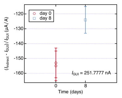
Fig. S9 shows evidence of drift in the output current of the CCC’s digital current source. The y-axis shows the deviation of the measured value of from the nominal value of the output current in units of AA. The x-axis shows the time (in days) each measurement was taken. The error bars represent the Type A statistical uncertainty of the measurements ().
Two measurements of were taken on day zero. Both of these measurements indicated that the the output current of the CCC was slightly lower in magnitude than the GUI indicated value but, within uncertainty, these measurements were equal to one another. Eight days later, the exact same measurement was repeated. Again the measurement indicated that the output current of the CCC was slightly lower than the GUI indicated value. However, the amount of deviation measured on day eight was not consistent with what was measured on day zero. Instead, the measurement on day eight indicated that the output current was slightly larger in magnitude than what is was on day zero. This drift could explain the discrepancy between some of the measurements of and as discussed in the main text.
S8 Uncertainty Budget and Noise Analysis
S8.1 Uncertainty budget for measurements of
This section provides additional details regarding the contributions to the total uncertainty budget for measurements of .
Type A contribution:
-
•
Null detector reading, : calculated as the standard deviation of means of multiple polarity reversals within a single experimental run. Lower values of current are naturally subject to larger amounts of relative dispersion given the lower signal to noise ratio and thus this contribution is largest for the lowest values of current.
Type B contributions:
-
•
NVM input impedance: When a digital voltmeter (DVM) is used to measure , or the null between and , a voltage divider is formed between source impedances—such as the QAH device itself and resistive filters in the wiring—and the input impedance of the DVM. The same is true of any leakage resistance in the wiring. The Keysight 3458A DVM used for the indirect measurements—in which only is measured—was experimentally determined to have an input impedance approaching 1 T. Thus, its contribution to the uncertainty of the indirect current measurements is less than 0.1 A/A. In a null measurement, the uncertainty contribution of the divider to the voltage estimate is diminished by the ratio of the null voltage to (or ). The Keithley 2182A NVM used for direct measurements of current was specified by its manufacturer to have an input impedance greater than 10 G. Assuming a worst-case null ratio of , the contribution of the NVM input impedance to the uncertainty would be less than 0.005 A/A.
-
•
NVM gain and linearity: Similar to above, for direct/null measurements, the contribution of the nanovoltmeter’s gain and nonlinearity to the overall uncertainty is diminished by the ratio of the null voltage to . Even so, the Keithley 2182A used in these measurements was calibrated using NIST’s conventional digital multimeter calibration service. For the 10 mV range, the gain error was 24 V/V and the nonlinearity was less than 4 V/V (note that minimum calibrated voltage was 1 mV). Assuming the same worst-case null ratio of , the contribution of the uncorrected NVM gain error and nonlinearity to the uncertainty would be less than 0.03 A/A.
-
•
PJVS microwave bias error: The laboratory where the DR was installed did not have access to a GPS-disciplined frequency standard. Instead, we used a commercial waveform generator (Keysight 33622A) with an onboard oven-controlled quartz crystal oscillator (OCXO) as our 10 MHz frequency reference. The RF bias for the PJVS was phase locked to this standard for all measurements. We checked the frequency of the OCXO reference against a GPS-disciplined standard in a separate laboratory prior to and after our measurement campaign. Its frequency offset at both times was nHz/Hz. We also checked for phase locked loop deficiencies within the RF generator by measurements against a high frequency counter. No issues were found. We did not correct for the frequency offset of our reference in the uncertainty budget because its contribution amounts to only 0.01 A/A
-
•
combined uncertainty: is measured using a CCC as a ratio measurement against a standard resistor. The following are the sources of uncertainty for this measurement.
-
–
Type A uncertainty related to the dispersion of the bridge voltage difference (BVD) measurements and its repeatability.
-
–
Type B uncertainty related to the SQUIDs rectification of noise causing an offset in the BVD measurement. This can be measured by measuring the BVD with the current sources off.
-
–
Compensation network drift: Type B uncertainty due to the drift of the compensation network. The compensation network is a series-parallel combination of resistors which act to bring the BVD as close to zero as possible. Typically this network is calibrated once a year.
-
–
Standard resistor: Combined uncertainty of the standard resistor used to characterize the QAH device. We used a calibrated 100 standard resistor as the reference for these measurements with an estimated uncertainty of 3 n (k = 1)
-
–
Leakage: We estimated electric isolation of the lines and connections to be on the order of 100 . This results in a relative error of a few and mostly limits the precision of the resistance measurements.
-
–
CCC winding ratio error: The windings of the CCC used in this work were set by connecting a series of windings with different turns in an arithmetic combination. For ratios other than 1:1, the errors must be determined by a step-up calibration procedure based on intercomparisons of all windings [S6,S7] This error is small and on the order of a few parts in but must be taken into account.
-
–
S8.2 Uncertainty budget for measurements of
The uncertainty budget for measurements of consisted of the Type A uncertainty of the DVM readings ranged from 0.60 AA at 252 nA to 31.0 AA at 9.33 nA. The budget also includes the relative Type B uncertainty of the DVM due to its finite input impedance, gain and non-linearity. The total Type B relative uncertainty of was estimated to be 1.01 AA.
S8.3 Allan deviation calculation
For time-series or time-domain measurements (like the measurements of sampled at a fixed interval ), the magnitude of the Allan deviation (referred to as in the main text), is inversely indicative of the stability of the measurement (i.e. a smaller magnitude indicates greater measurement stability). When plotted on a - scale, the functional dependence of on is commonly used to determine the type of noise that dominates a measurement over a given time scale [S8]. For example, the Allan deviation for white noise limited data will scale as whereas data dominated by noise will have an Allan deviation that appears constant as a function of .
NIST special publication 1065 by Riley et al. [S9] provides extensive details on stability analysis methods for time and frequency domain measurements. The stability and noise analysis protocols used in this work largely followed the guidance of that publication. Specifically, the time series data for was detrended by subtracting a linear function in time. This removes correlations caused by linear thermal drift [S9].
Next, the overlapping Allan variance was calculated using equations (11) from reference [S9]:
| (S9) |
Here is the sample of for , is the averaging factor, and is the general sampling interval. Use of the overlapping Allan variance is increase the confidence in stability estimates by utilizing all possible combinations of the data compared to the non-overlapping form [S9].
S9 The Interposer
To facilitate independent, in situ measurement of the QAH device, a custom interposer was placed between the PJVS and the QAH device at the 4 K stage micro-D connector. The interposer functioned as a straight-thru fnr cable, which was shunted with a 1 nF ceramic capacitor to reduce differential noise originating from the PJVS during direct mode measurements. When QAH quantization or indirect current measurements were performed, the capacitor was shunted by the superconducting state of the PJVS.
References
[S1] M. Gotz et al., IEEE Trans. Instrum. Meas., 2009, 58, 1176–1182.
[S2] D Drung et al., Supercond. Sci. Technol., 2009, 22, 114004.
[S3] D. Drung et al., IEEE Trans. Instrum. Meas., 2013, 62, 2820–2827.
[S4] E. J. Fox et al., Phys. Rev. B, 2018, 98, 075145.
[S5] L. K. Rodenbach et al., Phys. Rev. Appl., 2022, 18, 034008.
[S6] K. Grohmann et al., IEEE Trans. Instrum. Meas., 1979, 28, 205–211.
[S7] Y. Lu et al.,Method for the Calibration of Cryogenic Current Comparator Ratios 2020 Conference on Precision
Electromagnetic Measurements (CPEM), 2020, pp. 1–2.
[S8] D. W. Allan, IEEE Trans. Instrum. Meas., 1987, 646–654.
[S9] W. J. Riley et al., Handbook of frequency stability analysis, US Department of Commerce, National Institute of
Standards and Technology, 2008.