Epitaxial Kagome Thin Films as a Platform for Topological Flat Bands
Abstract
Systems with flat bands are ideal for studying strongly correlated electronic states and related phenomena. Among them, kagome-structured metals such as CoSn have been recognized as promising candidates due to the proximity between the flat bands and the Fermi level. A key next step will be to realize epitaxial kagome thin films with flat bands to enable tuning of the flat bands across the Fermi level via electrostatic gating or strain. Here we report the band structures of epitaxial CoSn thin films grown directly on insulating substrates. Flat bands are observed using synchrotron-based angle-resolved photoemission spectroscopy (ARPES). The band structure is consistent with density functional theory (DFT) calculations, and the transport properties are quantitatively explained by the band structure and semiclassical transport theory. Our work paves the way to realize flat band-induced phenomena through fine-tuning of flat bands in kagome materials.
keywords:
kagome material, angle-resolved photoemission spectroscopy, flat band, molecular beam epitaxyStrongly correlated electronic systems are one of the focuses of condensed matter physics due to the emergence of interesting many-body ground states. Materials with dispersionless bands, i.e. flat bands, are ideal systems for studying the physics of strongly correlated electronic states due to the smaller bandwidth as compared to the Coulomb repulsion . One noted example is the flat band in twisted bilayer graphene, which is responsible for various correlated phenomena such as tunable superconductivity 1, 2, magnetism 3 and metal-to-insulator transitions 4. Another important class of materials exhibiting flat bands are those composed of quasi-two-dimensional (2D) kagome lattices. Examples in this family include CoSn 5, 6, Fe3Sn2 7, Co3Sn2S2 8, YMn6Sn6 9 and Ni3In 10. In 2D kagome lattices, the flat band emerges due to the destructive phase interference of the electronic wave functions within the hexagons of the kagome lattice. This mechanism generates electronic states confined within these hexagons in real space and appears as non-dispersing bands in momentum space 11, 5, 6. Theoretically, a 2D kagome lattice generates a perfect flat band in the tight-binding model considering only nearest-neighbor hopping. In real materials, the actual band structure can deviate from the ideal case due to the existence of additional hopping terms and spin-orbit coupling 5.
For realizing flat-band-induced phenomena in kagome metals, it is important to fine-tune the flat band position relative to the Fermi level since many physical properties are dominated by states at the Fermi level. To this end, synthesizing epitaxial thin films of kagome metals provides several strategies for tuning the flat bands. The highly-controlled growth process using molecular beam epitaxy (MBE) allows one to chemically dope the material, while after the growth, device patterning and voltage gating is another way to tune the flat bands. In addition, anisotropic strains can be applied to thin films through either epitaxial growth or mechanical methods. All these potential advantages provide strong motivation for investigating flat-band-hosting kagome thin films. While tunneling spectroscopy has provided indirect evidence for the existence of flat bands in epitaxial FeSn films 12, direct observation of flat bands in kagome thin films has been missing.
In terms of material selection, CoSn stands out due to the existence of flat bands several hundreds of meV below Fermi level and spread across a large portion of the Brillouin zone (BZ) 13. In CoSn bulk crystals, such flat bands have been confirmed by angle-resolved photoemission spectroscopy (ARPES) experiments 5, 6, 14. Recent work further established the connection between flat bands in CoSn and the observed large resistance within the kagome plane as compared to perpendicular to the kagome plane 14. Regarding the thin film growth, there has been one work reporting epitaxial CoSn thin films on metallic buffer layers by magnetron sputtering 15. Although the previously reported sputtered CoSn thin films showed physical properties that are consistent with the bulk crystals, the direct evidence of flat bands in CoSn thin films remains elusive 15. Furthermore, a challenge for epitaxial kagome films is the difficulty of growing continuous films directly onto insulating substrates, 16 which are favored for voltage gating and transport studies.
In this paper, we demonstrate epitaxial CoSn thin films grown on insulating substrates as a promising platform to realize flat-band physics. The growth of (0001)-oriented CoSn thin films on insulating MgO(111) and 4H-SiC(0001) substrates was enabled by a three-step MBE growth recipe. Using synchrotron-based ARPES, we directly measured the band structure of the CoSn thin films, and revealed multiple flat bands. At the point, spin-orbit coupling (SOC) gaps were observed between one of the flat bands and the quadratic bands, suggesting the nontrivial topology of this flat band. Using density functional theory (DFT) calculations, we studied the tunability of the flat bands through carrier doping and found that the calculations are consistent with the ARPES experiments. Finally, we measured the transport properties of CoSn and quantitatively explained the results using the band structure and semiclassical transport theory.
The CoSn thin films were grown on MgO(111) or 4H-SiC(0001) substrates by MBE using a three-step recipe. First, a 5 nm seed layer was deposited at 500 ∘C (470 ∘C) on 4H-SiC(0001) (MgO(111)) substrates, followed by a 1520 nm continuation layer grown at 100 ∘C. The third step is the growth of a terminating layer of 510 nm CoSn at 300 ∘C. Details of the growth (and other methods) are provided in the Supporting Information (SI) section S1.
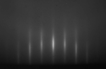
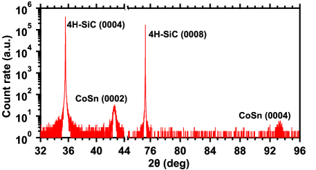
Figure LABEL:fig:RHEED shows the in-situ reflection high-energy electron diffraction (RHEED) pattern of a 35 nm CoSn thin film grown on 4H-SiC(0001) substrate. The streaky RHEED pattern indicates epitaxial growth and two-dimensional surfaces with finite terrace width. The X-ray diffraction (XRD) data of a 35 nm CoSn thin film grown on 4H-SiC(0001) substrate is shown in Figure LABEL:fig:XRD (the RHEED and XRD data of CoSn films grown on MgO(111) substrates are provided in the SI section S2). Besides the substrate peaks at 32.57 ∘ and 75.34 ∘, two additional peaks show up at 42.57 ∘ and 93.34 ∘, corresponding to CoSn (0002) and (0004) peaks, respectively. The out-of-plane lattice constant extracted from the XRD scan is 4.254 Å, which is in good agreement with the previous studies on bulk crystals 17 and sputtered thin films 15.
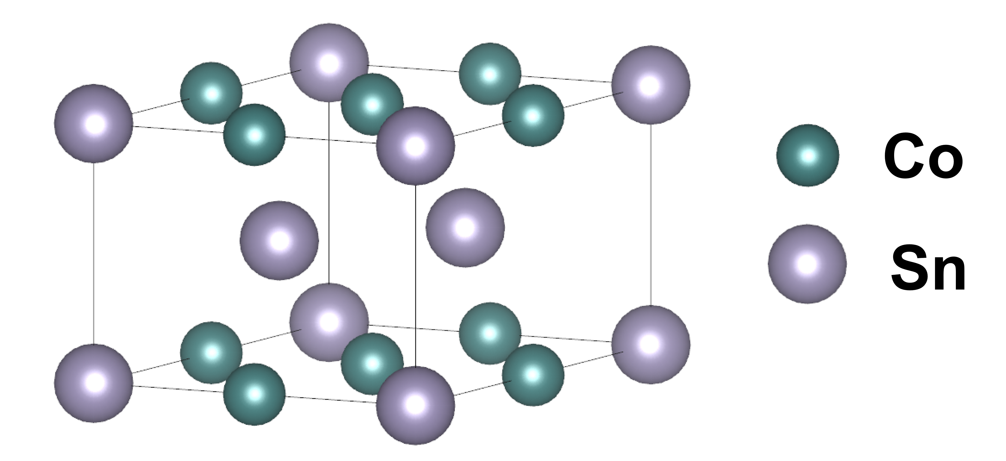
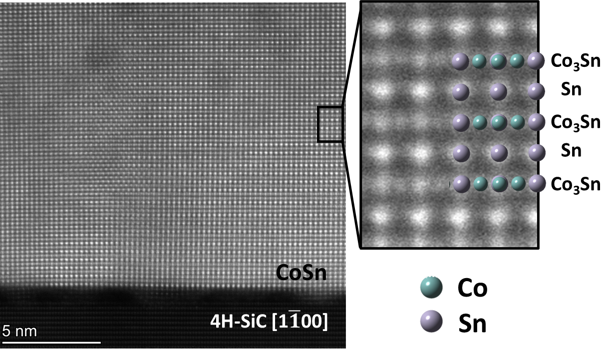
High-angle annular dark-field (HAADF) scanning transmission electron microscopy (STEM) imaging was performed to examine the crystalline characteristics of the CoSn thin film (see SI section S1.2 for methods). Figure LABEL:fig:TEM shows an atomic-resolution HAADF-STEM image of a 35 nm CoSn(0001) thin film on 4H-SiC(0001) viewed along 4H-SiC[100] axis. The HAADF-STEM image reveals the alternating stacking sequence of one Co3Sn kagome layer and one Sn2 honeycomb layer, which is expected for CoSn (see Figure LABEL:fig:structure). The brightness of atomic columns in the HAADF-STEM image is approximately proportional to the square of the atomic number (Z), consequently, Sn (Z=50) atom columns appear as brighter columns while a mixture of CoSn atom columns and Co (Z=27) atom columns appear dimmer. Although the sequence of the alternating stacking of one Co3Sn layer and one Sn2 layer is predominant across the film, in some regions closer to the interface, the sequence is alerted by the addition of extra Co3Sn layers (See SI section S3).
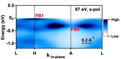
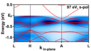
Having synthesized the epitaxial CoSn thin films, the questions one would raise is whether or not our thin films have flat bands, and whether or not the flat bands are topologically nontrivial if they exist. The most straightforward method to answer these questions is to directly measure the band structures using ARPES. In this study, we utilized the synchrotron-based ARPES to map the band structures of a 25 nm CoSn thin films grown on MgO(111) and 4H-SiC(0001) substrates (see SI section S1.3 for methods). In the following discussion, we will mainly focus on the band structures of CoSn on 4H-SiC(0001) substrates, while the band structures of CoSn on MgO(111) substrate are presented in SI section S4.1. Figure LABEL:fig:FB_97eVLH shows the band structures measured using s-polarized (s-pol) photons with 97 eV energy, which corresponds to (mod ) plane in the momentum space (see SI section S4.2 for kz dependence of ARPES spectrum, and SI section S4.3 for ARPES spectra taken with p-polarized light). In this plane, two dispersionless bands can be observed - one band centers around the H point (labeled as “FB1” in Figure LABEL:fig:FB_97eVLH) close to the Fermi level, while the other band (“FB2”) resides deeper below the Fermi level and spreads over almost the entire BZ. Lorentzian fitting of energy distribution curves (EDCs) around the H point gives a binding energy of -0.04 eV for FB1, with effective mass =16.7 along the H-L direction, where is the mass of free electrons. Meanwhile, fitting EDCs at the A and L points yields -0.31 eV and -0.32 eV binding energies, respectively (see SI section S4.4 for details).
It is noteworthy that FB1 is reported to be accountable for the anomalous anisotropic transport properties and orbital magnetic moment in bulk CoSn, due to its proximity to the Fermi level14. Another work demonstrates that tuning FB1 to the Fermi level through chemical doping induces antiferromagnetic ordering at low temperatures18. In our work, FB1 lies just below the Fermi level at the H points, which is promising for tuning it across the Fermi level in the near future.
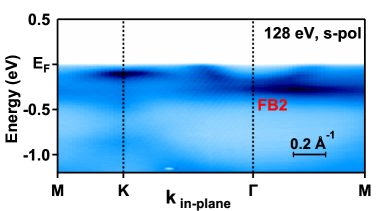
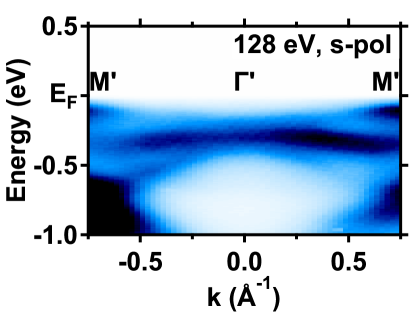
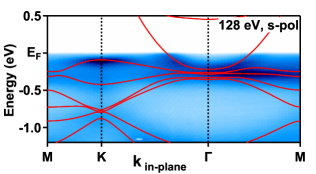
We next measured the band structures of CoSn thin films in the (mod ) plane by changing the photon energy to 128 eV. Different from the (mod ) plane in which two sets of flat bands can be observed, in the (mod ) plane only the FB2 can be seen 0.3 eV below the Fermi level. The fitting results of the EDCs at multiple high-symmetry points across the 1st BZ suggest that the variation of FB2 binding energy is within 0.03 eV, signifying the dispersionless nature of FB2 (See SI section S4.4).
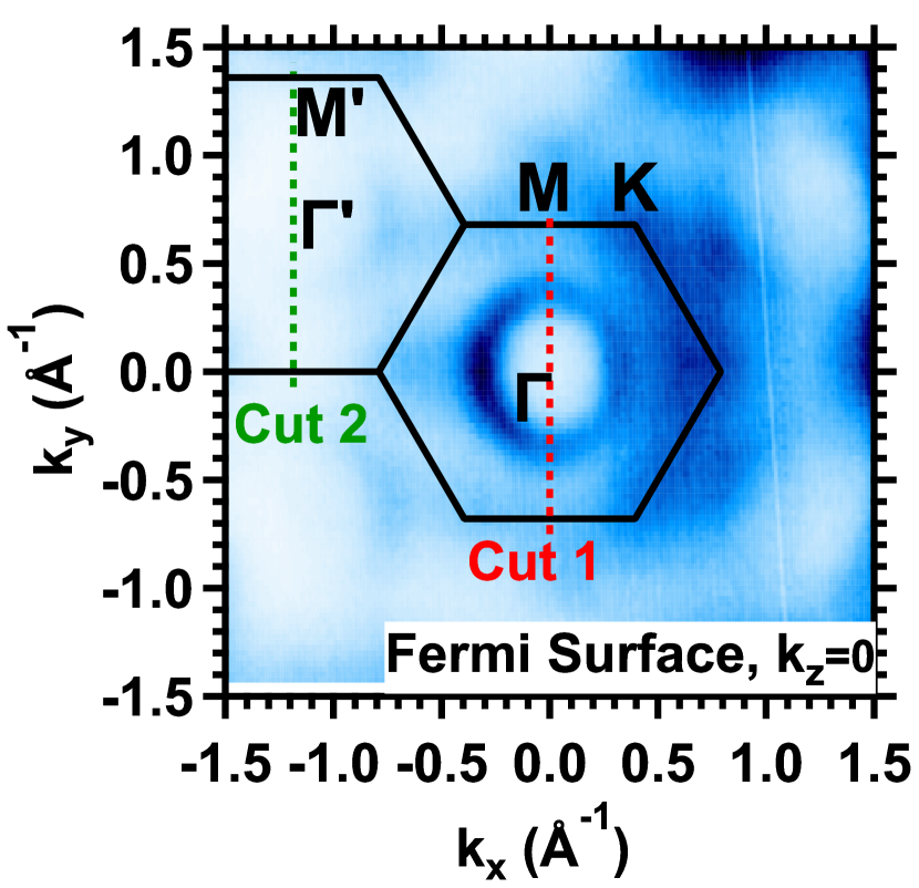
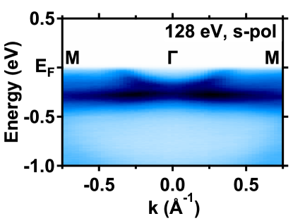
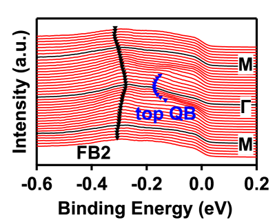
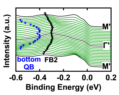
An important question yet to be answered is whether the flat bands are topologically non-trivial for the CoSn thin films. Theoretically, the spin-orbit coupling (SOC) opens a gap between the flat band and quadratic band (QB) at the band touching point, making the flat band topologically non-trivial 19, 20, 21. To verify this, we analyzed the spectrum around the point, where FB2 touches the QB. The spectrum along the M--M direction (“Cut 1” in Figure LABEL:fig:FermiSurface_128eVLH) in the 1st BZ clearly captures FB2 and the top QB, as shown in Figure LABEL:fig:MGM_1stBZ. Lorentzian fitting of representative EDCs along this direction yields a SOC gap of 0.12 eV between FB2 and the top QB (Figure LABEL:fig:EDC_Stack_MGM). Meanwhile, the spectrum intensity of the bottom QB is maximized in the 2nd BZ along M’-’-M’ direction (“Cut 2” in Figure LABEL:fig:FermiSurface_128eVLH), as shown in Figure LABEL:fig:MGM_2ndBZ. A similar analysis yields a 0.09 eV SOC gap between FB2 and the bottom QB (see Figure LABEL:fig:EDC_Stack_MG1M). Compared to the reported 0.04 to 0.08 eV SOC gap reported in CoSn bulk crystals 5, 6, the SOC gap for the thin film is slightly larger.
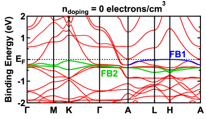
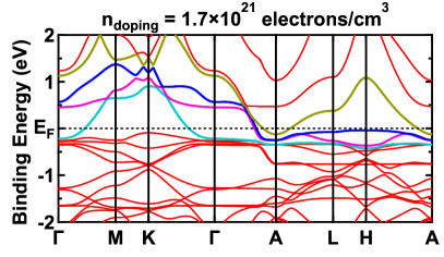
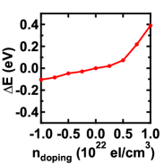
To investigate the tunability of the flat bands by carrier doping, we performed density functional theory (DFT) calculations (see SI section S1.4 for methods). Figure LABEL:fig:DFT_prisrtine shows the band structure of pristine CoSn without carrier doping. This calculation suggests that FB1 sits exactly at the Fermi level at the H point, while FB2 has a binding energy of -0.26 eV at the point. We performed additional DFT calculations with different doping concentrations ranging from 1.01022 holes/cm3 to 1.01022 electrons/cm3 (see SI section S5). Within this doping range, adding electrons to the system () shifts the FB1 downwards with respect to the Fermi level, while the band dispersion only changes slightly. The energy shift of FB1 at the H point as a function of doping level is summarized in Figure LABEL:fig:DFT_energy_shift. We calculated the band structure with arbitrary doping level by linearly interpolating the DFT results. Matching the binding energies of FB1 at the H point and FB2 at the point yields a doping level of 1.71021 electrons/cm3 and a binding energy renormalization factor of 0.85 (see Figure LABEL:fig:DFT_doped). An overlay of DFT bands on top of the ARPES spectra shows a good agreement between them, as shown in Figure LABEL:fig:DFT_stack_97eVLH and LABEL:fig:DFT_stack_128eVLH.
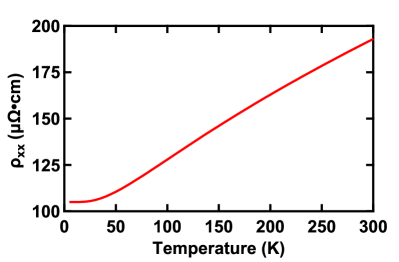
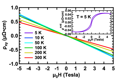
Figure LABEL:fig:Rxx shows the longitudinal resistivity of a 35 nm CoSn thin film grown on MgO(111) substrate as a function of temperature (see SI section 1.5 for methods). At room temperature, the CoSn thin film has a resistivity of 192 cm. As the temperature decreases from room temperature, the resistivity drops almost linearly down to 30 K, then reaches a plateau of 105 cm. The Hall resistivity of the same sample at different temperatures is shown in Figure LABEL:fig:Hall. At room temperature, the Hall resistivity shows linear behavior with respect to the magnetic field, with no detectable anomalous Hall effect. This observation is in agreement with the non-magnetic nature of CoSn 22. However, as the temperature drops below 10 K, an anomalous Hall effect starts to appear, although the amplitude is no larger than 0.05 cm (See inset of Figure LABEL:fig:Hall). This tiny anomalous Hall effect was also observed in sputtered thin films 15 and similar signals were observed in low-temperature magnetization measurements of bulk crystals 6. The mechanism behind it is suggested to be either a small deviation in stoichiometry or magnetism induced by the flat band 15. The extracted carrier density is 6.57 electrons/cm3 at room temperature and 3.91 electrons/cm3 at 5 K, respectively.
The relationship between the transport properties and the band structure of CoSn has been discussed qualitatively 5, 6, 14, however, a quantitative discussion has been missing. Meanwhile it is important to quantitatively understand the relationship between the transport properties and the band structure of CoSn, especially to disentangle the contribution from individual bands, since the transport measurements provide indirect evidence for flat bands near the Fermi level 17, 14. Here we provide an estimate of Hall resistivity from DFT-calculated band structures. In semiclassical transport theory, the contribution to longitudinal conductivity from band is given by 23:
| (1) |
where is the carrier relaxation time, is the energy dispersion, and is the distribution function. Meanwhile, the contribution to Hall conductivity from band is given by 23:
| (2) |
Since only partially occupied bands contribute to the transport at low temperatures, we hereby calculated the and for the bands crossing the Fermi level, namely band I (cyan), II (pink), III (blue), and IV (gold) in Figure LABEL:fig:DFT_doped (see SI section S6 for details). Assuming a universal and k-independent relaxation time for all bands, we calculated the Hall coefficient by 23:
| (3) |
which is independent of relaxation time . With this method, our theory gives a Hall resistivity of -1.010-9 m3/C, which has the same order of magnitude as the experimental value of -1.610-9 m3/C at T = 5 K. The major contribution to the Hall coefficient comes from band I (see Table S2 in the SI), which has a large electron pocket around the point. This analysis also yields values for that are consistent with our experimental results if we assume reasonable values for , as discussed in SI section S6. Our theoretical modeling bridges the gap between the band structure and the experimentally measured transport properties of CoSn.
In conclusion, we synthesized the epitaxial CoSn thin films directly on insulating substrates and studied their electronic band structures. The three-step growth generated highly ordered CoSn (0001) thin films, as confirmed by a combination of RHEED, XRD, and STEM. The electronic band structures of CoSn thin films were measured with synchrotron-based ARPES. The flat bands were clearly visualized and the topologically non-trivial nature of the flat band is signified by the spin-orbit coupling gap at the band touching point. The ARPES measurement, DFT calculations, and the transport properties of CoSn are consistent with each other not only qualitatively but also quantitatively. One very interesting direction in the near future will be the fabrication of devices that allows voltage gating in order to tune the flat bands across the Fermi level. This work makes the epitaxial CoSn thin films ready for studies of strongly correlated electronic states and flat band-induced phenomena.
Methods
See SI section S1.
Methods (MBE, STEM, ARPES, DFT, transport measurements), RHEED and XRD of CoSn on MgO(111), additional STEM data, additional ARPES data, additional DFT calculations, and estimation of longitudinal conductivity and Hall conductivity.
We thank Dr. Tiancong Zhu for technical assistance. This work was supported by NSF Grant No. 1935885, AFOSR MURI 2D MAGIC Grant No. FA9550-19-1-0390, U.S. DOE Office of Science, Basic Energy Sciences Grants No. DE-SC0016379 and No. DE-SC0004890, the Center for Emergent Materials, an NSF MRSEC, under Grant No. DMR-2011876, and the UB Center for Computational Research. This research used resources of the Advanced Light Source, which is a DOE Office of Science User Facility under contract No. DE-AC02-05CH11231. Electron microscopy was performed at the Center for Electron Microscopy and Analysis (CEMAS) at The Ohio State University.
Author Contributions Statement
S.C., M.N., W.Z., A.J.B., C.J., A.B., and E.R. performed ARPES measurements. S.C. and R.K.K. analyzed the ARPES data. S.C. performed MBE growth, transport measurements, and theoretical modeling of transport data. T.Z. and I.Ž performed DFT calculations. N.B. and D.W.M. performed STEM measurements. I.L. performed XRD measurements and fabricated devices. S.C. and R.K.K. conceived the project and R.K.K. supervised the project. All authors contributed to writing the manuscript.
References
- Cao et al. 2018 Cao, Y.; Fatemi, V.; Fang, S.; Watanabe, K.; Taniguchi, T.; Kaxiras, E.; Jarillo-Herrero, P. Unconventional superconductivity in magic-angle graphene superlattices. Nature 2018, 556, 43–50
- Yankowitz et al. 2019 Yankowitz, M.; Chen, S.; Polshyn, H.; Zhang, Y.; Watanabe, K.; Taniguchi, T.; Graf, D.; Young, A. F.; Dean, C. R. Tuning superconductivity in twisted bilayer graphene. Science 2019, 363, 1059–1064
- Wolf et al. 2019 Wolf, T. M.; Lado, J. L.; Blatter, G.; Zilberberg, O. Electrically tunable flat bands and magnetism in twisted bilayer graphene. Physical Review Letters 2019, 123, 096802
- Lu et al. 2019 Lu, X.; Stepanov, P.; Yang, W.; Xie, M.; Aamir, M. A.; Das, I.; Urgell, C.; Watanabe, K.; Taniguchi, T.; Zhang, G.; Bachtold, A.; MacDonald, A. H.; Efetov, D. K. Superconductors, orbital magnets and correlated states in magic-angle bilayer graphene. Nature 2019, 574, 653–657
- Kang et al. 2020 Kang, M.; Fang, S.; Ye, L.; Po, H. C.; Denlinger, J.; Jozwiak, C.; Bostwick, A.; Rotenberg, E.; Kaxiras, E.; Checkelsky, J. G.; Comin, R. Topological flat bands in frustrated kagome lattice CoSn. Nature Communications 2020, 11, 4004
- Liu et al. 2020 Liu, Z.; Li, M.; Wang, Q.; Wang, G.; Wen, C.; Jiang, K.; Lu, X.; Yan, S.; Huang, Y.; Shen, D.; Yin, J.-X.; Wang, Z.; Yin, Z.; Lei, H.; Wang, S. Orbital-selective Dirac fermions and extremely flat bands in frustrated kagome-lattice metal CoSn. Nature Communications 2020, 11, 4002
- Lin et al. 2018 Lin, Z. et al. Flatbands and emergent ferromagnetic ordering in Fe3Sn2 kagome lattices. Physical Review Letters 2018, 121, 096401
- Yin et al. 2019 Yin, J.-X. et al. Negative flat band magnetism in a spin–orbit-coupled correlated kagome magnet. Nature Physics 2019, 15, 443–448
- Li et al. 2021 Li, M.; Wang, Q.; Wang, G.; Yuan, Z.; Song, W.; Lou, R.; Liu, Z.; Huang, Y.; Liu, Z.; Lei, H.; Yin, Z.; Wang, S. Dirac cone, flat band and saddle point in kagome magnet YMn6Sn6. Nature Communications 2021, 12, 3129
- Ye et al. 2021 Ye, L.; Fang, S.; Kang, M. G.; Kaufmann, J.; Lee, Y.; Denlinger, J.; Jozwiak, C.; Bostwick, A.; Rotenberg, E.; Kaxiras, E.; Bell, D. C.; Janson, O.; Comin, R.; Checkelsky, J. G. A flat band-induced correlated kagome metal. arXiv [cond-mat.mtrl-sci] 2021, 2106.10824, https://doi.org/10.48550/arXiv.2106.10824, (accessed 2023-07-19)
- Li et al. 2018 Li, Z.; Zhuang, J.; Wang, L.; Feng, H.; Gao, Q.; Xu, X.; Hao, W.; Wang, X.; Zhang, C.; Wu, K.; Dou, S. X.; Hu, Z.; Du, Y. Realization of flat band with possible nontrivial topology in electronic Kagome lattice. Science Advances 2018, 4, eaau4511
- Han et al. 2021 Han, M.; Inoue, H.; Fang, S.; John, C.; Ye, L.; Chan, M. K.; Graf, D.; Suzuki, T.; Ghimire, M. P.; Cho, W. J., et al. Evidence of two-dimensional flat band at the surface of antiferromagnetic kagome metal FeSn. Nature Communications 2021, 12, 5345
- Meier et al. 2020 Meier, W. R.; Du, M.-H.; Okamoto, S.; Mohanta, N.; May, A. F.; McGuire, M. A.; Bridges, C. A.; Samolyuk, G. D.; Sales, B. C. Flat bands in the CoSn-type compounds. Physical Review B 2020, 102, 075148
- Huang et al. 2022 Huang, H.; Zheng, L.; Lin, Z.; Guo, X.; Wang, S.; Zhang, S.; Zhang, C.; Sun, Z.; Wang, Z.; Weng, H.; Li, L.; Wu, T.; Chen, X.; Zeng, C. Flat-Band-Induced Anomalous Anisotropic Charge Transport and Orbital Magnetism in Kagome Metal CoSn. Physical Review Letters 2022, 128, 096601
- Thapaliya et al. 2021 Thapaliya, T.; Yoo, T.; Hurtado Parra, S.; Arndt, N. D.; Need, R.; Kikkawa, J. M.; Kim, H.; Huang, S. High-quality epitaxial thin films of topological kagome metal CoSn by magnetron sputtering. Applied Physics Letters 2021, 119, 201902
- Hong et al. 2022 Hong, D.; Liu, C.; Wen, J.; Du, Q.; Fisher, B.; Jiang, J.; Pearson, J. E.; Bhattacharya, A. Synthesis of antiferromagnetic Weyl semimetal Mn3Ge on insulating substrates by electron beam assisted molecular beam epitaxy. APL Materials 2022, 10, 101113
- Sales et al. 2021 Sales, B.; Meier, W.; May, A.; Xing, J.; Yan, J.-Q.; Gao, S.; Liu, Y.; Stone, M.; Christianson, A.; Zhang, Q.; McGuire, M. A. Tuning the flat bands of the kagome metal CoSn with Fe, In, or Ni doping. Physical Review Materials 2021, 5, 044202
- Sales et al. 2022 Sales, B. C.; Meier, W. R.; Parker, D. S.; Yin, L.; Yan, J.; May, A. F.; Calder, S.; Aczel, A. A.; Zhang, Q.; Li, H., et al. Chemical Control of Magnetism in the Kagome Metal CoSn1-xInx: Magnetic Order from Nonmagnetic Substitutions. Chemistry of Materials 2022, 34, 7069–7077
- Sun et al. 2011 Sun, K.; Gu, Z.; Katsura, H.; Sarma, S. D. Nearly flatbands with nontrivial topology. Physical Review Letters 2011, 106, 236803
- Guo and Franz 2009 Guo, H.-M.; Franz, M. Topological insulator on the kagome lattice. Physical Review B 2009, 80, 113102
- Bolens and Nagaosa 2019 Bolens, A.; Nagaosa, N. Topological states on the breathing kagome lattice. Physical Review B 2019, 99, 165141
- Allred et al. 2012 Allred, J.; Jia, S.; Bremholm, M.; Chan, B.; Cava, R. Ordered CoSn-type ternary phases in Co3Sn3-xGex. Journal of Alloys and Compounds 2012, 539, 137–143
- Hurd 1972 Hurd, C. M. Hall effect in metals and alloys; Plenum Press, New York, 1972; p 72
TOC Graphic
![[Uncaptioned image]](/html/2307.15828/assets/x17.png)