Analog programming of CMOS-compatible Al2O3/TiO memristor at after metal-insulator transition suppression by cryogenic reforming
Abstract
The exploration of memristors’ behavior at cryogenic temperatures has become crucial due to the growing interest in quantum computing and cryogenic electronics. In this context, our study focuses on the characterization at cryogenic temperatures () of TiO-based memristors fabricated with a CMOS-compatible etch-back process. We demonstrate a so-called cryogenic reforming (CR) technique performed at to overcome the well-known metal-insulator transition (MIT) which limits the analog behavior of memristors at low temperatures. This cryogenic reforming process was found to be reproducible and led to a durable suppression of the MIT. This process allowed to reduce by approximately 20% the voltages required to perform DC resistive switching at . Additionally, conduction mechanism studies of memristors before and after cryogenic reforming from to revealed different behaviors above , indicating a potential change in the conductive filament stoichiometry. The reformed devices exhibit a conductance level that is 50 times higher than ambient-formed memristor, and the conduction drop between and is 100 times smaller, indicating the effectiveness of the reforming process. More importantly, CR enables analog programming at with typical read voltages. Suppressing the MIT improved the analog switching dynamics of the memristor leading to approximately 250% larger on/off ratios during long-term depression (LTD)/long-term potentiation (LTP) resistance tuning. This enhancement opens up the possibility of using TiO-based memristors to be used as synapses in neuromorphic computing at cryogenic temperatures.
Memristors are among the leading candidates for the large-scale integration of non-volatile memory and artificial synapses in neuromorphic architectures Li et al. (2018). While their characteristics have been widely investigated at , the growing interest in quantum computing and cryogenic electronics has led to new concepts based on memristors to overcome some of the engineering challenges encountered in scaling-up quantum computers Vandersypen et al. (2017). Recent works propose developing cryogenic-compatible CMOS-memristor hybrid circuits for applications such as tunable cryogenic DC sources Mouny et al. (2023), the charge state autotuning of quantum dots Czischek et al. (2021), quantum error correction Marcotte et al. (2023) or spiking neural networks Chen et al. (2021). In this context, cryogenic studies have been conducted on various types of emerging memory based on HfO2Voronkovskii et al. (2019); Fang et al. (2015); Hao et al. (2021); Blonkowski and Cabout (2015), AlO Huang et al. (2020), NiO Alagoz et al. (2023), TaO Zhang et al. (2014), TiO Pickett et al. (2011); Beilliard et al. (2020) and ferroelectric HZO Manchon et al. (2022); Chen et al. (2023). Among these candidates, TiO based memristors present the most promising characteristics at room temperature including fully analog behaviour, low switching voltages and CMOS-compatibility Kim et al. (2021). However, the cryogenic DC characterizations of memristors based on TiO exhibit a metal-insulator transition (MIT) at low voltages below Beilliard et al. (2020); Pickett et al. (2011); Alagoz, Chow, and Jung (2019). This MIT is attributed to the Ti4O7 Magnéli phase and hinders its usage at cryogenic temperatures by limiting its ohmic region.
In this work, we report a specific reforming methodology at cryogenic temperatures aiming to suppress the MIT of Al2O3/TiO memristors. We investigate the impact of both ambient temperature forming (AF) and cryogenic reforming (CR) on the conduction mechanisms of our devices from to . Finally, we demonstrate that the suppression of the MIT allows the quasi-linear analog tuning of the memristor resistance at using voltage pulses in a long-term depression (LTD)/long-term potentiation (LTP) tuning scheme.
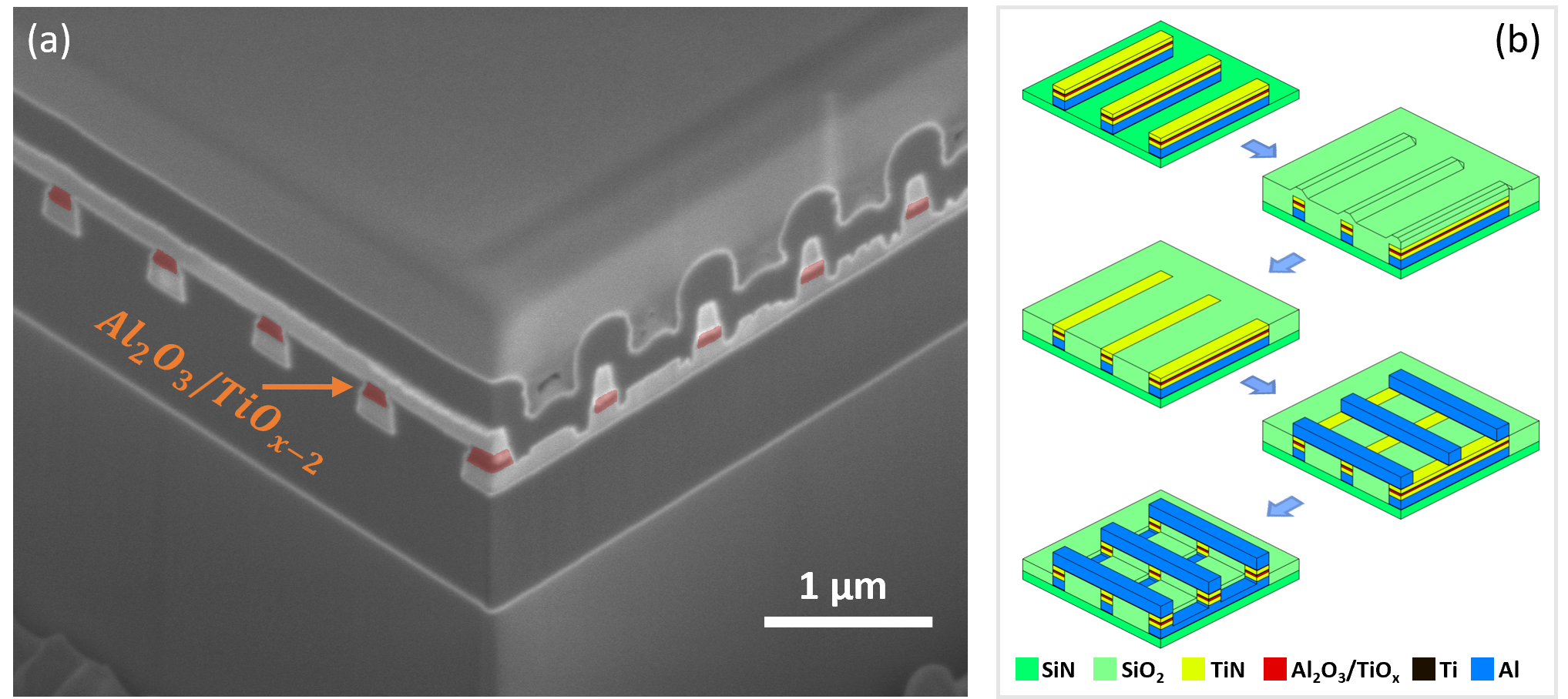
The devices investigated consist of Ti/Al/TiN - Al2O/TiO/Ti - TiN/Ti/Al, which represent the bottom electrode (BE), active stack and top electrode (TE), respectively. The process flow is illustrated in Fig. 1(b). The first step of fabrication involves the sputtering deposition of a Ti ()/Al ()/TiN () stack for the BE. This is followed by the deposition of the active switching stack of Al2O3 () through atomic layer deposition, and TiO () by reactive sputtering, along with Ti ()/TiN (). The vacuum was not broken between the depositions of the TiO, Ti and TiN layers. A -wide BE is patterned using electron beam lithography (EBPG5200), a negative resist (MaN2405) and an inductively coupled plasma (ICP) etching process with BCl3/Cl2/Ar chemistry. The BEs and the switching stack are both encapsulated through the deposition of of SiO2 using plasma-enhanced chemical vapor deposition (PECVD). Subsequently, a chemical-mechanical polishing (CMP) process is applied to planarize the SiO2 surface and reveal the top surface of the BE. The TiN layer serves as a polishing stop layer for the CMP process. The SiO2 dishing between the BE, measured by atomic force microscopy (AFM), is less than . A -wide TE made of Ti ()/Al () is deposited and patterned similarly to the BE. The active stack between the TE lines is removed during the etching step of the TE. The devices are then encapsulated with a layer of SiO2 deposited by PECVD. Vias to contact the electrodes are patterned using electron beam lithography and ICP etching with SF6 chemistry. Finally, Al () connection lines are patterned to address the memristors. After this, a 1-minute rapid thermal annealing step at under an N2 atmosphere is performed. As shown in the focused ion beam (FIB) isometric cross-section in Fig. 1(a), the memory stack lies only at the intersection of the BEs and TEs, like a similar approach presented in the literature Dawant, Ecoffey, and Drouin (2022).
The memristor crosspoints are characterized from to with a Keysight B1500A semiconductor device parameter analyzer with a waveform generator module (WGFMU) on a Lakeshore CPX-VF cryogenic probe station. Both the sample and the magnet stage are heated when the device is warmed up to ensure temperature stability. For all measurements, the BEs are grounded and the signals are applied to the TEs. The memristor resistances are measured at low bias () with a DC sweep for the conduction mechanism studies, and they are measured with a / read pulse during pulsed characterizations. For all DC measurements, we limited the maximum current through the memristor to using a custom current compliance board placed at to avoid overshoot during forming and DC sweeps. Prior to the cooldown, 10 memristors are ambient-formed (AF) at . We perform I-V measurements to benchmark the non-volatile switching of our devices at room temperature (see Fig. 1(c)). The sample is then cooled down to .
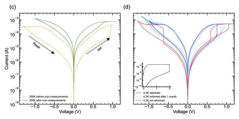
The first I-V measurements at on an AF memristor exhibit the MIT introduced by the Ti4O7 Magnéli phase, as depicted by the red curve in Fig. 1(d) Pickett et al. (2011); Beilliard et al. (2020). By applying an approximately two-times-larger positive DC sweep with a compliance current to an AF memristor, one can observe an abrupt increase of the measured current up to the compliance current at , as shown in the inset of Fig. 1(d). This phenomenon is similar to electroforming and suggests that the conductive filament of the memristor is reformed. After this CR, we observe that consecutive DC switchings do not exhibit the characteristic MIT anymore as shown by the blue curve in Fig. 1(d). The CR process is reproducible as we create five reformed devices with similar DC behavior. Moreover, the DC cycle at after the cooldown exhibits a lower low resistance state (LRS) and high resistance state (HRS) compared to before CR was performed, suggesting that the diameter of the conductive filament is larger due to CR as observed in Fig. 1(c). These CR memristor DC cycles show butterfly-shaped switchings as the room-temperature I-V curves measured prior to the cooldown. However, one can note that lower and were needed to switch the memristor at which is an interesting feature for low-power applications. We also investigate the retention of the MIT suppression by cooling down and measuring the same CR device one month later. The I-V characteristics of the CR memristor remained without MIT at (see the cyan curve in Fig. 1(d)). It suggests that a permanent change to the conductive filament was made through CR yielding to different conduction mechanisms at cryogenic temperatures.
To investigate the change in the conduction mechanisms involved in the MIT suppression, we perform additional DC cycle measurements for both AF and CR devices from to and extract the conductances at each temperature for the LRS by reading the current at . As shown in Fig. 2(c), the conductance decreases with temperature for the two types of devices. For the TiO memristors exhibiting the MIT (AF memristors), the temperature-dependant conductance can be described by an Arrhenius equation:
| (1) |
where depends on the transport mechanism (e.g., for nearest neighbor hopping (NNH) conduction Mott and Davis (2012)), is a pre-exponential factor and is the thermal activation energy Mott and Davis (2012); Beilliard et al. (2020). The LRS conductance of the AF memristor fits linearly with (1) for between and and between and which corresponds to Efros–Shklovskii variable-range hopping (ES-VRH) as reported in Ref.Beilliard et al. (2020).
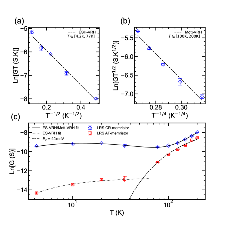
Regarding the CR devices, Fig. 2(b) shows a linear relationship between and from to . This indicates that the conduction in the oxide layer is governed by Mott’s variable-range-hopping (Mott-VRH) mechanism instead of the simple thermally activated hopping exhibited by the AF memristors. The conductance governed by the Mott-VRH law is given by
| (2) |
where is a characteristic temperature coefficient and is the conductance at Mott and Davis (2012); Yildiz et al. (2008). Meanwhile at lower temperatures, fits linearly with which suggests that the conduction mechanism is described by the ES-VRH law below (see Fig. 2(a)). The ES-VRH governed conductance is given by
| (3) |
Thus, the total conductance of the CR memristor can be defined using the sum of the contributions from the Mott-VRH conduction mechanism and the ES-VRH conduction mechanism Yildiz et al. (2008):
| (4) |
The total conductance predicted by Eq. 4 is in good agreement with our experimental data using the fitted parameters for the ES-VRH and Mott-VRH conduction mechanisms (see Fig. 2(c) for the fit and Table 1 for the fitted parameters).
The conduction mechanisms for differ for the CR (Mott-VRH) and AF (NNH) memristors which could explain the MIT suppression. The CR memristor exhibits conductances that are two orders of magnitude larger for temperature below the MIT temperature (100-) Pickett et al. (2011). The conductance of the AF memristor decreases by over two orders of magnitude from to while it decreases by only a factor of 5 for the CR memristor over the same temperature range. This validates the suppression of the MIT regime for the CR devices, as it does not exhibit an important conductance drop with decreasing temperature. The CR device shows a crossover from to dependence within the temperature range from to as demonstrated in Ref.Yildiz et al. (2008) for TiO2 thin films. This significant change in the conduction mechanisms governing the memristor conductance with respect to the temperature suggests that Ti4O7 has been suppressed. One possible explanation is that the previously crystalline conductive filament became amorphous due to a quenching effect during the reforming procedure at cryogenic temperatures, similarly to the switching mechanism of phase-change memory Gallo and Sebastian (2020), leading to the creation of an amorphous phase inside the conductive filament. This phase change of the oxide layer is validated by the retention of the reformed state demonstrated in Fig. 1(d), which suggests a durable suppression of Ti4O7 in the vicinity of the conductive filament.
| Fit | () | () | () |
|---|---|---|---|
| ES-VRH (no MIT) | 54.49 | N.A. | |
| Mott-VRH (no MIT) | 42.15 | N.A. | |
| NNH Arrhenius (MIT) | N.A. | 41.8 | |
| ES-VRH (MIT) | 46.1 | N.A. |
Finally, we investigate the impact of the MIT suppression induced by cryogenic reforming on the analog switching dynamics of our Al2O3/TiO memristors using pulse programming. To do this, we measure the same device before and after reforming. Resistance tuning is assessed on this memristor by measuring long-term resistance potentiation (LTP) and depression (LTD) at . A write/verify pulse train comprised of one / write pulse and one / (or ) read pulse is applied 50 times with a constant positive amplitude for the write pulse (LTP) and 50 times with a constant negative amplitude (LTD). This pattern is repeated seven times to verify the stability of the LTD/LTP tuning. This whole protocol is performed 10 times in order to evaluate the cycle-to-cycle variability (background shadow in Fig. 3).For the typical read voltage (), the resistance of the AF memristor remains unchanged, as the reading is performed in the insulator region of the memristor as depicted in Fig. 1(d). By increasing the reading voltage to to operate above the insulator regime, one can observe typical LTD/LTP resistance tuning for the AF memristor which exhibits an on/off ratio of for a write amplitude of . After reforming we repeat the measurement with the same write amplitude but lowered the read voltage to . In this case, the CR memristor demonstrates a larger on/off ratio of in a larger absolute memory window.
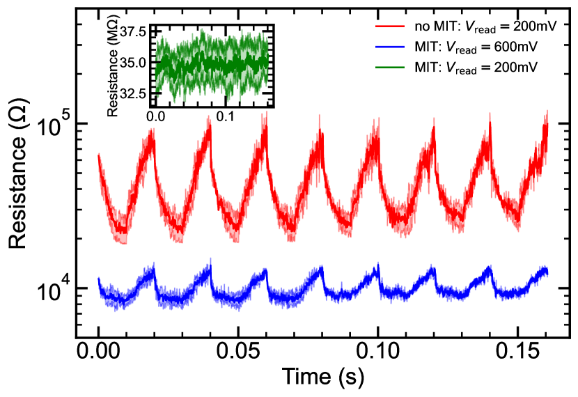
The LTP and LTD characteristics are quasi-linear and stable for both the AF memristor read at and CR memristor read at which ensures fully analog tunability of the memristor resistance over the respective to and to ranges before and after the reforming. Thus, reforming the memristors increases the resistance on/off ratio, which allows a larger resistance tunability in cryogenic neuromorphic circuit and an increased resolution for synaptic weight encoding. Additionally, one can observe that the reading region for CR memristors at (0-) is similar to the one exhibited at room temperature (see Fig. 1(c)). Having a large read region is an important feature for vector matrix multiplication (VMM) Li et al. (2017), as it improves the achievable resolution for the input vector and thus provides a more accurate VMM result overall Yao et al. (2020).
On the other hand, it was observed that AF memristors offered a smaller read region, ranging from to , along with smaller resistance values when the AF memristor is read in this region. Both the smaller resistance and the higher read voltage range introduce additional power consumption during inference which is detrimental in the context of cryogenic environments. However in the insulator region, the conductance of the AF memristor is not changed i.e., for amplitudes lower than . This property can be leveraged and used as a selector Beilliard et al. (2020). It would allow one to accurately program each device in a crossbar without influencing the resistance of the surrounding memristors Yan et al. (2016). This presents an interesting trade-off between the programming accuracy of the weights, the power consumption and the on/off resistance ratios. For applications that do not require to reprogram the crossbar several times, such as neural network inference accelerators Czischek et al. (2021), the CR approach should be preferred by taking advantage of the larger on/off ratios. For programming-intensive applications, the AF approach should be considered as the MIT induced selector could allow to program accurately large crossbars.
In conclusion, we conducted electrical characterizations of Al2O3/TiO2-x memristors at cryogenic temperatures and proposed a method called cryogenic reforming to suppress the metal-insulator transition introduced by Ti4O7 below . Using the cryogenic reforming methodology, we demonstrated resistive switching at without insulator regime and a retention of the MIT suppression for over a month hinting at a permanent change of the conductive filament. Moreover, the study of temperature dependence of the conductance suggests different conduction mechanisms for the AF and CR memristors from to . This validates the idea that the conductive filament has undergone intrinsic changes through the reforming process. The CR memristor exhibits a conduction drop at that is 100 times smaller than that of the AF memristor due to the MIT suppression. Finally, we demonstrated that CR memristors have a fully analog behavior at which would enable the development of memristor-based cryogenic electronics applied to quantum technologies. AF devices exhibit a smaller memory window but have a built-in selector below thanks to the MIT that could be utilized for large crossbar applications. Our work is a stepping stone towards memristor-based cryogenic applications in quantum technologies showing the viability of the TiO-based memristor at deep cryogenic temperatures.
This work was supported by the Natural Sciences and Engineering Research Council of Canada (NSERC) and the Canada First Research Excellence Fund (APOGEE). This research was undertaken thanks to support from Laboratoire Nanotechnologies Nanosystèmes (LN2), which is a French–Canadian Joint International Research Laboratory (IRL3463), funded and co-operated by Centre National de la Recherche Scientifique (CNRS), Université de Sherbrooke, Université de Grenoble Alpes (UGA), École Centrale Lyon (ECL), and Institut National des Sciences Appliquées (INSA) Lyon. We acknowledge financial support from the Fonds de Recherche du Québec Nature et Technologie (FRQNT).
AUTHOR DECLARATIONS
Conflicts of InterestThe authors have no conflicts to disclose.Author ContributionsPierre-Antoine Mouny: Conceptualization (equal); Data curation (equal); Formal analysis (lead); Investigation (lead); Methodology (lead); Validation (equal); Visualization (lead); Writing – original draft (lead); Writing – review & editing (equal). Raphaël Dawant: Conceptualization (equal); Data curation (supporting); Investigation (supporting); Resources (lead); Validation (equal); Visualization (supporting); Writing – original draft (supporting); Writing – review & editing (equal). Bastien Galaup: Data curation (equal); Formal analysis (supporting); Investigation (supporting); Methodology (supporting); Validation (equal); Writing – review & editing (equal). Serge Ecoffey: Project administration (supporting); Resources (supporting); Supervision (supporting); Validation (equal); Writing – review & editing (equal) Michel Pioro-Ladrière: Project administration (supporting); Funding Acquisition (supporting); Supervision (supporting); Writing – review & editing (equal). Yann Beilliard: Conceptualization (equal); Project administration (lead); Investigation (supporting); Supervision (supporting); Validation (equal); Writing – original draft (supporting); Writing – review & editing (equal) and Dominique Drouin: Conceptualization (equal); Funding acquisition (lead); Project administration (supporting); Supervision (lead); Validation (equal); Writing – original draft (supporting); Writing – review & editing (equal)DATA AVAILABILITYThe data underlying the results presented in this paper are not publicly available at this time but may be obtained from the authors upon reasonable request.
REFERENCES
References
- Li et al. (2018) Y. Li, Z. Wang, R. Midya, Q. Xia, and J. J. Yang, “Review of memristor devices in neuromorphic computing: Materials sciences and device challenges,” Journal of Physics D: Applied Physics 51, 503002 (2018).
- Vandersypen et al. (2017) L. M. K. Vandersypen, H. Bluhm, J. S. Clarke, A. S. Dzurak, R. Ishihara, A. Morello, D. J. Reilly, L. R. Schreiber, and M. Veldhorst, “Interfacing spin qubits in quantum dots and donors—Hot, dense, and coherent,” Quantum Information 3 (2017), 10.1038/s41534-017-0038-y.
- Mouny et al. (2023) P.-A. Mouny, Y. Beilliard, S. Graveline, M.-A. Roux, A. E. Mesoudy, R. Dawant, P. Gliech, S. Ecoffey, F. Alibart, M. Pioro-Ladrière, and D. Drouin, “Memristor-based cryogenic programmable DC sources for scalable in situ quantum-dot control,” IEEE Transactions on Electron Devices 70, 1989–1995 (2023).
- Czischek et al. (2021) S. Czischek, V. Yon, M.-A. Genest, M.-A. Roux, S. Rochette, J. C. Lemyre, M. Moras, M. Pioro-Ladrière, D. Drouin, Y. Beilliard, and R. G. Melko, “Miniaturizing neural networks for charge state autotuning in quantum dots,” Machine Learning: Science and Technology 3, 015001 (2021).
- Marcotte et al. (2023) F. Marcotte, P.-A. Mouny, V. Yon, G. A. Dagnew, B. Kulchytskyy, S. Rochette, Y. Beilliard, D. Drouin, and P. Ronagh, “A cryogenic memristive neural decoder for fault-tolerant quantum error correction,” (2023), arXiv:2307.09463 [quant-ph] .
- Chen et al. (2021) A. Chen, Z. Zhang, G. Ma, N. Liu, C.-Y. Lin, W.-C. Chen, T.-C. Chang, and H. Wang, “Comprehensive regulation of the threshold oscillation for neuromorphic systems based on cryogenic performance of NbO2 device,” IEEE Electron Device Letters 42, 692–695 (2021).
- Voronkovskii et al. (2019) V. A. Voronkovskii, V. S. Aliev, A. K. Gerasimova, and D. R. Islamov, “Conduction mechanisms of TaN/HfOx/Ni memristors,” Materials Research Express 6, 076411 (2019).
- Fang et al. (2015) R. Fang, W. Chen, L. Gao, W. Yu, and S. Yu, “Low-temperature characteristics of HfOx-based resistive random access memory,” IEEE Electron Device Letters 36, 567–569 (2015).
- Hao et al. (2021) Z. Hao, B. Gao, M. Xu, Q. Hu, W. Zhang, X. Li, F. Sun, J. Tang, H. Qian, and H. Wu, “Cryogenic HfOx-based resistive memory with a thermal enhancement capping layer,” IEEE Electron Device Letters 42, 1276–1279 (2021).
- Blonkowski and Cabout (2015) S. Blonkowski and T. Cabout, “Bipolar resistive switching from liquid helium to room temperature,” Journal of Physics D: Applied Physics 48, 345101 (2015).
- Huang et al. (2020) X.-D. Huang, Y. Li, H.-Y. Li, K.-H. Xue, X. Wang, and X.-S. Miao, “Forming-free, fast, uniform, and high endurance resistive switching from cryogenic to high temperatures in W/AlOx/Al2O3/Pt bilayer memristor,” IEEE Electron Device Letters 41, 549–552 (2020).
- Alagoz et al. (2023) H. S. Alagoz, M. Egilmez, J. Jung, and K. H. Chow, “The influence of thermal cycling on the activation energy of conduction electrons and filament temperature in Pt/NiOx/Pt ReRAMs,” Applied Physics Letters 122 (2023), 10.1063/5.0151967.
- Zhang et al. (2014) Y. Zhang, N. Deng, H. Wu, Z. Yu, J. Zhang, and H. Qian, “Metallic to hopping conduction transition in Ta2O5-x/TaOy resistive switching device,” Applied Physics Letters 105, 063508 (2014).
- Pickett et al. (2011) M. D. Pickett, J. Borghetti, J. J. Yang, G. Medeiros-Ribeiro, and R. S. Williams, “Coexistence of memristance and negative differential resistance in a nanoscale metal-oxide-metal system,” Advanced Materials 23, 1730–1733 (2011).
- Beilliard et al. (2020) Y. Beilliard, F. Paquette, F. Brousseau, S. Ecoffey, F. Alibart, and D. Drouin, “Investigation of resistive switching and transport mechanisms of Al2O3/TiO2-x memristors under cryogenic conditions (1.5 K),” AIP Advances 10, 025305 (2020).
- Manchon et al. (2022) B. Manchon, D. Coffineau, G. Segantini, N. Baboux, P. Rojo Romeo, R. Barhoumi, I. Cañero Infante, F. Alibart, B. Vilquin, D. Drouin, et al., “Study of polarisation and conduction mechanisms in ferroelectric Hf0. 5Zr0. 5O2 down to deep cryogenic temperature 4.2 K,” (2022).
- Chen et al. (2023) Y.-C. Chen, Y.-C. Chen, K.-Y. Hsiang, M.-H. Lee, and P. Su, “Performance evaluation of aferam under low temperature operation,” in 2023 7th IEEE Electron Devices Technology & Manufacturing Conference (EDTM) (2023) pp. 1–3.
- Kim et al. (2021) H. Kim, M. R. Mahmoodi, H. Nili, and D. B. Strukov, “4K-memristor analog-grade passive crossbar circuit,” Nature Communications 12 (2021), 10.1038/s41467-021-25455-0.
- Alagoz, Chow, and Jung (2019) H. S. Alagoz, K. H. Chow, and J. Jung, “Low-temperature coexistence of memory and threshold switchings in Pt/TiOx/Pt crossbar arrays,” Applied Physics Letters 114, 163502 (2019).
- Dawant, Ecoffey, and Drouin (2022) R. Dawant, S. Ecoffey, and D. Drouin, “Multiple material stack grayscale patterning using electron-beam lithography and a single plasma etching step,” Journal of Vacuum Science & Technology B 40, 062603 (2022), https://pubs.aip.org/avs/jvb/article-pdf/doi/10.1116/6.0002116/16571016/062603_1_online.pdf .
- Mott and Davis (2012) N. F. Mott and E. A. Davis, Electronic processes in non-crystalline materials (Oxford University Press, 2012).
- Yildiz et al. (2008) A. Yildiz, S. Lisesivdin, M. Kasap, and D. Mardare, “Electrical properties of TiO2 thin films,” Journal of Non-Crystalline Solids 354, 4944–4947 (2008).
- Gallo and Sebastian (2020) M. L. Gallo and A. Sebastian, “An overview of phase-change memory device physics,” Journal of Physics D: Applied Physics 53, 213002 (2020).
- Li et al. (2017) C. Li, M. Hu, Y. Li, H. Jiang, N. Ge, E. Montgomery, J. Zhang, W. Song, N. Dávila, C. E. Graves, Z. Li, J. P. Strachan, P. Lin, Z. Wang, M. Barnell, Q. Wu, R. S. Williams, J. J. Yang, and Q. Xia, “Analogue signal and image processing with large memristor crossbars,” Nature Electronics 1, 52–59 (2017).
- Yao et al. (2020) P. Yao, H. Wu, B. Gao, J. Tang, Q. Zhang, W. Zhang, J. J. Yang, and H. Qian, “Fully hardware-implemented memristor convolutional neural network,” Nature 577, 641–646 (2020).
- Yan et al. (2016) B. Yan, A. M. Mahmoud, J. J. Yang, Q. Wu, Y. Chen, and H. H. Li, “A neuromorphic asic design using one-selector-one-memristor crossbar,” in 2016 IEEE International Symposium on Circuits and Systems (ISCAS) (2016) pp. 1390–1393.