Raman spectroscopy of monolayer to bulk PtSe2 exfoliated crystals
Abstract
Raman spectroscopy is widely used to assess the quality of 2D materials thin films. This report focuses on , a noble transition metal dichalcogenide which has the remarkable property to transit from a semi-conductor to a semi-metal with increasing layer number. While polycrystalline can be grown with various crystalline qualities, getting insight into the monocrystalline intrinsic properties remains challenging. We report on the study of exfoliated 1 to 10 layers by Raman spectroscopy, featuring record linewidth. The clear Raman signatures allow layer-thickness identification and provides a reference metrics to assess crystal quality of grown films.
Transition Metal Dichalcogenides (TMDs) are promising materials for future electronic and optoelectronic devices, owing to their large optical absorption per layer and high electronic mobility [1, 2]. Furthermore, they feature strong van der Waals interlayer coupling, resulting in a tunable layer-dependent band structure. Among TMDs, thin films of Platinum Diselenide () are semi-conductors and feature exceptional bandgap variations, with a transition to a semi-metal with increasing thickness [1, 3, 4, 5]. For this reason it can reach small bandgap values, permitting efficient photodetection in the infrared range [1, 3, 6]. This makes a promising building block for optoelectronic devices operating in the telecom band, and several growth methods (CVD, TAC, MBE) are being developed to provide high-quality scalable films for industry [3, 7, 8, 9, 10, 11, 2, 12]. These films are commonly characterized using a variety of methods, including electron diffraction, X-ray spectroscopy or diffraction, electron microscopy, atomic force microscopy, electronic transport measurements and optical spectroscopy [13, 2].
Among these methods, Raman spectroscopy presents several key advantages: fast, cheap and non-contact, it probes optical phonon transitions – highly sensitive to defects – and is therefore used as a primary characterization to identify the structure and assess film quality [14, 15, 16, 17, 18]. Previous works on established the most salient Raman spectral features [19, 20, 21, 22, 23, 24, 25]: they identified the optical vibrational phonon modes associated with the peaks, detailed the Raman peaks intensities and shifts evolution with the thickness, proposed quality metrics, and studied the polarization and temperature dependencies of the Raman peaks. However, due to the limited quality of the studied samples, the precise features of the Raman signature of few-layer intrinsic remained out of reach.
In this work, we report high-resolution Raman spectroscopy of record-quality exfoliated crystals of layer-controlled thickness. We establish criteria for film quality, and demonstrate that the characteristic Raman signature of thin flakes enables the determination of layer count. By providing reference Raman spectra of exfoliated single crystals, this work will guide the development of the continuously improving growth technology [8, 2, 12].
Samples Fabrication
Chemical Vapour Transport grown crystals (HQ Graphene [26]) are exfoliated on fused silica substrates, as shown in figure 1a. Au-assisted mechanical exfoliation provides flakes as thin as a monolayer thanks to the strong affinity of gold with Selenium atoms [27, 28, 29].
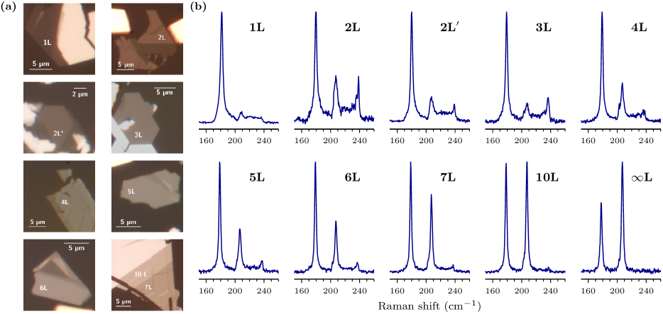
Each flake number of layers is identified using absorption microspectroscopy and confirmed by Atomic Force Microscopy, as described in detail in reference [12].
Atomic structure signature
High-resolution Raman spectroscopy is performed using a low-power green laser source, together with a edgepass filter (additional details in experimental section).
Spectra of selected flakes are displayed in figure 1b and consist in 3 solitary peaks in the spectral range. The flake thickness has little influence on the total scattered Raman intensity. This can be understood by the fact that green light is resonantly absorbed regardless of the number of layers [12]. The full set of spectra is included in the Supplementary Material (SM), figure LABEL:fig:ramanSpectraFull.
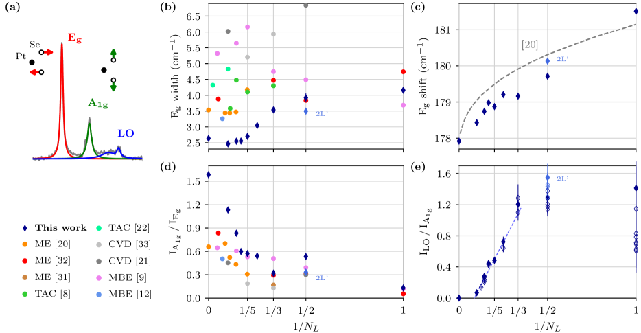
The spectral shapes correspond to the 1T phase of , identified with its 4 optical phonon modes: the Raman-active and modes around and respectively, and the IR-active and modes gathered as (longitudinal optical) around [19, 5, 30], as depicted in figure 2a.
Raman modes spectral weights and widths are assessed by a 4-components Lorentzian fit. Each Lorenzian function is parameterized by its shift , its integrated intensity , and full width at half maximum (thereafter abbreviated as width) , such that:
| (1) |
Selected fit parameters are gathered in figures 2b-e. More extensive data can be found in figure SMLABEL:fig:ramanFullParameters. Furthermore, the Raman signatures are mostly uniform over the flakes surfaces (down to the measurement accuracy, SMLABEL:fig:ramanMaps).
Almost all samples are identified using optical absorption spectroscopy as the most-stable AA stacking, as their optical absorption spectra match Density Functional Theory (DFT) predictions [12]. 2L’ samples are a noticeable exception, with a singular Raman signature differing from the one of 2L (detailed comparison in SMLABEL:fig:ramanBilayers). In fact, the comparison of absorption behavior with DFT predictions for 2L’ suggests an AB stacking [12], which has been theoretically identified as a stable phase for [30, 5, 34, 12], and is a common defect in grown films [35, 36].
The influence of the substrate on the Raman signature is moreover investigated. We compare the Raman spectra of few-layers flakes deposited on fused silica and crystalline sapphire (figure SMLABEL:fig:ramanSapphire). No noticeable difference can be observed, the Raman signature appearing to be identical. It is likely due to the fact that in both cases, the flakes and the substrate are not directly in van der Waals contact, due to the presence of interfacial layers of water [37].
Crystalline Quality
In TMDs and graphene, Raman mode linewidth is very sensitive to the defect level [14, 15, 16, 17]. is no exception, and the linewidth has been shown to increase with film defectiveness [22, 20, 8]. For the 1L flakes studied in this work, a narrow peak is associated with the presence of sharp optical features in the absorption spectrum [12], again indicating the relevance of this Raman spectral signature.
Recent works reported the growth of good quality films, using several methods: Thermally Assisted Conversion (TAC) [8, 22], Chemical Vapor Deposition (CVD) [33, 21] and Molecular Beam Epitaxy (MBE) [9, 12]. Some research focused instead on Mechanichally Exfoliated (ME) crystals [20, 31, 32]. These works stand out for their narrow peaks (figure 2b), with linewidths values below – reaching about for thick ME, TAC and MBE samples, about for ME and MBE 1L and 2L samples (however the film continuity of the MBE 1L is not established).
In our work, the high quality of the flakes is assessed by the unprecedented narrow linewidth of this mode, from monolayer to bulk thicknesses. The linewidth reaches for , for and around for thick samples ( to bulk). Among the exfoliated flakes studied, several feature large linewidths (), as shown in figure SMLABEL:fig:ramanFullParameters. We could not identify if such flakes were damaged during the exfoliation process, or if they originated from more defective areas of the original CVT crystal. As reported by the aforementioned works, the peak features of strong increase of its linewidth with decreasing film thickness (figure 2b). This increase is commonly attributed to increasing defectiveness as the film thickness diminishes [19].
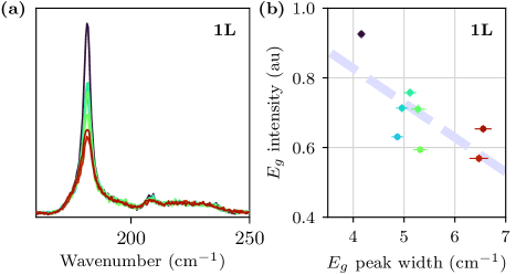
Let us now turn our examination from the peak width to its absolute intensity, which appears as a good criterion for film quality. Indeed, for a given layer count, the thin exfoliated flakes feature a large sample-to-sample variability of their peak integrated intensities (figure 3a for the 1L case), while the and modes are unaffected. We observe that higher peak intensity correlates with narrower linewidth (figure 3b, more thicknesses are studied in figure SMLABEL:fig:EgWidthInt), therefore appearing as a robust metric for film quality. This sensitivity of the mode intensity to flake quality may be due to the high sensitivity to the electromagnetic environment and disorder of Fröhlich electron-phonon coupling which affects longitudinal optical modes amplitudes in polar crystals [38, 39].
Number of Layers Identification
It is tempting to identify the number of layers from Raman signatures, in particular in in which the strong thickness-dependence Raman spectra led several authors to propose metrics relying on the shift of the peak or the ratio of to peak intensity. In this section, we show that these methods are imprecise, and we propose a new method for exfoliated crystals.
The peak position exhibits a quasi-linear blueshift with the inverse number of layers . The observed dependency in figure 2c is qualitatively compatible with previous studies, compiled as a grey dashed line and proposed as a metric by reference [20]. However, the discrepancy between this metrics and our data is too large to allow layer count identification.
The to peaks intensities is commonly considered as characteristic of the layer count [40, 20, 41]. Indeed the mode involves out-of-plane motion of external atoms (figure 2a) and its intensity rises with the thickness, while longitudinal optical modes disappear for high layer number [19]. These trends are observed as well in our work (figure 1b), but appear to be more complex for 1L and 2L. Nonetheless, the to intensities ratio does not appear as a reliable signature of the layer count, as it differs significantly from one research to another (figure 2d, references therein). Moreover, as described above, we observe for low layer count important variations of the peak intensity resulting in dispersion.
We propose instead to identify the number of layers by using the and peaks which are more robust to the defect level. The to intensity ratio for each sample is represented in figure 2e, as a function of inverse number of layers . One can see straight away that the thickness can be evaluated from to layers using the linear law displayed in figure 2e:
| (2) |
Mono- and bi-layers are exceptions to this law, but can be easily identified. Both present similar and peaks intensities, and 1L has a remarkably low to peaks intensities ratio, with with a singularly wide peak, while 2L has relatively high ratio , and a sharper peak (figure SMLABEL:fig:ramanFullParameters).
Beyond layers, accurate determination of the layer count isn’t critical anymore as AFM can provide a fair estimate.
Conclusion
By using exfoliated CVT crystals with layer-defined thickness, this study provides reference Raman spectrographs of high-quality flakes, which are particularly important for benchmarking emerging high-quality growth methods. We showed that crystalline quality can be assessed from the width and height of the mode peak, with linewidth narrowing down to for monolayer and for thicker exfoliated . We observed that commonplace criteria for layer count identification, either based on peak shift or on to peaks intensities ratio, leaves much to be desired for exfoliated high-quality . This led us to propose a robust method in this latter case based on the and specific peaks pattern.
Experimental Methods
Samples
A gold film is deposited using evaporation on a fused silica substrate (QX/QS Quartz Suprasil 300 from Hellma Analytics), on which the crystals are pre-exfoliated. The samples are then annealed at and the gold film is peeled using thermal release tape, thereby detaching few-layer . The peeled gold film is then transferred to a target substrate, and the gold is removed using etching.
Raman spectrometry
We use a Raman Qontor spectrometer from Renishaw with a grating, a microscope objective, a laser source and a edgepass filter. The laser is operated at a power of , in order to suppress any thermal shift or broadening of the lines (the spectral shift of the main peak was evaluated to reach approximately ). Each spectrum is integrated for and averaged 5 times. Muon peaks are eliminated from the spectra and the baseline is removed using a 3rd order polynomial fit of the background signal. The spectrometer is calibrated using a crystal which possesses a Raman peak centered at [42].
Acknowledgements
The authors acknowledge the financial support from the European Union’s Horizon 2020 program under grant agreement no. 785219, no. 881603 (Core2 and 3 Graphene Flagship), as well as from ANR-2018-CE08-018-05 (BIRDS) and ANR-2021-CE24-0025 (ELuSeM).
Data availability
The data that support the findings of this study are openly available, at [43].
References
- Zhao et al. [2017] Y. Zhao, J. Qiao, Z. Yu, P. Yu, K. Xu, S. P. Lau, W. Zhou, Z. Liu, X. Wang, W. Ji, and Y. Chai, High-electron-mobility and air-stable 2d layered ptse2 fets, Advanced Materials 29, 1604230 (2017).
- Bonell et al. [2021] F. Bonell, A. Marty, C. Vergnaud, V. Consonni, H. Okuno, A. Ouerghi, H. Boukari, and M. Jamet, High carrier mobility in single-crystal ptse2 grown by molecular beam epitaxy on zno(0001), 2D Materials 9, 015015 (2021).
- Yu et al. [2018] X. Yu, P. Yu, D. Wu, B. Singh, Q. Zeng, H. Lin, W. Zhou, J. Lin, K. Suenaga, Z. Liu, and Q. J. Wang, Atomically thin noble metal dichalcogenide: a broadband mid-infrared semiconductor, Nature Communications 9, 1545 (2018).
- Villaos et al. [2019] R. A. B. Villaos, C. P. Crisostomo, Z.-Q. Huang, S.-M. Huang, A. A. B. Padama, M. A. Albao, H. Lin, and F.-C. Chuang, Thickness dependent electronic properties of pt dichalcogenides, npj 2D Materials and Applications 3, 2 (2019).
- Kandemir et al. [2018] A. Kandemir, B. Akbali, Z. Kahraman, S. V. Badalov, M. Ozcan, F. Iyikanat, and H. Sahin, Structural, electronic and phononic properties of ptse2: from monolayer to bulk, Semiconductor Science and Technology 33, 085002 (2018).
- Ma et al. [2021] Y. Ma, X. Shao, J. Li, B. Dong, Z. Hu, Q. Zhou, H. Xu, X. Zhao, H. Fang, X. Li, Z. Li, J. Wu, M. Zhao, S. J. Pennycook, C. H. Sow, C. Lee, Y. L. Zhong, J. Lu, M. Ding, K. Wang, Y. Li, and J. Lu, Electrochemically exfoliated platinum dichalcogenide atomic layers for high-performance air-stable infrared photodetectors, ACS Applied Materials & Interfaces 13, 8518 (2021).
- Wang et al. [2016] Z. Wang, Q. Li, F. Besenbacher, and M. Dong, Facile synthesis of single crystal ptse2 nanosheets for nanoscale electronics, Advanced Materials 28, 10224 (2016).
- Jiang et al. [2019] W. Jiang, X. Wang, Y. Chen, G. Wu, K. Ba, N. Xuan, Y. Sun, P. Gong, J. Bao, H. Shen, T. Lin, X. Meng, J. Wang, and Z. Sun, Large-area high quality ptse2 thin film with versatile polarity, InfoMat 1, 260 (2019).
- Yan et al. [2017] M. Yan, E. Wang, X. Zhou, G. Zhang, H. Zhang, K. Zhang, W. Yao, N. Lu, S. Yang, S. Wu, T. Yoshikawa, K. Miyamoto, T. Okuda, Y. Wu, P. Yu, W. Duan, and S. Zhou, High quality atomically thin ptse2 films grown by molecular beam epitaxy, 2D Materials 4, 045015 (2017).
- Han et al. [2019] S. S. Han, J. H. Kim, C. Noh, J. H. Kim, E. Ji, J. Kwon, S. M. Yu, T.-J. Ko, E. Okogbue, K. H. Oh, H.-S. Chung, Y. Jung, G.-H. Lee, and Y. Jung, Horizontal-to-vertical transition of 2d layer orientation in low-temperature chemical vapor deposition-grown ptse2 and its influences on electrical properties and device applications, ACS Applied Materials & Interfaces 11, 13598 (2019).
- Hilse et al. [2020] M. Hilse, K. Wang, and R. Engel-Herbert, Growth of ultrathin pt layers and selenization into ptse2 by molecular beam epitaxy, 2D Materials 7, 045013 (2020).
- Tharrault et al. [2023] M. Tharrault, S. Ayari, E. Desgué, M. Arfaoui, R. L. Goff, P. Morfin, J. Palomo, M. Rosticher, S. Jaziri, B. Plaçais, P. Legagneux, F. Carosella, C. Voisin, R. Ferreira, and E. Baudin, The optical absorption in indirect semiconductor to semimetal ptse2 arises from direct transitions (2023), arXiv:2311.01847 [cond-mat.mtrl-sci] .
- Gatensby et al. [2014] R. Gatensby, N. McEvoy, K. Lee, T. Hallam, N. C. Berner, E. Rezvani, S. Winters, M. O’Brien, and G. S. Duesberg, Controlled synthesis of transition metal dichalcogenide thin films for electronic applications, Applied Surface Science 297, 139 (2014).
- Neumann et al. [2015] C. Neumann, S. Reichardt, P. Venezuela, M. Drögeler, L. Banszerus, M. Schmitz, K. Watanabe, T. Taniguchi, F. Mauri, B. Beschoten, S. V. Rotkin, and C. Stampfer, Raman spectroscopy as probe of nanometre-scale strain variations in graphene, Nature Communications 6, 8429 (2015).
- Banszerus et al. [2017] L. Banszerus, H. Janssen, M. Otto, A. Epping, T. Taniguchi, K. Watanabe, B. Beschoten, D. Neumaier, and C. Stampfer, Identifying suitable substrates for high-quality graphene-based heterostructures, 2D Materials 4, 025030 (2017).
- Mignuzzi et al. [2015] S. Mignuzzi, A. J. Pollard, N. Bonini, B. Brennan, I. S. Gilmore, M. A. Pimenta, D. Richards, and D. Roy, Effect of disorder on raman scattering of single-layer , Phys. Rev. B 91, 195411 (2015).
- Maguire et al. [2018] P. Maguire, D. S. Fox, Y. Zhou, Q. Wang, M. O’Brien, J. Jadwiszczak, C. P. Cullen, J. McManus, S. Bateman, N. McEvoy, G. S. Duesberg, and H. Zhang, Defect sizing, separation, and substrate effects in ion-irradiated monolayer two-dimensional materials, Phys. Rev. B 98, 134109 (2018).
- Stenger et al. [2017] I. Stenger, L. Schué, M. Boukhicha, B. Berini, B. Plaçais, A. Loiseau, and J. Barjon, Low frequency raman spectroscopy of few-atomic-layer thick hbn crystals, 2D Materials 4, 031003 (2017).
- O’Brien et al. [2016] M. O’Brien, N. McEvoy, C. Motta, J.-Y. Zheng, N. C. Berner, J. Kotakoski, K. Elibol, T. J. Pennycook, J. C. Meyer, C. Yim, M. Abid, T. Hallam, J. F. Donegan, S. Sanvito, and G. S. Duesberg, Raman characterization of platinum diselenide thin films, 2D Materials 3, 021004 (2016).
- Szydłowska et al. [2020] B. M. Szydłowska, O. Hartwig, B. Tywoniuk, T. Hartman, T. Stimpel-Lindner, Z. Sofer, N. McEvoy, G. S. Duesberg, and C. Backes, Spectroscopic thickness and quality metrics for ptse2 layers produced by top-down and bottom-up techniques, 2D Materials 7, 045027 (2020).
- Gulo et al. [2020] D. P. Gulo, H. Yeh, W.-H. Chang, and H.-L. Liu, Temperature-dependent optical and vibrational properties of ptse2 thin films, Scientific Reports 10, 19003 (2020).
- Lukas et al. [2021] S. Lukas, O. Hartwig, M. Prechtl, G. Capraro, J. Bolten, A. Meledin, J. Mayer, D. Neumaier, S. Kataria, G. S. Duesberg, and M. C. Lemme, Correlating nanocrystalline structure with electronic properties in 2d platinum diselenide, Advanced Functional Materials 31, 2102929 (2021).
- Yin et al. [2021] S. Yin, W. Zhang, C. Tan, L. Chen, J. Chen, G. Li, H. Zhang, Y. Zhang, W. Wang, and L. Li, Thermal conductivity of few-layer pts2 and ptse2 obtained from optothermal raman spectroscopy, The Journal of Physical Chemistry C 125, 16129 (2021).
- Yasuda et al. [2023] I. Yasuda, T. Kawada, H. Matsumoto, M. Kawaguchi, and M. Hayashi, Helicity-resolved raman spectroscopy of mono- and a few-layers-thick ptse2, Applied Physics Express 16, 053005 (2023).
- Raczyński et al. [2023] J. Raczyński, E. Nowak, M. Nowicki, S. El-Ahmar, M. Szybowicz, and W. Koczorowski, Studies of temperature-dependent raman spectra of thin ptse2 layers on al2o3 substrate, Materials Science and Engineering: B 297, 116728 (2023).
- HQG [2021] Hq graphene - ptse2, https://www.hqgraphene.com/PtSe2.php (2021).
- Desai et al. [2016] S. B. Desai, S. R. Madhvapathy, M. Amani, D. Kiriya, M. Hettick, M. Tosun, Y. Zhou, M. Dubey, J. W. Ager III, D. Chrzan, and A. Javey, Gold-mediated exfoliation of ultralarge optoelectronically-perfect monolayers, Advanced Materials 28, 4053 (2016).
- Huang et al. [2020] Y. Huang, Y.-H. Pan, R. Yang, L.-H. Bao, L. Meng, H.-L. Luo, Y.-Q. Cai, G.-D. Liu, W.-J. Zhao, Z. Zhou, L.-M. Wu, Z.-L. Zhu, M. Huang, L.-W. Liu, L. Liu, P. Cheng, K.-H. Wu, S.-B. Tian, C.-Z. Gu, Y.-G. Shi, Y.-F. Guo, Z. G. Cheng, J.-P. Hu, L. Zhao, G.-H. Yang, E. Sutter, P. Sutter, Y.-L. Wang, W. Ji, X.-J. Zhou, and H.-J. Gao, Universal mechanical exfoliation of large-area 2d crystals, Nature Communications 11, 2453 (2020).
- Liu et al. [2020] F. Liu, W. Wu, Y. Bai, S. H. Chae, Q. Li, J. Wang, J. Hone, and X.-Y. Zhu, Disassembling 2d van der waals crystals into macroscopic monolayers and reassembling into artificial lattices, Science 367, 903 (2020).
- Fang et al. [2019] L. Fang, W. Liang, Q. Feng, and S.-N. Luo, Structural engineering of bilayer ptse2 thin films: a first-principles study, Journal of Physics: Condensed Matter 31, 455001 (2019).
- Das et al. [2021] T. Das, E. Yang, J. E. Seo, J. H. Kim, E. Park, M. Kim, D. Seo, J. Y. Kwak, and J. Chang, Doping-free all ptse2 transistor via thickness-modulated phase transition, ACS Applied Materials & Interfaces 13, 1861 (2021), pMID: 33393295.
- Bae et al. [2021] S. Bae, S. Nah, D. Lee, M. Sajjad, N. Singh, K. M. Kang, S. Kim, G.-J. Kim, J. Kim, H. Baik, K. Lee, and S. Sim, Exciton-dominated ultrafast optical response in atomically thin ptse2, Small 17, 2103400 (2021).
- Xu et al. [2019] H. Xu, H. Zhang, Y. Liu, S. Zhang, Y. Sun, Z. Guo, Y. Sheng, X. Wang, C. Luo, X. Wu, J. Wang, W. Hu, Z. Xu, Q. Sun, P. Zhou, J. Shi, Z. Sun, D. W. Zhang, and W. Bao, Controlled doping of wafer-scale ptse2 films for device application, Advanced Functional Materials 29, 1805614 (2019).
- Kempt et al. [2022] R. Kempt, S. Lukas, O. Hartwig, M. Prechtl, A. Kuc, T. Brumme, S. Li, D. Neumaier, M. C. Lemme, G. S. Duesberg, and T. Heine, Stacking polymorphism in ptse2 drastically affects its electromechanical properties, Advanced Science 9, 2201272 (2022).
- Xu et al. [2021] L. Xu, H. Liu, C. Song, X. Li, F. Li, D. Li, L. Wang, X. Bai, and J. Qi, Evolution of interlayer stacking orders and rotations in bilayer ptse2 visualized by stem, 2D Materials 8, 025014 (2021).
- Ryu et al. [2019] G. H. Ryu, J. Chen, Y. Wen, and J. H. Warner, In-situ atomic-scale dynamics of thermally driven phase transition of 2d few-layered 1t ptse2 into ultrathin 2d nonlayered ptse crystals, Chemistry of Materials 31, 9895 (2019).
- Rokni and Lu [2020] H. Rokni and W. Lu, Direct measurements of interfacial adhesion in 2d materials and van der waals heterostructures in ambient air, Nature Communications 11, 5607 (2020).
- Yu and Cardona [2010] P. Y. Yu and M. Cardona, Fundamentals of Semiconductors: Physics and Materials Properties (Springer Berlin Heidelberg, Berlin, Heidelberg, 2010).
- Miller et al. [2019] B. Miller, J. Lindlau, M. Bommert, A. Neumann, H. Yamaguchi, A. Holleitner, A. Högele, and U. Wurstbauer, Tuning the fröhlich exciton-phonon scattering in monolayer mos2, Nature Communications 10, 807 (2019).
- Shi et al. [2019] J. Shi, Y. Huan, M. Hong, R. Xu, P. Yang, Z. Zhang, X. Zou, and Y. Zhang, Chemical vapor deposition grown large-scale atomically thin platinum diselenide with semimetal–semiconductor transition, ACS Nano 13, 8442 (2019).
- Qiu et al. [2020] W. Qiu, W. Liang, J. Guo, L. Fang, N. Li, Q. Feng, and S. N. Luo, Thickness-dependent ultrafast hot carrier and phonon dynamics of ptse2 films measured with femtosecond transient optical spectroscopy, Journal of Physics D: Applied Physics 54, 075102 (2020).
- Itoh and Shirono [2020] N. Itoh and K. Shirono, Reliable estimation of raman shift and its uncertainty for a non-doped si substrate (nmij crm 5606-a), Journal of Raman Spectroscopy 51, 2496 (2020).
- Tharrault [2023] M. Tharrault, Raman Spectroscopy of Monolayer to Bulk PtSe2 Exfoliated Crystals - Supporting data, 10.5281/zenodo.8256907 (2023).