PUF Probe: A PUF-based Hardware Authentication Equipment for IEDs ††thanks: This work was carried out under PGCoE, funded by Power Grid Corporation of India.
Abstract
Intelligent Electronic Devices (IEDs) are vital components in modern electrical substations, collectively responsible for monitoring electrical parameters and performing protective functions. As a result, ensuring the integrity of IEDs is an essential criteria. While standards like IEC 61850 and IEC 60870-5-104 establish cyber-security protocols for secure information exchange in IED-based power systems, the physical integrity of IEDs is often overlooked, leading to a rise in counterfeit and tainted electronic products. This paper proposes a physical unclonable function (PUF)-based device (IEDPUF probe) capable of extracting unique hardware signatures from commercial IEDs. These signatures can serve as identifiers, facilitating the authentication and protection of IEDs against counterfeiting. The paper presents the complete hardware architecture of the IEDPUF probe, along with algorithms for signature extraction and authentication. The process involves the central computer system (CCS) initiating IED authentication requests by sending random challenges to the IEDPUF probe. Based on the challenges, the IEDPUF probe generates responses, which are then verified by the CCS to authenticate the IED. Additionally, a two-way authentication technique is employed to ensure that only verified requests are granted access for signature extraction. Experimental results confirm the efficacy of the proposed IEDPUF probe. The results demonstrate its ability to provide real-time responses possessing randomness while uniquely identifying the IED under investigation. The proposed IEDPUF probe offers a simple, cost-effective, accurate solution with minimal storage requirements, enhancing the authenticity and integrity of IEDs within electrical substations.
Index Terms:
hardware security, Physical Unclonable Function (PUF), Intelligent Electronic Device (IED), power system security, hardware signature, two-way autheI Introduction
In the field of electric power industry, the intelligent electronic device (IED) serves as an integrated microprocessor-based controller for power system equipment [1]. IEDs utilise digital controls and includes relays, fault recorders, circuit breakers, and other components. Consequently, a typical IED configuration consists of analog & digital inputs from power equipment and sensors, analog-to-digital (ADC) modules, Digital Signal Processors (DSP), internal memory, Flex-logic, and a display [1]. These IEDs operate collaboratively, exchanging data over a network to facilitate data collection and control actions. However, this interconnectedness also renders them susceptible to various types of attacks, classified as hardware-related, firmware-related, software-related, and communication-related vectors [2]. Such attacks can result in the theft of cryptographic keys or introduction of rogue nodes, and thus compromising the overall security of IED-based power systems.
PUFs leverage inherent manufacturing variations to create identities that are extremely difficult to replicate. These identities serve as a foundation for various applications, such as device identification, generating encryption keys for data storage and transmission, and ensuring traceability to prevent the introduction of clones or rogue devices into the network [5]. PUFs can be employed either as standalone identities or to complement and reinforce the identities generated through stored identifiers.
In this work, PUFs are utilised to generate identities for commercial IEDs. The primary contributions of this paper are summarized as in the following.
-
•
The paper proposes an PUF for IED () probe that extracts hardware signatures in real-time from COTS components and hardware modules of a commercial IED.
-
•
The proposed probe employs a two-way authentication protocol with the central computer system in the process of verifying the authenticity of the IED.
-
•
A simple, efficient algorithm has been proposed to largely reduce storage overhead present in traditional solutions.
-
•
The extracted signatures from different IEDs possess randomness for random challenges, but repeatable (for same challenge) and uniquely identifies the IED.
The features of the proposed probe can be summarized as: (i) low-cost, portable, accurate solution for authenticating IEDs in real-time; (ii) offers minimal storage requirement; (iii) the solution exploits the variations in the different hardware modules of the IEDs; (iv) the solution is IED device-specific.
II Related Work
To address these challenges, in this work Physically Unclonable Functions (PUFs) [4] are employed to generate unique digital fingerprints or identifiers for hardware devices. PUFs can be generated from custom circuits [6, 7], off-the-shelf components [8, 9], and memories [10]. Key properties of PUFs include uniqueness, randomness, reliability, and repeatability [4].
Moreover, the risks of counterfeiting and tainting is a serious concern with all types of embedded electronic devices [3]. These risks encompass the infiltration of malware and the unauthorised usage of substandard or counterfeit components. Hence, the irrefutable identity of the IED is at the heart of securing the IED-based power system automation. Existing solutions primarily rely on digital codes stored in non-volatile memory, which are susceptible to identity theft attacks.
While the literature extensively covers the extraction of PUF signatures from electronic systems, limited research has been conducted on extracting PUF signatures from commercially available information and communication technology (ICT) or Internet of Things (IoT) products. [9] proposes a solution to generate IoT device identifier by extracting PUF signatures from clock oscillators and ADCs in-built in MCUs. Machine-learning (ML) model has been employed for creating the device identifiers using extracted PUF signatures. In similar works in [11, 12], signatures are extracted from sources such as the current profile of electromagnetic relays and MCU General-Purpose Input/Output (GPIO) pins. In other works in [13, 14], unique identifiers are generated for printed circuit boards (PCB) by leveraging variations in surface mount passive components and wire trace patterns. A arbiter PUF-based hardware security solution for protecting smart power grids from cyber threats is proposed in [15]. This solution introduces a new algorithm that utilizes PUF signatures and timestamps from a GPS clock. These works discuss PUF signature extraction and its usage in creating identifiers for IoT devices. However, the scopes for PUF extraction directly from an existing COTS IoT product (such as a commercial IED) have not been explored largely. Moreover, conventional PUF solutions typically require significant memory resources to store PUF challenge-response pairs.
III Hardware Architecture of probe
The detailed architecture of the probe is brought out in this section. First, the different sources for PUF extraction from a commercial IED (SEL-311C [16]) are illustrated. Following this, the complete system-level schematic of the probe is presented. It needs to be clarified here that the proposed probe is optimized for the IED SEL-311C. IEDs from different manufacturers may require modification of the probe electronics. However, the communication protocol between probe and CCS, signature formation and authentication process does not require any modification. As a result, developing customized PUF probes for different IED manufacturers can be considered as a reasonable solution.
III-A Measurement Principle for PUF Extraction from Diode Cut-in region, internal regulated voltages, and time period
A typical IED has several output relay ports, communication modules (include serial and ethernet), data conversion modules (include ADC and DAC), power Supply modules (include LDOs, DC-DC converters), current & potential transformers, GPS, digital & analog ports, etc. Thus, identifying the possible sources for PUF signature extraction from the SEL-311C IED was carried out at first. The identified PUF sources are – (i) Cut-in region voltages of the protective diodes across the output relay ports, (ii) internal regulated voltages, and (iii) internal clock period.
III-A1 Diode Voltages
IEDs utilize relay outputs in power substations for critical functions such as tripping circuit breakers, activating alarms, controlling substation devices, enforcing interlocking rules, and enabling emergency shutdowns. On inspection of the SEL-311C IED, it was found that the output relay ports have mechanical relays and associated fast recovery protection diodes connected across it. Due to fabrication process variations, the characteristics of these diodes, such as voltage-current response, are expected to differ. Table I presents the recorded voltages obtained by measuring the diode voltages using a -digit multimeter. The table shows the variation among the diodes voltages at the output ports of an IED, with twelve adjacent ports chosen for this demonstration.
|
|
|
|
||||||||
|---|---|---|---|---|---|---|---|---|---|---|---|
| OUT201 | 500.8 | OUT207 | 514.3 | ||||||||
| OUT202 | 516.8 | OUT208 | 502.0 | ||||||||
| OUT203 | 513.4 | OUT209 | 516.1 | ||||||||
| OUT204 | 514.2 | OUT210 | 517.6 | ||||||||
| OUT205 | 511.5 | OUT211 | 515.1 | ||||||||
| OUT206 | 514.1 | OUT212 | 514.4 |
Notes: * Same as in the SEL-311C IED
III-A2 Signature Extraction from Diode Cut-in Region
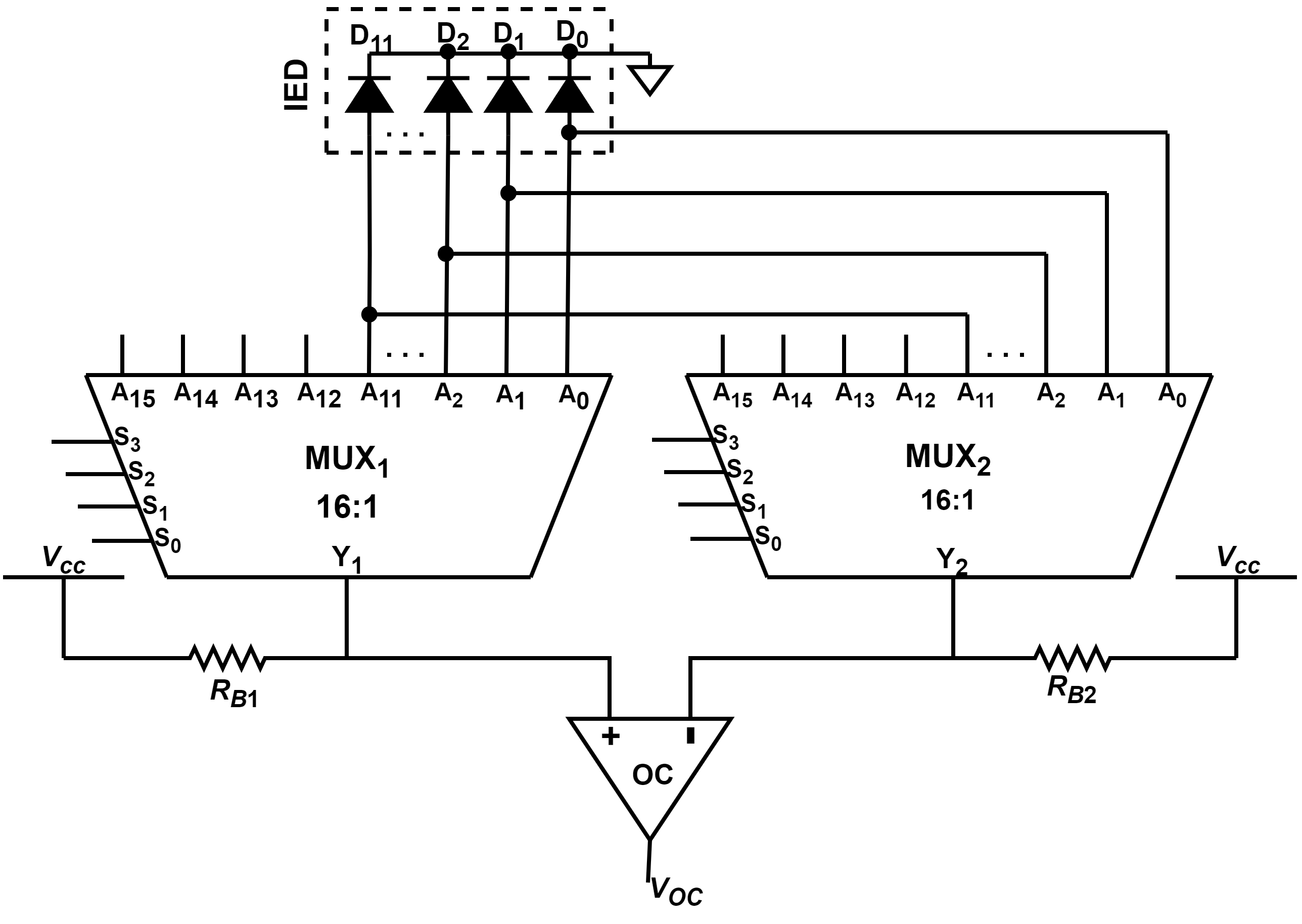
Our approach considers the diode cut-in voltage region and associated combinations of diode pairs. As mentioned earlier, twelve output relay ports, and thus, corresponding twelve diodes (, , …, ) were selected for measurement. and ( multiplexers) operate as analog multiplexer/demultiplexer. The diodes were connected to the terminals , , …, of and as in Fig. 1. The terminals and of and were pulled to the supply voltage using the resistors and . Under this configuration, when one of the terminals (say, ) of is connected to , (through appropriate logic levels at the multiplexer selector pins), a finite current (say, ) flows to forward bias the diode . Similarly, using , one of the other diodes (between to ) can be forward biased. The terminals and were directly connected to a low offset voltage ( mV) differential comparator chip (OC) as shown in Fig. 1.
Under the aforementioned setup, the twelve diode voltages were successively compared to those of the other eleven diodes. As a result, we will get diode comparisons (where in this case). A 1-bit output will be produced for every comparison. Let us consider one instance to elaborate this. The terminals of and of were selected for comparing the cut-in region voltages of a diode-pair, say and . Under this setting, the voltages at Y1 and Y2 terminals are, ideally, equal to the voltages (say, and ) across and . The comparator output can be expressed as:
The procedure was repeated and was compared to the diode voltages to to generate a 11-bit signature. Repeating the above procedure, each diode was compared with the remaining diodes. Thus, considering twelve output ports of the IED, or 132-bit signature was formed. The recorded bit-streams (say, and ) for two such IEDs are shown below. The signatures are expected to be unique to the individual IEDs under investigation.
III-A3 IED Regulated Voltages and Internal Oscillator Clock Period
The SEL-311C IED offers a serial port API to extract and display the clock period (say, ) and internal regulator voltages (say, ) of the IED. The IED SEL-311C contains three internal voltage regulators with nominal voltages of 3.3 V, 5 V, and 15 V. However, actual voltages may exhibit slight deviations due to fabrication process variations across regulator chips. As a result, can serve as potential PUF sources for different IEDs. Furthermore, the time period of the internal oscillator within the IED was extracted through serial communication using appropriate commands. The nominal value of is 20 nS. The deviation of is anticipated to be distinct for each IED, and thus presenting an additional parameter suitable for PUF generation.
|
|
|
|
|
||||||||||
|---|---|---|---|---|---|---|---|---|---|---|---|---|---|---|
| IED-1 | 3.26 | 4.95 | 14.85 | 19.999945 | ||||||||||
| IED-2 | 3.29 | 4.99 | 14.86 | 20.000063 |
III-A4 Signature Extraction from Regulated Voltages and Clock Period
In order to affirm the uniqueness of the regulated three voltages (, , and ) and , two SEL-311C IEDs were tested. Table II shows the results for this comparison. The regulated voltages and values were recorded over serial terminal a few hundred times to check the repeatability, and thus affirming their viability as distinctive characteristics for PUF-based applications. Table II reveals that the uniqueness in the regulated voltages and values for the two IEDs can be observed in their deviations (say, and ) from the respective nominal values. For example, in the case of IED-1, mV, mV, and mV. On the other hand, for IED-2, the corresponding values for , , and are 10 mV, 10 mV, and 140 mV, respectively. Similarly, values for the two IEDs are measured as 55 femtoseconds (fs) and fs, respectively. Signatures were formed using these parameters by converting the absolute decimal values of , , , and to corresponding binary (disregarding order information such as units (e.g., mV, fs) and any trailing zeros in the values). Additionally, an extra bit was added to the left of each binary code (as the most significant bit (MSB)) to denote polarity, with a 1 indicating a negative value and 0 representing a positive value. For instance, values of 55 fS and fS were transformed into binary as 0110111 and 1111111, respectively. Similarly, the values were also converted to binary, and finally, all the four parameters were concatenated in the same order as presented in Table II. The resulting 22-bit signatures for the two IEDs are illustrated below.
III-B Working Circuit for probe
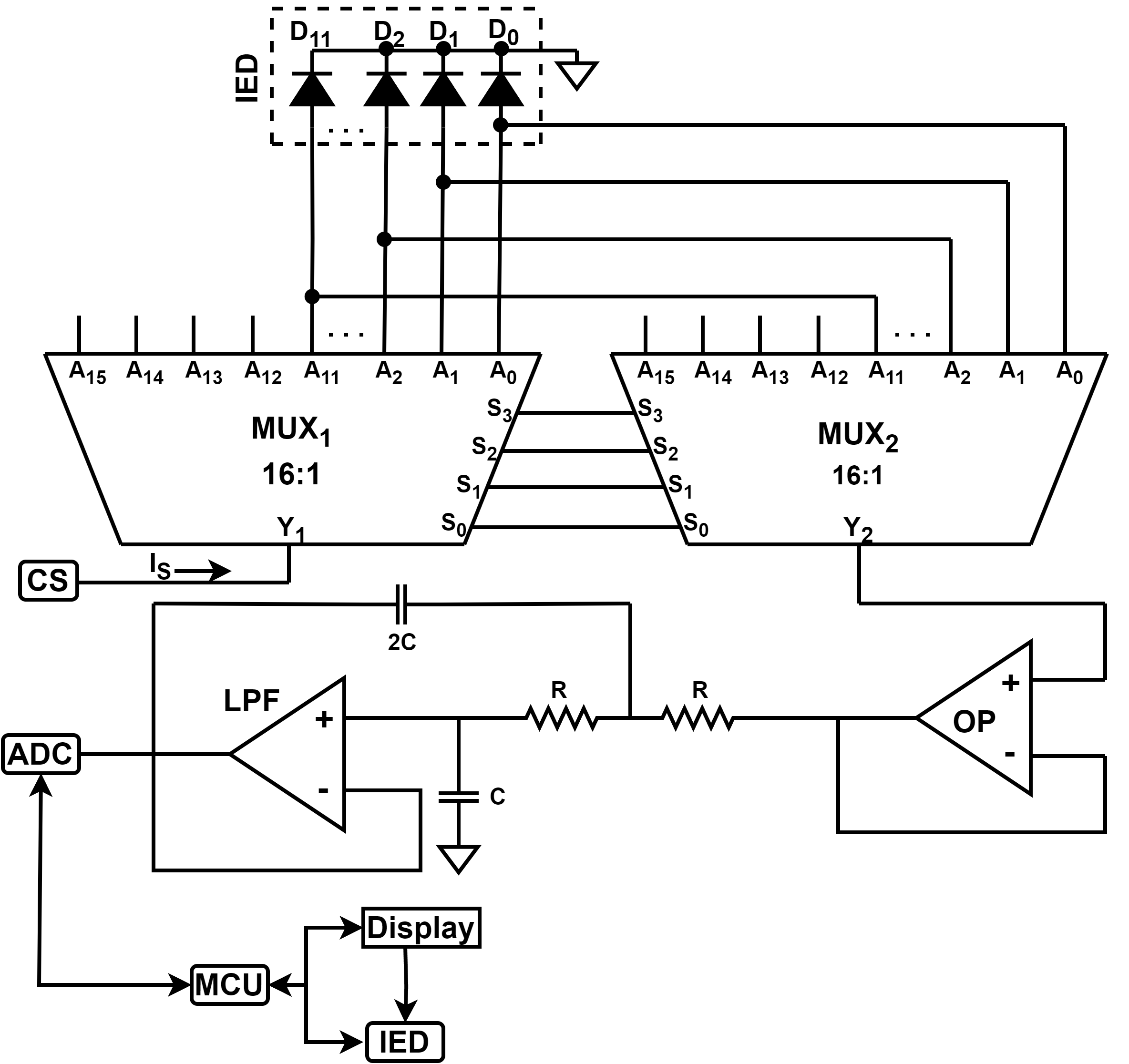
Earlier, in Section III-A2, a basic circuit schematic for extracting signatures from the twelve output port diodes (, , …, ) of a SEL-311C IED was presented. The measurement principle was simple. In the working circuit we address issues, such as high on-resistance (say, ) of the multiplexer switches, offset voltage of comparator, mismatches in the resistors and , variation of with power-supply and temperature changes.
The system-level schematic of the working probe is shown in Fig. 2. It incorporates various electronic hardware modules, including analog multiplexer/demultiplexer ( and ), an ADC, a microcontroller unit (MCU), a constant current source (CS), and a display unit. Similar to Fig. 1, twelve diodes (, , …, ) are connected to the inputs (, , …) of . In this design, the diodes are forward biased by a constant current (say, ) generated by the CS. The CS unit utilizes a precision reference voltage and a PNP transistor-based configuration [17]. As shown in Fig. 2, flows from the terminal of to the terminals , through , sequentially. The selection of channels is controlled by applying appropriate logic levels to the selector pins to .
The voltage (say, ) at the terminal of is related to the voltages across the diodes. However, also contains a component related with the voltage drop () across the internal resistance () of caused by the current flowing through . The component is significantly high and depends on temperature and power supply variations. To address this issue, has been introduced. The selector pins of and are tied together, as in Fig. 2, ensuring the selection of the same channels in both and during channel sweeping. The terminal of is connected to an op-amp (OP)-based voltage follower circuit. By leveraging the low bias current of the op-amp, the effect of is compensated.
The output of the op-amp is then passed through a simple second-order low-pass filter before being fed into a high-resolution ADC. The cutoff frequency of the filter is set at approximately 15 Hz. From Table I, it can be observed that the differences among the diode voltages can be of the order of 1 mV or even lower. As a result, selection of a suitable ADC is crucial for accurately resolving these voltages. Moreover, the measured diode voltages are static in nature. Considering these, a DC optimized Delta-Sigma (-) ADC is selected as will be detailed in Section V-A.
As mentioned in Section III-A3, the regulated voltages and parameters of the IED were acquired through serial terminal. The deployed MCU performs this serial communication operation with the IED and is also responsible for controlling other operations of the probe, such as applying appropriate logic levels to the multiplexer selector pins, managing the ADC & the display modules, implementing algorithms for signature extraction, and transmission operations.

IV Working Principle of probe
Fig. 3 depicts the authentication process for probe, as well as, the IED device. The signature extraction process involves a series of sequences executed when the CCS requests for IED signature extraction. The following steps outline this procedure:
-
1.
The CCS initiates communication by pinging the probe through the serial terminal.
-
2.
The probe and CCS execute Phase I, which involves verifying the authentication of the IED access request originating from the CCS, as well as, authenticating the probe.
-
3.
Upon successful authentication in Phase I, the CCS proceeds to Phase II by transmitting random port numbers (corresponding to the twelve output port under investigation) as challenges to the probe.
-
4.
The probe generates a response to the challenges presented by the CCS in Phase II. This response is then transmitted back to the CCS, where it undergoes further verification processes to authenticate the IED.
Phase I performs mutual authentication between the CCS and the probe. To accomplish this, we extract ADC PUF (ADCMCU) hardware signature using the procedure elaborated in [9]. Using this procedure, we estimate the mean () and standard deviation () of the 12-bit ADC present in the MCU. Phase II focuses on implementing a challenge-response-based mechanism to authenticate the IED on the CCS side. These two phases will be further elaborated in the subsequent subsections.
IV-A Phase I - Authenticating CCS
The Phase I starts with an initial authentication request issued by the CCS and ends with an authentication acknowledgement. Upon receiving the authentication request, the probe sends three parameters to the CCS: a randomly generated number , , and . These two ADC parameters are obtained from the ADCMCU PUF. The CCS compares these values with previously stored references. If the comparison yields a match, the authenticity of the probe is validated. Following this stage, the CCS transmits a hash value , generated using a MD5 hash function and as an input. The probe also generates its hash response to the same input . and are compared for a match to authenticate the CCS access request. Conversely, if and do not match, the Phase I is deemed unsuccessful, and access is denied. The aforementioned sequences are illustrated under Phase I in Fig. 3.
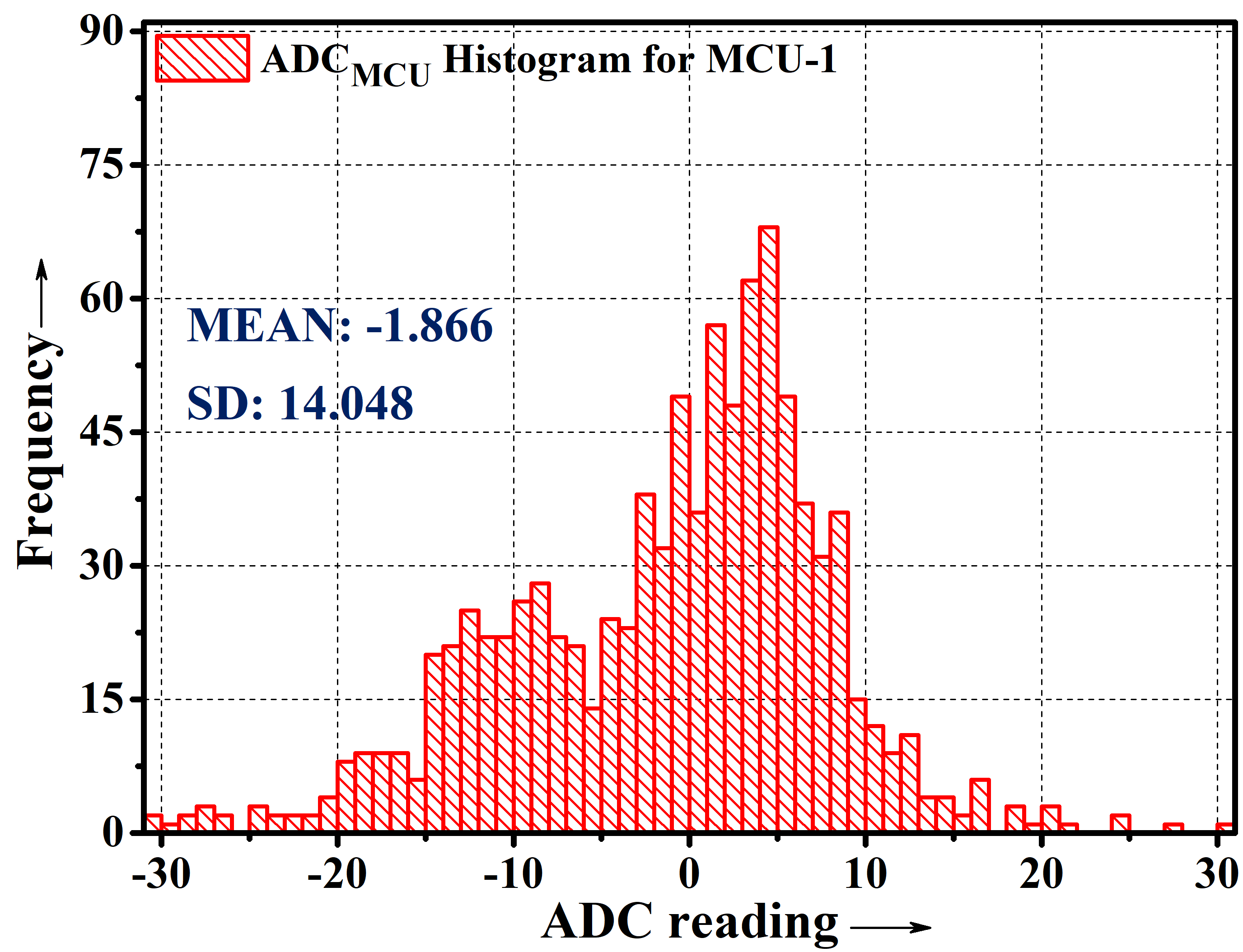
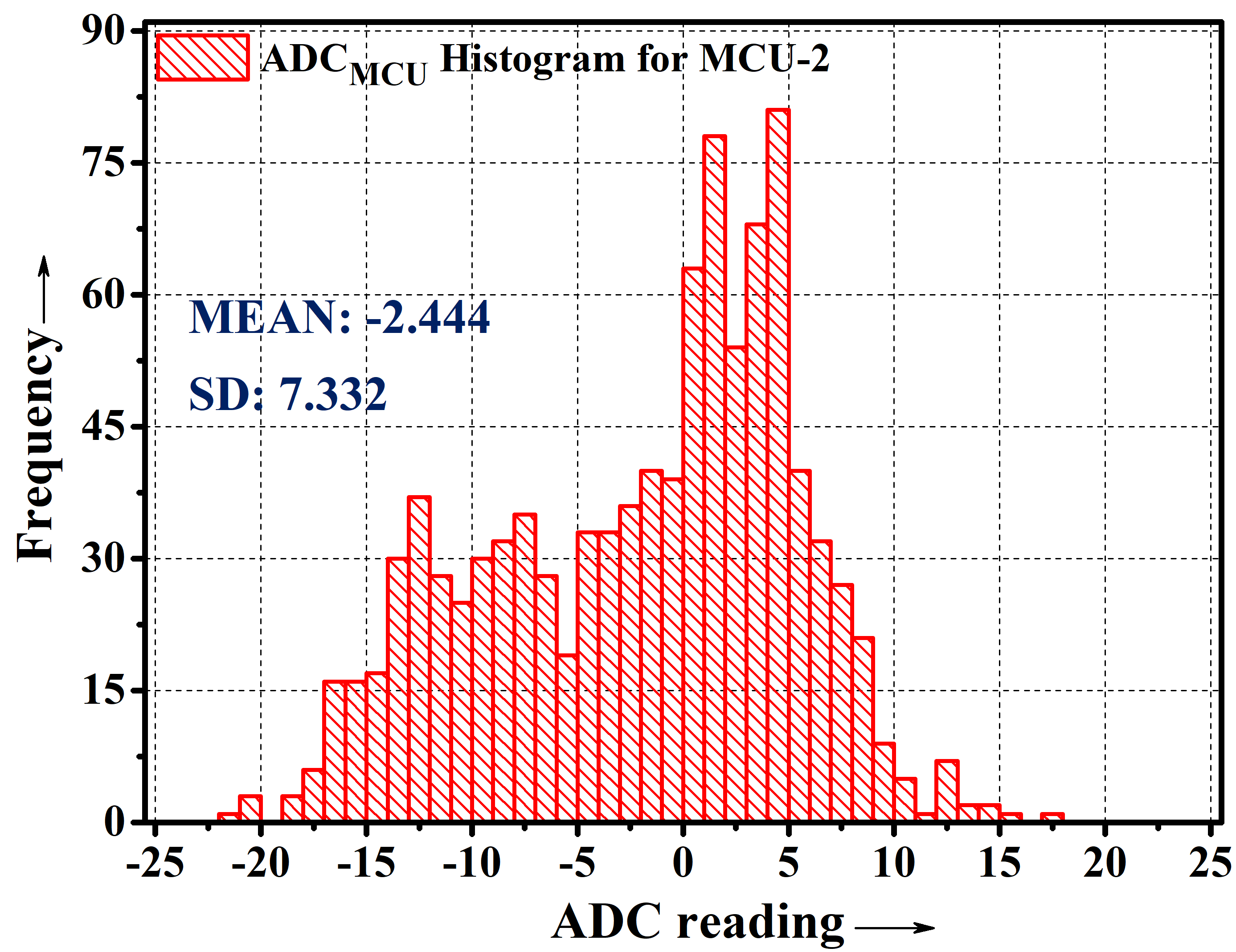
Figs. LABEL:ADC1 and LABEL:ADC2 show that the histogram of ADC output values for two identical MCU devices. The measurements were taken over 10,000 samples in differential mode. and values, indicated in the figures, demonstrate uniqueness for the two MCU devices.
IV-B Phase II - Authenticating IED
Upon successful completion of Phase I, the CCS proceeds with the authentication of the IED as shown under Phase II of Fig. 3. As mentioned previously, the CCS securely stores reference signatures () of all IEDs in its database. For the authentication process, the CCS transmits a random challenge () to the probe, consisting of random port numbers (say, where for ). The different values corresponds to a port number, between Port 1 to Port 12. The number of ports challenged in each will vary randomly, such as challenging eight ports in one instance and all twelve ports in another. After issuing the challenge, the CCS will generate an anticipated response () from its database of reference signatures, which includes the following relevant data of the corresponding IED device: (i) clock period (), (ii) three regulated voltages (, , and ), and (iii) a partial bit-stream, formed by utilizing the known and the reference . Upon receiving , the probe will retrieve the signatures from the IED. Subsequently, it will generate a bit-stream specific to the challenged ports and combine it with the and signatures, forming the response which is transmitted back to the CCS. The CCS compares with to authenticate the IED.
V Experimental Evaluation
V-A Experimental Setup
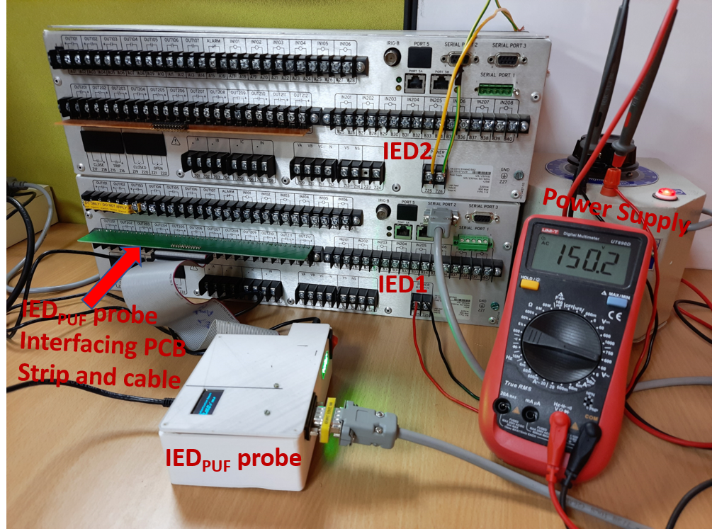
Fig. 5 shows the complete experimental setup employed for the characterization and authentication of an SEL-311C IED using the proposed probe. As previously mentioned, twelve output ports of the IED are chosen for signature extraction, utilizing the protection diodes and a dedicated PCB strip facilitates this process. To establish the connection between the probe and the IED, a flat-ribbon cable and the aforementioned PCB strip are employed. The MCU module is implemented using an NRF52840-based microcontroller unit. and are designed using CD4067-based analog multiplexers. Furthermore, the ADC module has been implemented utilizing the ADS1115 16-bit - converter. The serial communication between the probe and the IEDs are realized through an RS232 to TTL serial interface module. The CCS is implemented on a laptop computer, and the algorithms on the CCS side are coded in Python.
V-B Experimental Results
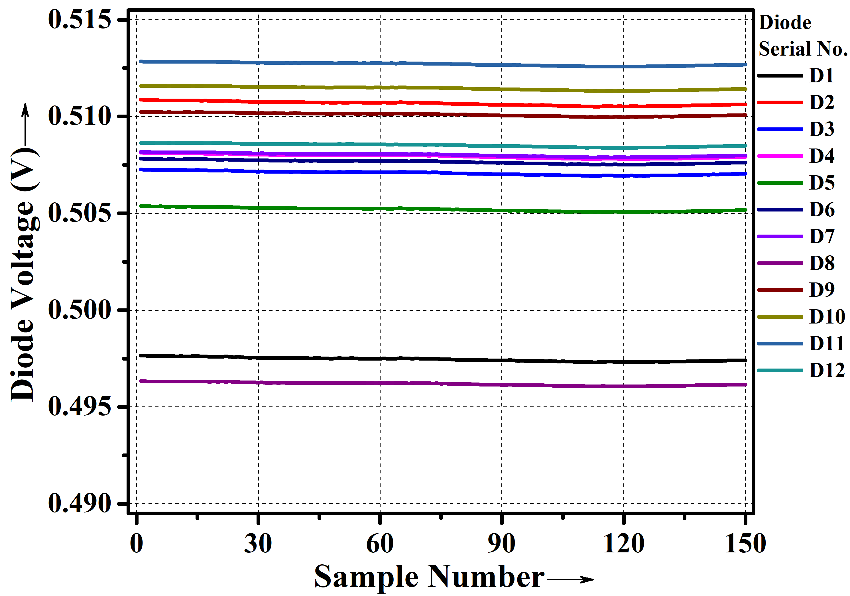
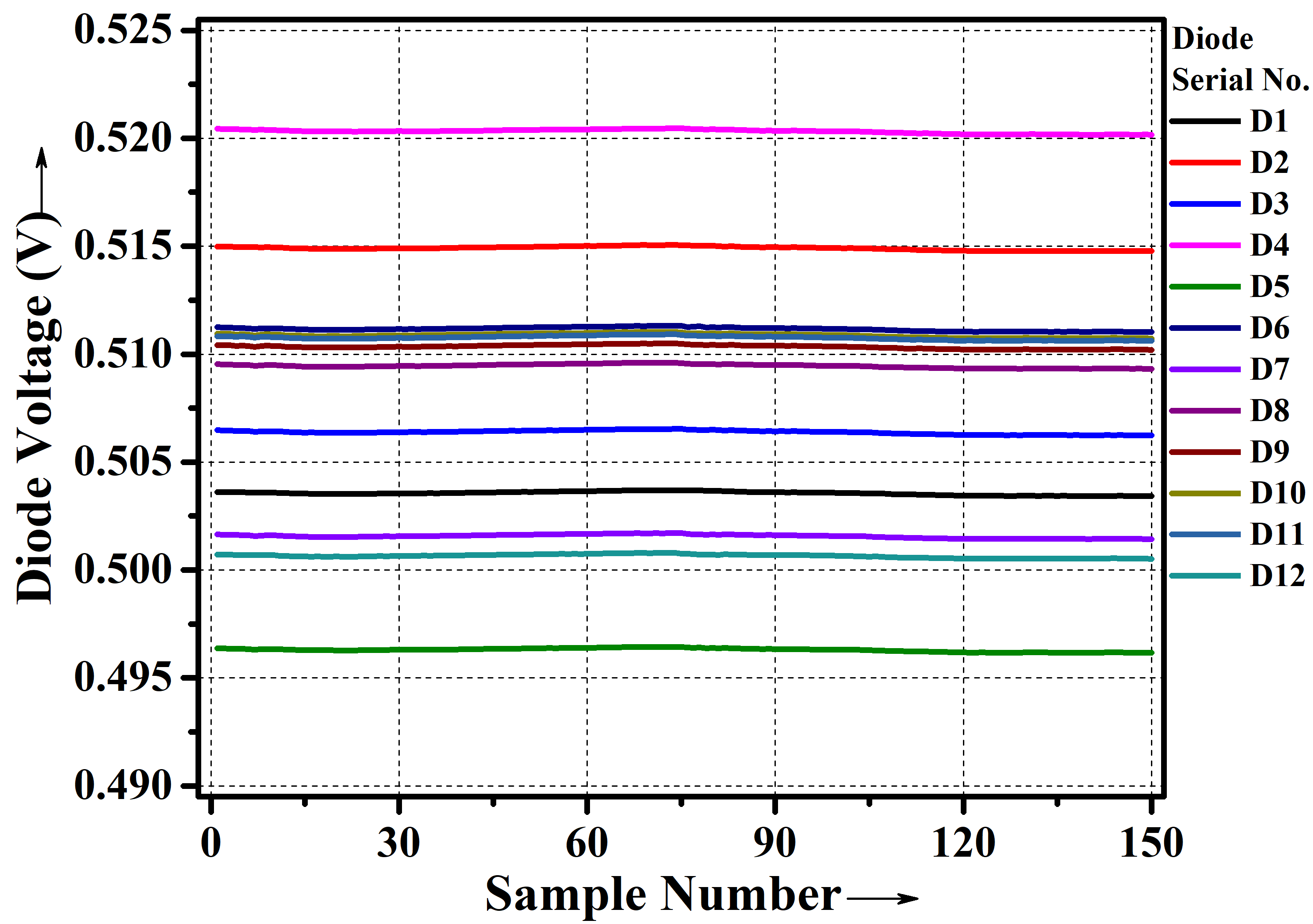
The experiments were conducted with two commercial SEL-311C IEDs, as previously mentioned. Preliminary results for these IEDs are illustrated in Fig. 6. These figures display the diode voltages obtained from continuous acquisition of 150 samples at a constant current of mA. The twelve diode voltages of IED-1, shown in Fig. LABEL:IED1basic, exhibit variations within the range 495 mV to 513 mV. On the other hand, IED-2 demonstrates diode voltage variations ranging from 495 mV to 520 mV. It can be observed that in Fig. LABEL:IED1basic, 11 of the 12 line-plots are distinctly visible, while in Fig. LABEL:IED2basic, 10 lines are distinct. This indicates the presence of collisions in very few of the diode voltages for both IEDs. Moreover, the horizontal characteristics of the line-plots affirms excellent repeatability in the measurements.
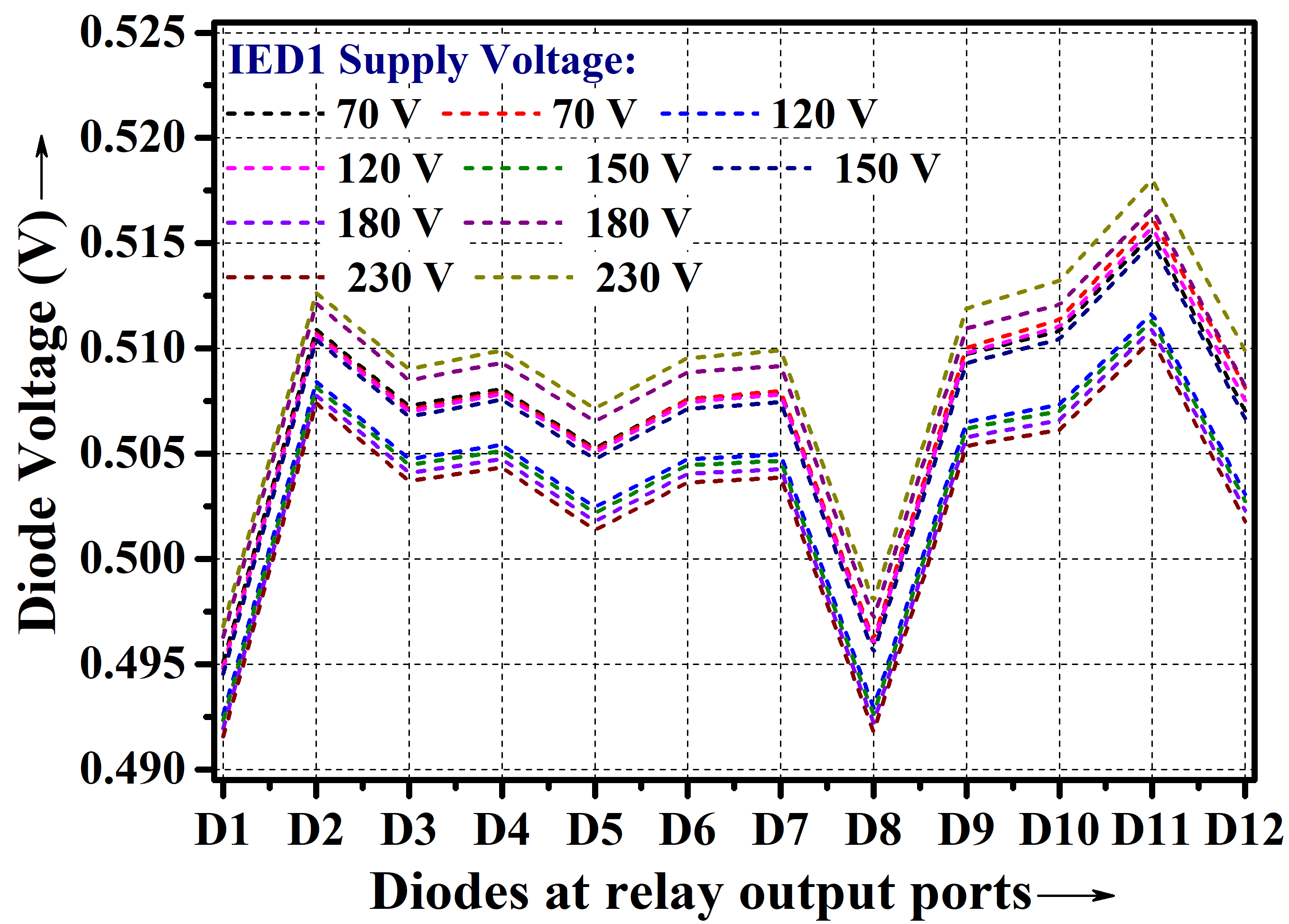
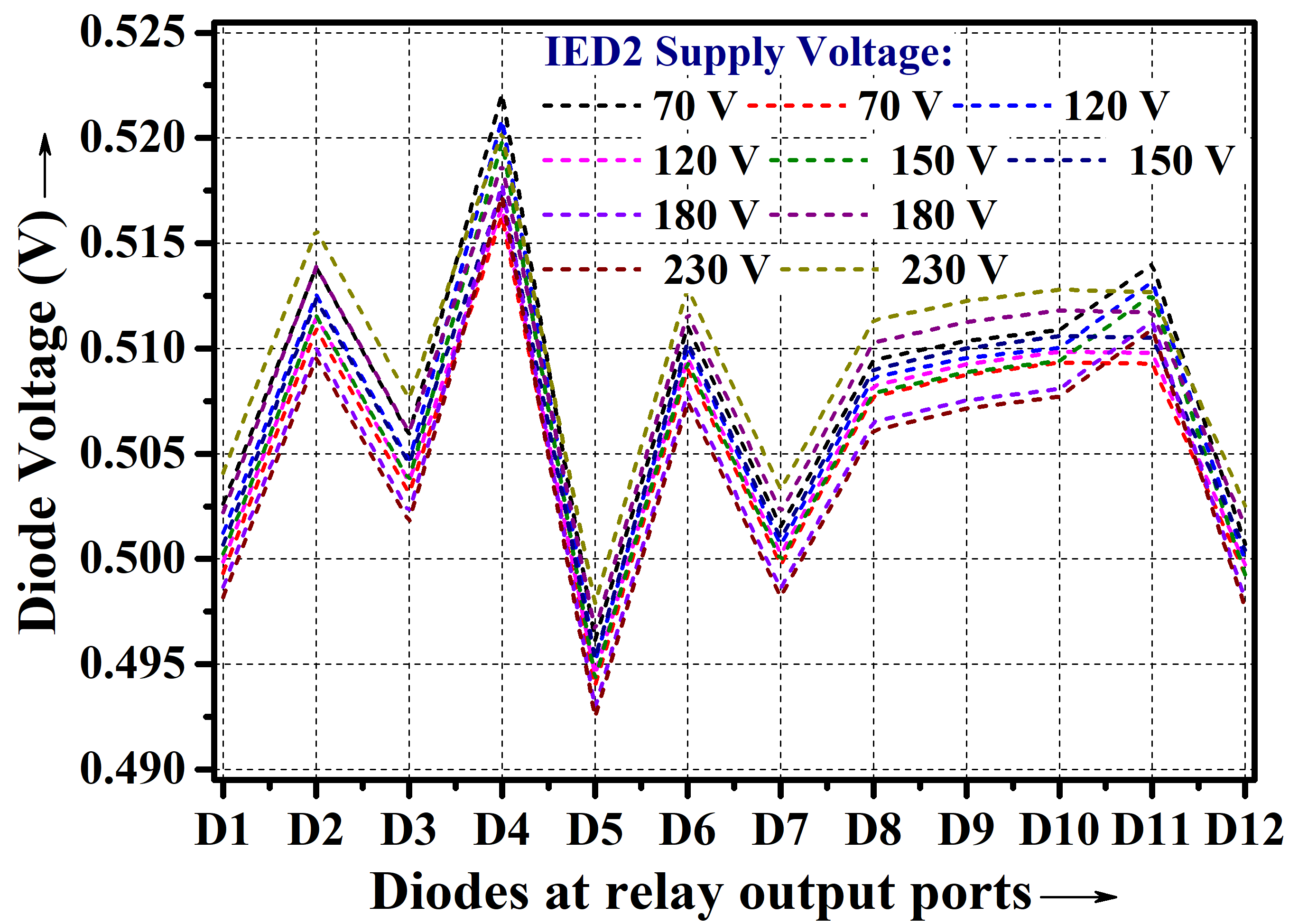
Fig. 7 further clarifies the diode signature patterns for the two IEDs. The results in Fig. 7 were obtained by monitoring the diode voltages over a span of two weeks. During this experiment, the power supply of the IEDs was varied over 70 V to 230 V to study the robustness of the signatures. Fig. LABEL:IED1voltage and LABEL:IED2voltage present the worst-case variations observed in the diode voltages for the two IEDs. It is evident from these plots that the characteristics of the two IEDs exhibit distinctive patterns, signifying their uniqueness.
In order to examine the robustness performance of the , the following common metrics [13] of PUF signatures are assessed. These parameters are evaluated using the full 154-bit PUF signature derived from the datasets of Fig. 7.
-
1.
Uniqueness: This parameter is determined by assessing the inter-device variation. This involves performing an XOR operation on the bit-strings obtained from two separate IEDs, summing the result, and then the sum is divided by the length of the bit-strings. The desired value for inter-device variation is 0.5. The worst-case values of uniqueness between IED-1 and IED-2 were evaluated to be approximately 0.31.
-
2.
Stability: Intra-device variation quantifies this parameter. To evaluate stability XOR operation is performed on two bit-strings measured from a particular IED, the result is summed and the sum is divided by the length of the bit-string. Ideally, the intra-device variation is expected to be zero. The worst-case values of stability for IED-1 and IED-2 were found to be 0.09 and 0.06, respectively.
-
3.
Bias: Bias is calculated by dividing the sum of the bit-string by the length of the bit-string. The desired bias value is 0.5. The bias for the signatures of IED-1 and IED-2 were determined to be 0.51 and 0.52, respectively.
| S1 | S2 | S3 | S4 | S5 | S6 | S7 | S8 | S9 | S10 | S11 | S12 | |
|---|---|---|---|---|---|---|---|---|---|---|---|---|
| D0 | 843 | 825 | 830 | 828 | 844 | 820 | 859 | 798 | 830 | 864 | 817 | 842 |
| D1 | 800 | 843 | 835 | 861 | 836 | 861 | 830 | 841 | 865 | 826 | 806 | 796 |
| D2 | 824 | 801 | 864 | 873 | 772 | 816 | 880 | 814 | 818 | 848 | 836 | 854 |
| D3 | 836 | 847 | 794 | 855 | 793 | 783 | 886 | 853 | 836 | 830 | 798 | 889 |
| D4 | 868 | 810 | 823 | 820 | 839 | 859 | 785 | 863 | 817 | 800 | 850 | 866 |
| D5 | 828 | 821 | 849 | 843 | 859 | 844 | 825 | 848 | 812 | 822 | 832 | 817 |
| D6 | 854 | 851 | 831 | 788 | 842 | 795 | 824 | 847 | 824 | 859 | 857 | 828 |
| D7 | 851 | 836 | 827 | 811 | 887 | 848 | 817 | 848 | 788 | 840 | 826 | 821 |
| D8 | 794 | 851 | 855 | 836 | 823 | 854 | 784 | 831 | 869 | 814 | 853 | 836 |
| D9 | 811 | 902 | 795 | 835 | 823 | 853 | 852 | 823 | 845 | 804 | 824 | 833 |
| D10 | 851 | 769 | 870 | 836 | 863 | 812 | 837 | 834 | 788 | 854 | 872 | 814 |
| D11 | 840 | 844 | 827 | 814 | 819 | 855 | 821 | 800 | 908 | 839 | 829 | 804 |
In addition to these parameters, the randomness of the signatures can be evaluated by measuring the entropy, which can be estimated from the data in Table III. As described in Section IV-B, CCS challenges the probe with a sequence of twelve random port numbers denoted as S1, S2, …, S12 in Table III. About 10,000 sequences were generated to evaluate the randomness. In the table, the first row labeled D0 represents the number of occurrences of the diode D0 in the sequence positions S1, S2, …, S12 across the challenges. Similarly, the rows labeled D1, D2, and so on, represent the occurrences of diodes D1, D2, and subsequent ones. The entropy (say, ) of the sequence at the -th position can be calculated using the formula: , where is the probability of occurrence of the -th diode appearing in . The maximum entropy () for any occurs when , resulting in . On evaluation of the entropies for S1, S2, …, S12 from Table III, all entropy values were approximately equal to , with an error of less than .
VI Conclusion
This paper introduces a hardware-level security solution specifically designed for commercial IEDs. The solution incorporates (PUF)-based techniques to extract unique signatures from the IEDs. The primary objective of this study is to enhance the security of IEDs, mitigating the risks associated with counterfeiting. In this work, the probe has been presented as a complete solution, encompassing both its hardware architecture and software development. The proposed probe is a simple, low-cost embedded device that can be easily customized to accommodate various IED models. To validate the effectiveness of the proposed probe, extensive experimental evaluations have been conducted, yielding promising results. Additionally, the experimental results highlight the scopes for further PUF hardening against external variations like power supply and aging. As part of our future work, we intend to focus on addressing these challenges and exploring the extraction of signatures from IEDs of different manufacturers.
References
- [1] S. Hussain, J. H. Fernandez, A. K. Al-Ali and A. K. Shikfa, “Vulnerabilities and Countermeasures in Electrical Substations,” in Int. J. of Critical Infrastructure Protection. 33, 2021.
- [2] J. Wang and D. Shi, “Cyber-Attacks Related to Intelligent Electronic Devices and Their Countermeasures: A Review,” Int. Univ. Power Engg. Conf. (UPEC), Glasgow, UK, 2018, pp. 1-6.
- [3] The Open Group. “ISO/IEC 20243-1:2018” iso.org. https://www.iso.org/standard/74399.html (accessed May 22, 2023).
- [4] S. Joshi, S. P. Mohanty and E. Kougianos, “Everything You Wanted to Know About PUFs,” in IEEE Potentials, vol. 36, no. 6, pp. 38–46, Nov.-Dec. 2017.
- [5] J. R. Hamlet et al. “Deterrence of device counterfeiting, cloning, and subversion by substitution using hardware fingerprinting,” US 8,848,905, Sept. 30, 2014, https://www.osti.gov/biblio/1159918, Accessed on May 22, 2023. [Online].
- [6] J. W. Lee, et al., “A technique to build a secret key in integrated circuits for identification and authentication applications,” Symp. on VLSI Circuits. Digest of Technical Papers, Honolulu, USA, 2004, pp. 176–179.
- [7] G. E. Suh and S. Devadas, “Physical Unclonable Functions for Device Authentication and Secret Key Generation,” ACM/IEEE Design Automation Conf., San Diego, CA, USA, 2007, pp. 9–14.
- [8] A. Duncan, L. Jiang and M. Swany, “Repurposing SoC analog circuitry for additional COTS hardware security,” IEEE Int. Symp. on Hardware Oriented Security and Trust (HOST), Washington, DC, USA, 2018, pp. 201–204.
- [9] G. Vaidya, A. Nambi, T. V. Prabhakar, V. Kumar T and S. Sudhakara, “IoT-ID: A Novel Device-Specific Identifier Based on Unique Hardware Fingerprints,” IEEE/ACM 5th Int. Conf. on IoT Design and Implementation (IoTDI), Sydney, NSW, Australia, 2020, pp. 189-202.
- [10] D. Holcomb, W. Burleson and K. Fu, (2007). “Initial SRAM State as a Fingerprint and Source of True Random Numbers for RFID Tags,” Proc. Conf. RFID Secur., vol. 7, pp. 1-12, Jan. 2007.
- [11] G. Vaidya and T. V. Prabhakar, “Hardware based identification for Intelligent Electronic Devices,” IEEE/ACM 7th Int. Conf. on IoT Design and Implementation (IoTDI), Milano, Italy, 2022, pp. 82-94.
- [12] G. Vaidya, T. V. Prabhakar and L. Manjunath, “GPIO PUF For IoT Devices,” IEEE Global Comm. Conf., Taipei, Taiwan, 2020, pp. 1-6.
- [13] J. R. Hamlet, M. T. Martin and N. J. Edwards, “Unique signatures from printed circuit board design patterns and surface mount passives,” Int. Carnahan Conf. on Security Tech. (ICCST), Madrid, Spain, 2017, pp. 1-6.
- [14] N. J. Edwards et al. “Authenticating a Printed Circuit Board,” US 10,594,492, Jun 16, 2017, https://www.osti.gov/biblio/1637851, Accessed on May 22, 2023. [Online].
- [15] M. Ebrahimabadi, M. Younis and N. Karimi, ”Hardware Assisted Smart Grid Authentication,” ICC 2021 - IEEE International Conference on Communications, Montreal, QC, Canada, 2021, pp. 1-6.
- [16] Schweitzer Engineering Laboratories. “SEL-311C Protection and Automation System.” selinc.com. https://selinc.com/api/download/3032 (accessed May 22, 2023).
- [17] Texas Instruments, “LM185/LM285/LM385 Adjustable Micropower Voltage References,” LM385 datasheet, Feb. 2000 [Revised April. 2013].