High-definition event frame generation using SoC FPGA devices
Abstract
In this paper we have addressed the implementation of the accumulation and projection of high-resolution event data stream (HD – pixels) onto the image plane in FPGA devices. The results confirm the feasibility of this approach, but there are a number of challenges, limitations and trade-offs to be considered. The required hardware resources of selected data representations, such as binary frame, event frame, exponentially decaying time surface and event frequency, were compared with those available on several popular platforms from AMD Xilinx. The resulting event frames can be used for typical vision algorithms, such as object classification and detection, using both classical and deep neural network methods.
I Introduction
Event cameras (DVS – Dynamic Vision Sensors) are state-of-the-art vision sensors inspired by biology. They only detect changes in brightness in an image and can operate with microsecond resolution. For this reason, they are able to register changes in the environment very quickly, i.e. they have low latency. In addition, they operate correctly under difficult lighting conditions, e.g. limited brightness or high dynamic range. The aforementioned properties make DVS an interesting sensor for currently developing autonomous vehicles, including drones, where both speed of operation and robustness to a variety of lighting conditions are important.
However, processing event data, which is in the form of a sparse spatio-temporal cloud, is challenging. Several approaches are encountered in the literature: from the direct analysis of the point cloud, to the projection of events onto a plane (representations) and reconstruction [1]. Particularly popular is the use of a representation in the form of a so-called event frames, i.e. events collected over a certain time interval, projected onto the image plane. This allows the use of typical, well-known vision algorithms – both classical and those based on deep learning.
In order to process event data quickly enough, a powerful hardware platform is needed on which relevant information can be extracted in real-time, e.g. the position and direction of potential objects in the drone’s environment. This prerequisite is met by SoC FPGA (System-on-Chip Field Programmable Gate Array) or embedded GPU (embedded Graphics Processing Unit) platforms, which enable parallel computing and, in addition, are small and lightweight and therefore well suited to be placed on a drone.
In this paper, we address the subject of event frame generation in SoC FPGAs for data in HD (High Definition – pixels) resolution or higher. To the best of our knowledge, this issue has not yet been considered in the scientific literature for such high resolutions (Section II-B) and it presents many challenges, both scientific (hardware architecture development) and technical (implementation).
The remainder of this paper is organised as follows. Section II provides background information on event cameras and the approaches available in the scientific literature to the problem considered. Section III is devoted to the presentation and comparison of different event data representations. Details of the hardware implementation of the algorithm, together with its potential enhancements, are collected in Section IV. The final Section V summarises the work done and indicates further directions for development.
II Event-frame generation
II-A Event camera
Dynamic Vision Sensors differ from traditional frame cameras in both design and operation. Firstly, they only record brightness changes independently (asynchronously) for each pixel. Each such change is called an event and consists of four pieces of information: the exact time of occurrence (timestamp), the and positions in the image, and the polarity, i.e. information about the increase or decrease in brightness (positive and negative polarity respectively), which can be written as .
When monitoring a static scene, event cameras do not transmit any data (apart from noise), which significantly reduces data transfer and energy requirements. Secondly, changes are recorded at a very high rate – more than a thousand times per second, whereas frame cameras typically operate at lower frequencies (e.g. 30, 60, 120 or up to 240 frames per second). Another difference resulting from this is the significant reduction in blur effect associated with object movement on event data, which enables correct registration of a highly dynamic scene. A fourth advantage over traditional cameras is the high dynamic range, allowing very bright and very dark areas to be recorded in a single image, which is usually not possible with frame cameras.
II-B Previous works
A number of solutions can be found in the scientific literature where frames were generated to perform certain tasks based on event data. The paper [4] realised traffic sign detection using neural networks and proposed a multi-channel approach (different simple representations on three image channels). The work [7] proposed a system for object detection using neural networks and a representation based on the frequency of event occurrence. The paper [8] presented a system for pedestrian detection using a neural network and a representation called neighbourhood suppression time surface. For the gesture recognition task, a temporal binary representation method was proposed in [9], where a sequence of 8 binary frames was generated, aggregated to a single greyscale image. The only work where frame generation was done for HD data is [5], which proposed a system to control the flow of elements in time (falling corn grains).
One of a few similar hardware implementations on an FPGA platform is [10], whose authors performed object classification using a NullHop accelerator based on a convolutional neural network. In this work, frames were generated for a specific number of events instead of a time interval. Two memory blocks for data of only elements were used, so the authors did not encounter a number of challenges in implementing the algorithm for high-resolution data.
The generation of frames without distinguishing events’ polarity was part of the optical flow determination algorithm on an FPGA platform [11], in which data was accumulated in 3 blocks from consecutive time intervals. In the project an event camera with a resolution of pixels was used.
The work [12] developed a gesture recognition system using an FPGA platform and a hierarchy of time surfaces representation, inspired by an approach from multi-layer neural networks, and a single-layer linear decay kernel representation, i.e. linear decay of events in time. Each single event was specified using the time context concept, a quadratic matrix of timestamp differences in a small neighbourhood. In the project two event sensors (with and pixels resolutions) were used, but for the purposes of the algorithm, the data was stored in an accumulator scaled to .
In summary, in a number of research papers projecting event data onto the image plane using different representations was proposed, and further processing of the frames was rather performed using neural networks than classical methods. In some of these papers, an FPGA platform was used for the implementation of the frame generation algorithm, but for very low resolution data. The implementation of such an algorithm for high-resolution data has not yet been addressed as it raises several problems, mainly related to the handling of incoming events and real-time frame generation, which at low resolutions – due to much less data per time interval – simply do not occur. This paper therefore attempts to fill this gap, which becomes particularly relevant as the resolution of commercially available event cameras increases – from pixels in 2008 up to in 2020 [6].
III Event-frame representations
There are several approaches to processing event data, e.g. ‘straightforward’, which requires the development of new algorithms due to the different data format. Therefore, a more ‘natural’ approach is the generation of so-called event frames, which consist of events from certain time intervals projected onto a plane, resulting in pseudo-images similar to these of traditional frame cameras, to which well-known algorithms can be applied. However, the frame generation poses a number of challenges: selecting the event accumulation period, taking into account time information when projecting onto the plane or ensuring real-time frame generation and further processing.
To date, several basic data representations for event frame generation have been proposed in the literature, with additional modifications for specific applications. According to [13], a function can be defined that assigns the time of occurrence of an event to each coordinate pair , and a function that assigns a polarity from the set or, using another convention, . In addition, a parameter can be defined, indicating the event accumulation time for the generation of one frame. The representations listed in this section are defined (for simplicity) for times .
III-A Binary frame
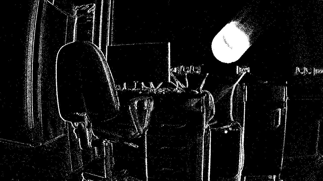
The first representation – for maximum simplicity – can be a binary information about the occurrence of an event in given coordinates, as in [11]: . A binary frame can also be generated from events of only one polarity.
III-B Event frame
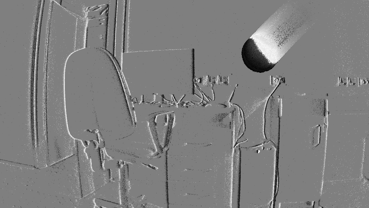
The second approach is a slight modification of the previous one, as the polarity of events is taken into account, according to the work [14]: . This is one of the most popular representations due to its simplicity, but also the considerable amount of information it contains.
III-C Exponentially decaying time surface
In this representation the temporal information is taken into account, precisely by specifying the time from the event occurrence to the end of the accumulation period, as in [14]. This value is then used for determining the brightness of a pixel in the resulting image: . This is motivated by the observation that the weight of information contributed by an event decreases with time to 0.
III-D Event frequency
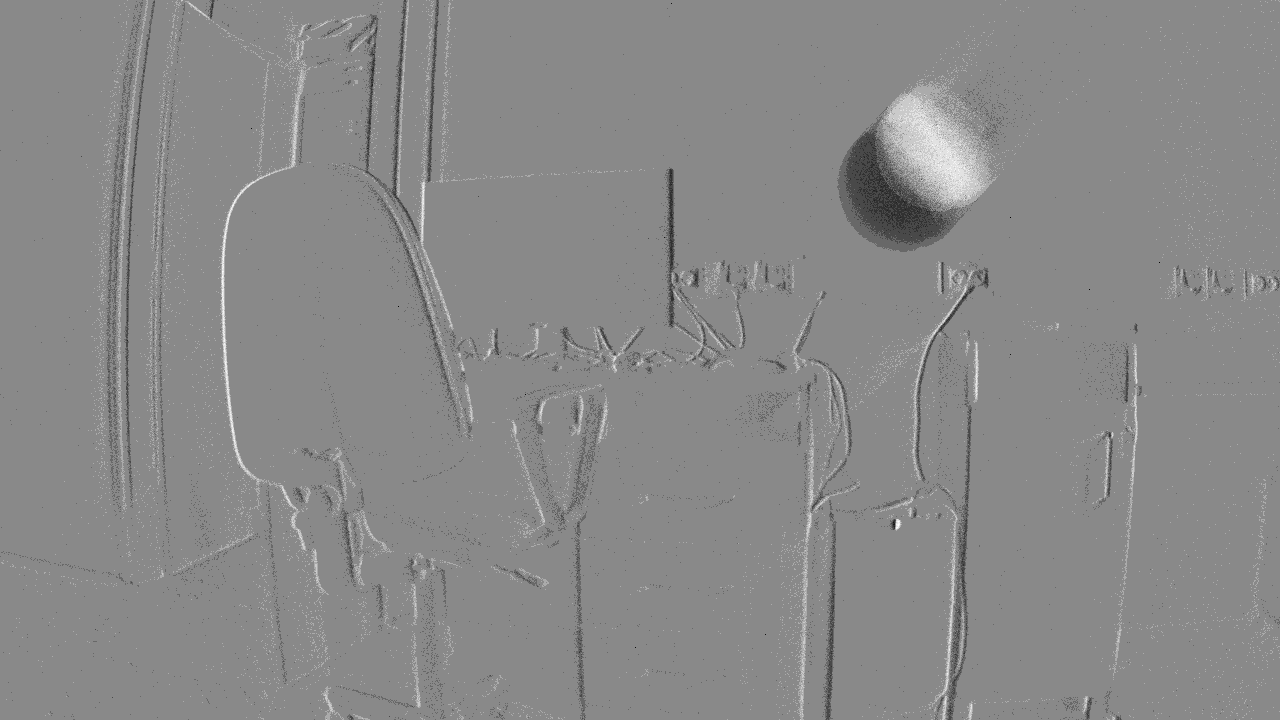
The next approach uses information about the frequency of a given pixel in the image, as proposed in [7]: , where the sum of polarisations for a pixel is denoted as .
III-E Comparison
A comparison of generated event frames using the representations described is shown in Figure 1. An exemplary sequence shows a fast-moving ball flying through a room recorded by a moving event camera. Apart from aforementioned representations, more complex arithmetic operations can be proposed to determine the values of individual pixels, as mentioned in Section II-B. There are also solutions in which an image with multiple channels of particular representations [4] or aggregated into one-channel [9] is generated.

IV The proposed frame generation module
In this work, we have developed several versions of a hardware module for event frame generation on an FPGA platform. Their architectures were prepared in SystemVerilog language using the Vivado environment and tested for AMD Xilinx’s FPGA platforms. The input of each module was an event and the output was an 8-bit pixel brightness value. For testing purposes, sample sequences with a thrown ball were recorded with a moving (rotating) Prophesee EVK1 camera in HD resolution. The events were saved to a text file, from which they were read in the Vivado simulation.
IV-A Basic version
The architecture of the basic version of the algorithm consists of three elements: a memory for storing accumulated events, logic controlling the reading and writing of data, and a temporary buffer for incoming data during frame reading.
The first of these elements can be realised in two ways – using the FPGA chip’s internal block memory (BRAM) or external RAM (usually dynamic). In the first case, the memory resources are quite limited, so the appropriate representation and resolution of the image must be selected. In the second case, the resources are much larger, but this approach increases the complexity of the architecture, introduces additional latency in data processing and is more energy consuming. Therefore, the first solution is used in this work due to its greater simplicity and operational efficiency. The number of elements in memory was set to 921600 (the number of pixels in an HD image). The number of bits allocated for one element depends on the chosen representation, but in the simplest case just 1 bit can be assumed (Section III-A). Other variants are described as algorithm extensions in Section IV-B1.
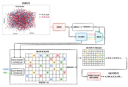
The second element is the logic that controls the communication with the two-port block memory, of which one port is used for writing data and the other for reading. As long as events belonging to a certain time interval (e.g. 10 ms) occur at the input, the algorithm operates in write mode. Based on the coordinates of the incoming event, the address in memory is determined as: , while the value stored equals 1.
When the condition to stop the write mode is met (e.g. value exceeded), the algorithm enters read mode, resetting the pixel position counter in the image. Its value is given as the address of the memory cell from under which the content of the accumulator is read before being incremented by 1. The value read is further decoded to the range 0-255 to display the output event frame in greyscale. At the same time, the address used for reading data is delayed by one clock cycle and fed to the input of the second port used for writing, together with the value 0, to reset the memory cell. When the counter reaches the last pixel in the image, the algorithm returns to write mode. A schematic visualisation of the operation of the algorithm in write and read mode is shown in Figure 2.
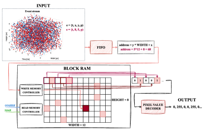
Due to event camera properties, just after entering the read mode, new events may appear at the input of the module, which should be used for the generation of the next frame. So the last necessary element is to handle these events. In order to separate the ‘older’ events (in the accumulator) from the ‘newer’ ones (at the input), a temporary buffer must be prepared to store them until the read mode finishes. It was realised as a FIFO (First In First Out) queue using the FPGA’s block memory, in which all event components were stored.
Regardless of the operation mode, each event was firstly written to the FIFO. Once in write mode, data was read from the queue and, in the meantime, the latest events from the input were written to the FIFO. A difficult issue is to determine the maximum size of the queue in order to store all incoming events but with low memory usage, as it depends on the dynamics of the scene and the value. In our solution, the queue size was set to 32768 elements. In addition, a mechanism of removing ‘the oldest’ events from the queue to add ‘the newest’ was implemented, if the FIFO was full in read mode. This was motivated by the fact that ‘newer’ events are more important, as they represent the most recent changes.
IV-B Extensions
The architecture described in Section IV-A is sufficient to correctly generate event frames in real-time on an FPGA platform. However, a number of enhancements and extensions can be applied to achieve better performance or results.
IV-B1 Other representations
The first element is another representation of event data. The simplest and most common modification is to add polarisation, creating an event frame. In this case, an event with a polarity of 1 generates an output pixel value of 255, the one with 1 polarity generates 0, while pixels without events receive a value of 128. To save hardware resources, a 2-bit value is stored in the accumulator, denoting 1 (positive event), 1 (negative event) or 0 (no event).
For other representations described in Section III, Look-Up-Table (LUT) can be used to store the approximate values of the exponential function. In the case of the method in Section III-C, knowing the value of (e.g. 10 ms), the difference between the current timestamp and the maximum value for the interval can be calculated. The rounded result can be stored in an 8-bit accumulator, thus obtaining the output pixel value.
For the representation from Section III-D, it was necessary to determine the maximum number of events for the given coordinates, which depends on dynamics of the scene and value. After tests on an example sequence, a limitation to the interval turned out to be sufficient, as larger polarity sums had no apparent effect on the final pixel value. Therefore, 5 bits were stored in the accumulator and then were decoded to an 8-bit output. The polarity counting itself was done in a way that with the arrival of a new event with the given coordinates, the current value was read from the accumulator using one port of the block memory, after which, depending on the polarity, the number 1 was added or subtracted and then written back to the same address using the other port.
IV-B2 Multiple Block RAMs
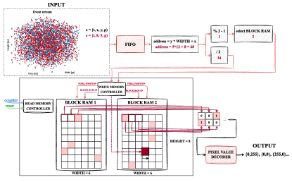
It is possible to use a set of smaller block memories, working in parallel, so that the reading of several pixels can be performed in the same clock cycle. This approach is inspired by processing a traditional video stream on an FPGA platform in a vector format, the so-called Xppc (X pixels per clock cycle) as in [15]. Apart from calculating the address based on the event coordinates, the horizontal index determines the memory block into which it is written, as in Figure 3. In read mode, pixels with consecutive indices (from 0 onwards) are read from all X blocks simultaneously and fed to the module output in successive clock cycles. With this approach, the output image is identical to that of a single memory block, but it allows to reduce X times the latency of reading the image or the clock frequency and thus the energy consumed. It is also possible to read multiple values from one block using memory properties in Vivado, but this solution has limited versatility in terms of possible X values and the way of resetting memory (all cells at once).
IV-B3 Rolling window
A so-called rolling window, used in typical contextual operations on the image, can be proposed for event frame generation, which is partly inspired by [11]. The idea is to accumulate event data from ms, with an image generated every ms and covering the last ms, where . For the test, the values chosen were = 8, = 4, = 1, so a new frame was generated every 1 ms, covering the last 4 ms, while accumulating events from the last 8 ms. In this way, in images generated at high frequency, the oldest events are removed and the newest are added.
On the hardware implementation side, it required additional memory due to ‘adding’ of bits to the data representation, informing about the index of the ‘sub-window’. Its resetting included only the oldest index, i.e. events before 1 = 7 ms relative to the current timestamp. A schematic of how this method works is presented in Figure 4.
It is worth mentioning that this approach preserves more accurate information about the timestamp of events and can be applied to any data representation. Other variants of this method may include the use of several frames, offset by ms, as components of a multi-channel image or aggregated into a single one as in [9], but also the use of dynamically changing value from which the output images are generated.
IV-B4 Ultra RAM
Another option could be to use Ultra RAM resources available in some SoC FPGAs. This additional internal memory is larger than BRAM and can be used to store the contents of an accumulator or a FIFO queue. This can allow the use of more complex representations, but also support more dynamic scenes due to possible larger queue size. However, only a subset of AMD Xilinx’s chips are equipped with this memory (UltraScale and UltraScale+ series), so this enhancement is dependent on the chosen hardware platform.
IV-B5 Temporary buffer
Apart from described buffering (Section IV-A), other ways of handling input events can be used.
One is to duplicate the accumulator module and use a ‘ping-pong buffering’ method, as in the work of [10], and swap the roles of two accumulators in a way that one is in read mode and the other in write mode. However, this solution is not very efficient, as the entire accumulator memory must be doubled, which may not be feasible for more complex representations due to the limited memory resources of the FPGA device.
Second idea is to use external RAM, located on the FPGA board. Its size is considerably larger than block memory, so a large FIFO queue can be generated. However, this approach also has several disadvantages, among which are: greater system complexity, higher resource utilisation, additional latency (due to reading and transferring data from memory), and the need to use the processor for communication and thus higher power consumption. An example comparison of the available memory types in several popular FPGA platforms from various AMD Xilinx board families is provided in Table I.
| SoC FPGA platform | Block RAM [Kb] | Ultra RAM [Mb] | External RAM [GB] |
|---|---|---|---|
| ZCU 104 | 11 (312) | 27 (96) | 4.5 |
| Kria KV260 | 5 (144) | 18 (64) | 4 |
| Zybo Z7-20 | 5 (140) | - | 1 |
IV-B6 Accumulation time
Event accumulation time is one of the most important parameters in the event frame generation algorithm. A smaller value provides more frames per second and better information about the dynamics of the scene, while a larger value allows a better understanding of the overall motion and reduces the impact of noise. Therefore, a potential improvement of the algorithm in this case could be an adaptive approach in which the accumulation time can be increased or decreased depending on the dynamics of the scene.
IV-B7 Accumulation number
Another enhancement could be the generation of frames every fixed number of events , as in the work of [10]. Event data is recorded asynchronously for each pixel and the dynamics of the scene determines the exact number of events per time interval. In this approach, it may possible (depending on the representation) to omit the timestamps and reduce the amount of data processed. However, the generated frames will appear at the output in different time intervals, which may raise problems especially in cases with high dynamics (and thus high fps value). A potential solution to this problem could be an adaptive version, in which the length of the time interval is additionally analysed and the number of events is reduced or increased based on it.
IV-C Performance
| Representation/Algorithm variant | No. of bits | Block RAM | LUT | Flip-Flop | Power est. [W] |
|---|---|---|---|---|---|
| Binary frame (Sec. IV-A) | 1 | 29.5 | 191 | 142 | 5.9 |
| Event frame (Sec. IV-B1) | 2 | 57.5 | 240 | 157 | 9.0 |
| Exp. decaying time surface (Sec. IV-B1) | 8 | 226 | 1289 | 168 | 29.1 |
| Event frequency (Sec. IV-B1) | 5 | 142 | 363 | 158 | 27.3 |
| Basic (Sec. IV-A) | 2 | 57.5 | 240 | 157 | 9.0 |
| Multiple BRAMs (Sec. IV-B2) | 2 | 61 | 204 | 258 | 12.0 |
| Rolling window (Sec. IV-B3) | 5 | 142 | 8369 | 150 | 18.2 |
A comparison of the most important parameters of several data representations and variants for event frame generation algorithm is provided in Table II. The use of memory resources increases significantly with the number of bits per pixel due to larger accumulator size. Due to the amount of available memory resources, some options described may not be feasible to implement on smaller FPGA chips – therefore simpler representations, additional approximations or lower data resolution may be needed. The use of the remaining resources is very low, as the logic itself controlling the writing and reading of data from the accumulator is relatively simple.
The described variants concern only one most popular data representation (event frame). In case of the rolling window method, it is necessary to allocate more memory to store the ‘sub-window’ indices (3 extra bits – 8 indices). The use of multiple memory blocks generates a slight increase in resource consumption, because with suboptimal parameters, a part of each allocated block remains unused. However, this solution allows faster reading of pixels, vector data processing (Section IV-B2) and reduced clock frequency and power consumption. Therefore, using one block configured in Vivado with a specified set of parameters and a global reset can also be considered, if smaller versatility of the module is not a problem.
V Conclusion
In this paper we have proposed and compared various ways of event frame generation in SoC FPGA devices for an HD event stream. For a pipelined hardware implementation on an FPGA platform, this operation brings a number of challenges and trade-offs depending on the available resources, mainly memory: the choice of resolution of the generated frames, the representation used, the realisation of a temporary buffer and additional hardware enhancements.
The use of SoC FPGA chips from AMD Xilinx can yield real-time and energy-efficient data processing, but the resources available on a chosen platform condition the details of the implementation. In case of Zybo Z7-20, only the simplest representations (binary and event frame) can be realised due to the small size of the available memory. For Kria KV260, any of the presented variants can be used, but Ultra RAM or external memory must be used, while for ZCU 104, all of them can be implemented using only block memory.
As part of future work, several applications of the proposed event frame generation module are planned, as the frames themselves can be used in typical vision-based systems with both classical methods and deep neural networks. Running on an exemplary hardware platform together with the loading of data from an SD card (or later receiving directly from the camera), it can be possible to use this module in a larger vision system, e.g. for the detection of fast-moving objects. Ultimately, the developed system is planned to be used on an unmanned autonomous drone to enable it, among other things, to fly through a dynamic environment with obstacles.
References
- [1] Rebecq, H. et al. (2021). High Speed and High Dynamic Range Video with an Event Camera. IEEE Transactions on PAMI, 43(6), 1964–1980. https://doi.org/10.1109/TPAMI.2019.2963386.
- [2] A. Rosinol Vidal et al. “Ultimate SLAM? Combining events, images, and IMU for robust visual SLAM in HDR and high speed scenarios,” IEEE Robot. Autom. Lett., vol. 3, no. 2, pp. 994–1001, Apr. 2018.
- [3] L. Pan et al. “Bringing a blurry frame alive at high frame-rate with an event camera,” in Proc. IEEE Conf. CVPR, 2019, pp. 6813–6822.
- [4] Wzorek, P. et al. (2022, September). Traffic Sign Detection With Event Cameras and DCNN. 2022 SPA Conf.. https://doi.org/10.23919/spa53010.2022.9927864.
- [5] Bialik, K. et al. (2023). Fast-moving object counting with an event camera. Pomiary Automatyka Robotyka, 27(247), 79–84. https://doi.org/10.14313/PAR_247/79.
- [6] Gallego, G. et al. (2022). Event-Based Vision: A Survey. IEEE Transactions on PAMI, 44(1), 154–180. https://doi.org/10.1109/TPAMI.2020.3008413.
- [7] Chen, N. Y. (2018). Pseudo-Labels for Supervised Learning on Dynamic Vision Sensor Data, Applied to Object Detection Under Ego-Motion. 2018 IEEE/CVF Conf. CVPR Workshops, 757–75709. https://doi.org/10.1109/CVPRW.2018.00107.
- [8] Wan, J. et al. (2021). Event-based pedestrian detection using dynamic vision sensors. Electronics, 10(8), 888.
- [9] Innocenti, S. et al. (2021). Temporal Binary Representation for Event-Based Action Recognition. 2020 25th ICPR Conf., 10426–10432. https://doi.org/10.1109/ICPR48806.2021.9412991.
- [10] Linares-Barranco, A. et al. (2021). Dynamic Vision Sensor Integration on FPGA-Based CNN Accelerators for High-Speed Visual Classification. ICNS Conf. 2021. https://doi.org/10.1145/3477145.3477167.
- [11] Liu, M. et al. (2017). Block-matching optical flow for dynamic vision sensors: Algorithm and FPGA implementation. 2017 IEEE ISCAS, 1–4. https://doi.org/10.1109/ISCAS.2017.8050295.
- [12] Tapiador-Morales, R. et al. Event-Based Gesture Recognition through a Hierarchy of Time-Surfaces for FPGA. Sensors 2020, 20, 3404. https://doi.org/10.3390/s20123404.
- [13] Clady, X. et al. (2015). Asynchronous event-based corner detection and matching. Neural Networks, 66, 91–106. https://doi.org/https://doi.org/10.1016/j.neunet.2015.02.013.
- [14] Afshar, S. et al. Event-Based Feature Extraction Using Adaptive Selection Thresholds. Sensors 2020, 20, 1600. https://doi.org/10.3390/s20061600.
- [15] M. Kowalczyk et al. "Real-Time Implementation of Contextual Image Processing Operations for 4K Video Stream in Zynq UltraScale+ MPSoC," 2018 DASIP Conf., Porto, Portugal, 2018, pp. 37-42, doi: 10.1109/DASIP.2018.8597105.