Honeycomb anti-dot artificial lattice
as a prototypical correlated Dirac fermions system
Abstract
We study theoretically the electronic properties of the artificial quantum dot honeycomb lattice defined in a two-dimensional electron gas, focusing on the possibility of achieving a regime in which electronic correlations play a dominant role. At first we establish a non-interacting model compatible with recently studied experimentally devices. According to the values of the obtained electron-electron interaction integrals, we postulate that the inclusion of inherent electron-gas self-screening is indispensable to reconstruct the experimental observations. Applying the Thomas-Fermi type of screening, we show that the radius of the anti-dot is crucial to achieve a correlated state in which phenomena like antiferromagentic ordering and interaction-induced insulating state appear. We estimate the conditions for which the electronically correlated state in an artificial honeycomb lattice can be realized.
I Introduction
There is a long-standing debate about the role of electron-electron interactions in two-dimensional Dirac fermion systems Kotov et al. (2012); Tang et al. (2018); Das Sarma et al. (2007). In particular, for graphene, massless fermionic quasiparticles are believed to be strongly renormalized by the presence of electronic interactions Kotov et al. (2012). However, this renormalization influences the Fermi velocity and thus keeps the semi-metallic character of the system instead of inducing the Mott insulator phase. The unscreened long-range interactions in two-dimensional systems may also play a competitive role with respect to Mott localization Tang et al. (2018); Wu and Tremblay (2014); Assaad and Herbut (2013); Sorella et al. (2012). However, short-range Hubbard interactions are believed to be responsible for the formation of a gap in strongly correlated systems when the kinetic energy scale given by the hopping amplitude is noticeably smaller than . In the absence of long-range interactions, the gap opening in the Dirac fermion systems is supposed to arise for Meng et al. (2010); Sorella et al. (2012); Raczkowski et al. (2020). This quantum phase transition from the semi-metal to the antiferromagnetic insulator at half-filling has been pointed out in a number of theoretical studiesTang et al. (2018); Wu and Tremblay (2014); Otsuka et al. (2016); Liebsch and Wu (2013); Assaad and Herbut (2013); Meng et al. (2010); Sorella et al. (2012); Arya et al. (2015); Raczkowski et al. (2020).
The electronic properties of honeycomb systems can be conveniently studied using the so-called quantum simulators such as artificial lattices of quantum dots (ALDs) defined in a two-dimensional electron gas (2DEG). This approach provides the possibility of tuning the properties of the system by controlling the size of the dots and the spacing between them, as well as the depth of their confinement potential Saleem et al. (2022). The emergence of Dirac systems in ALD has been experimentally demonstrated by means of photoluminescence measurements in a nanodevice constituted in the so-called anti-dot (AD) architecture Du et al. (2021). The AD approach provides the opportunity to form quasi-2D bulk systems, contrary to quantum dot assemblies fabricated by electrostatic gating, where the number of trapping centers typically does not exceed a dozen. Nevertheless, the photoluminescence spectra presented by Du et al. Du et al. (2021) indicate the presence of the spectral dublet related to excitations associated with van Hove singularities, which maps accurately on the model of non-interacting electrons. Thus, at least for the AD radius and lattice spacing that was examined, this device cannot be regarded as a strongly correlated system. Therefore, the natural question arises Saleem et al. (2022), if tuning of these two parameters may result in forcing ALD to be in the correlated state, characterized, e.g., by formation of the Mott gap, emergence of antiferromagnetic (AF) order, etc. The artificial honeycomb lattices formed in 2DEG have been theoretically studied in view of their electronic properties by a priori assuming an idealized confinement similar to graphene Kylänpää et al. (2016); Li et al. (2020); Räsänen et al. (2012) or ADs Saleem et al. (2022); Krix et al. (2022); Li et al. (2017). These valuable pioneering papers provide evidence of the influence of electron-electron interactions on the ALD band structure in the framework of Density Functional Theory Räsänen et al. (2012), possible mechanism of pairing Li et al. (2020), or the stability of the Dirac cone with respect to the shape of the confining potential Kylänpää et al. (2016) or disorder Tkachenko et al. (2015).
In this work, we investigate conditions for realization of a correlated state in an artificial Dirac lattice in realistic structures. For concreteness, we take the device as recently realized by Du et al. Du et al. (2021) as a starting point and investigate the electronic properties of 2DEG ALD, establishing the conditions under which those systems transit into the correlated phase. We present the AD-ALD model elaborated within multiscale simulations. Namely, first, we construct the mean-field model exploiting the Schrödinger-Poisson scheme. Subsequently, we utilize the resulting single-particle picture for construction of the Wannier basis by means of the projection method and subsequently calculate the electron-electron interaction amplitudes. We discuss the role of electronic screening, which we include by applying the Thomas-Fermi model with the screening length characteristic for GaAs-based 2DEG. Inclusion of screening is indispensable for the reconstruction of experimental finding, as bare (non-screened) amplitudes would imply a strongly correlated system for the lattice spacing and AD radius for which a semimetallic character has been reported Du et al. (2021). Eventually, we elaborate the interacting Hamiltonian in the second quantization formulation and solve it for the half-filled case by means of the Variational Monte Carlo (VMC) method. These simulations provide evidence of the transition from the semimetallic state to the AF phase and indicators of the emergence of a Mott gap with an increase in AD diameter.
II Model and Mean Field approach
II.1 Device and AD periodic potential
We consider an artificial honeycomb lattice defined in a GaAs/AlGaAs heterostructure Du et al. (2021) (Fig. 1(a)). ADs are assembled in a triangular lattice (Fig.1(b)) spanned by vectors and where nm. The points related to are associated with maxima of potential resulting from the patterned etching of the top layers of GaAs/AlGaAs. Here, we model the periodic potential assuming a Gaussian contraction, which is given as
| (1) |
where , , and are related to the maximum height of the potential and the radius of the antidot, respectively. The Gaussian functional form is believed to properly describe the trapping potential that comprises quantum dots of diameter less than nm in 2DEG formed in GaAs/AlGaAs heterostructures Bednarek et al. (2003); Ciurla et al. (2002). As the estimated radius of the etched antidots in the experiment Du et al. (2021) is nm, we inspect the values of in a similar range. Note that since , the local minima in the landscape of present in Fig. 1(c) correspond to dots that form a graphene-like lattice.
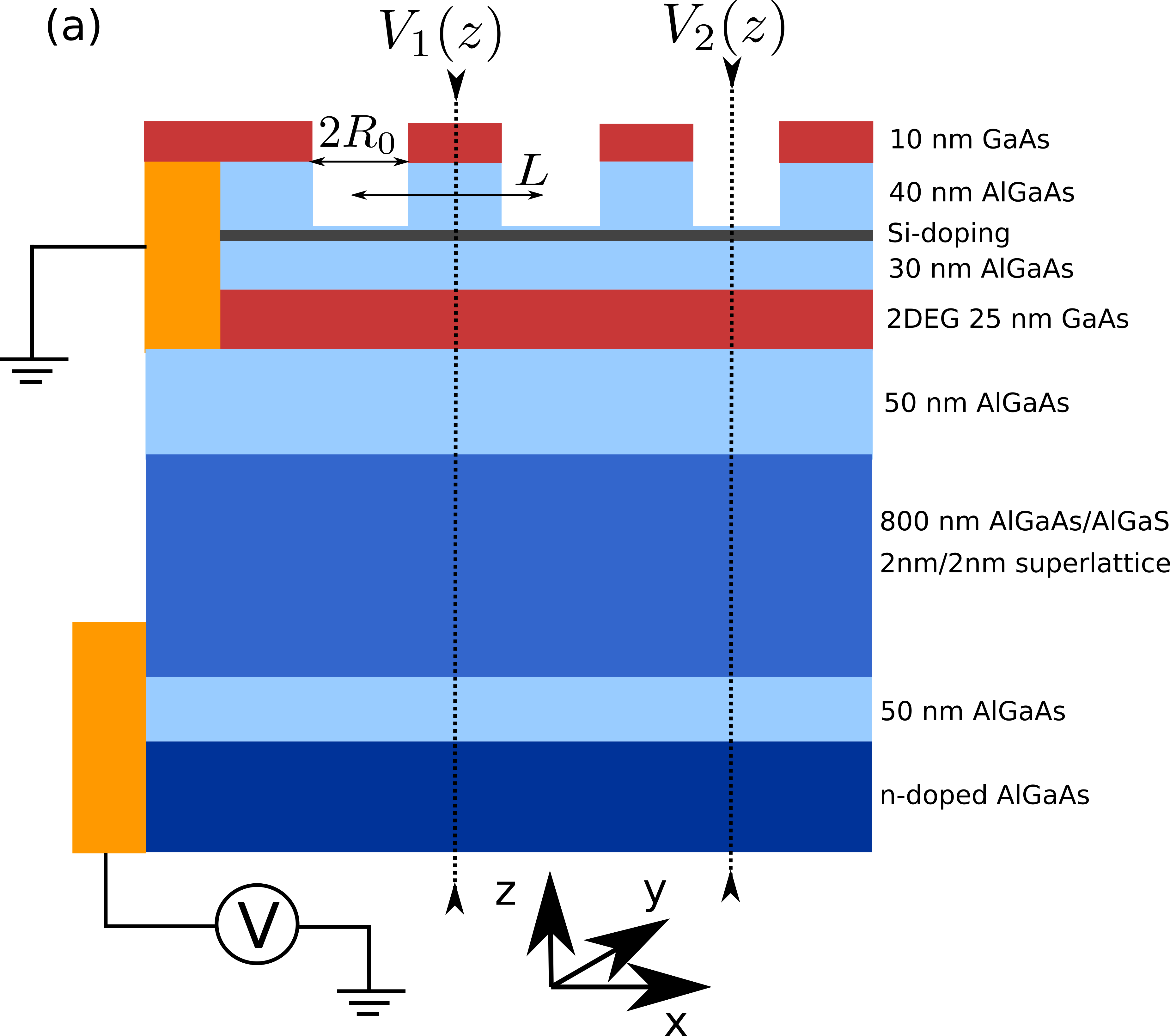
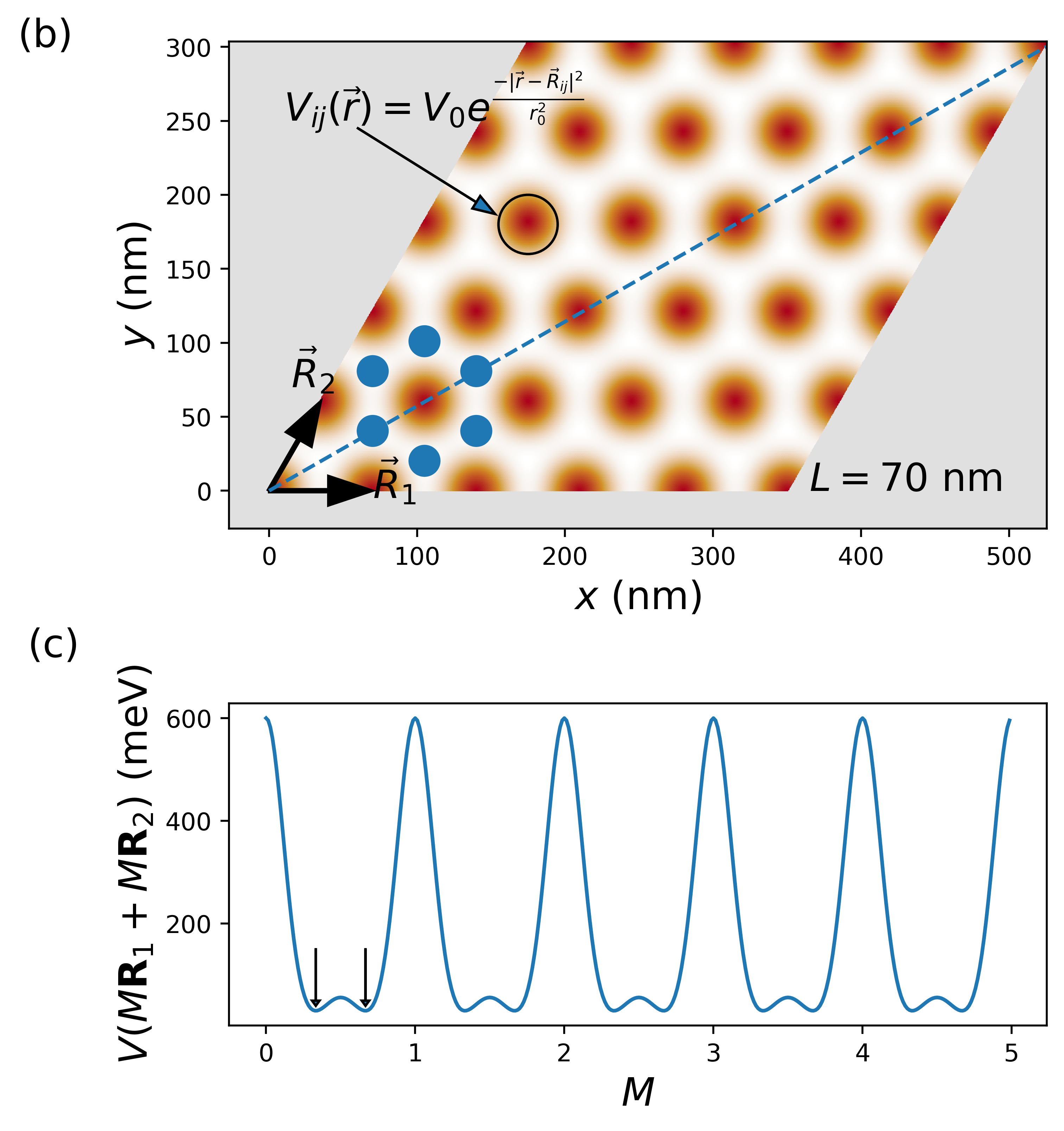
The potential amplitude in Eq. (1) is determined by means of the standard Schrödinger-Poisson approach used separately for two cross sections depicted in Fig. 1(a) by dashed lines. Assuming translation symmetry in the plane, , the Schrödinger equation can be reduced to the 1D form
| (2) |
where , is the effective mass in the direction perpendicular (parallel) to the layers and the potential is the sum of two components: (i) related to the discontinuity of the conduction band at the GaAs/AlGaAs interfaces and (ii) the electrostatic potential that includes the electron-electron interaction and the electric field from the gate. The latter can be determined at the mean-field level from the Poisson equation given by
| (3) |
with the charge density , where is the doping profile and is the electron distribution. The electron density is obtained by
| (4) |
where the factor accounts for the spin degeneracy, is the temperature, is the chemical potential and is the Fermi-Dirac distribution integrated over the and components of the wave vector,
| (5) |
Equations (2) and (3) are solved numerically using the finite difference method with Dirichlet boundary conditions. The existence of 2DEG in the main quantum well results from the Si delta doping located nm above. The value of is chosen to correspond to the electron concentration in 2DEG at the level of , i.e., about two electrons per unit cell, as provided in the experiment Du et al. (2021). Then, for a chosen the self-consistent energy profile is determined for the cross section with the etched region (see Fig. 1(a)) and the potential amplitude is estimated based on the adiabatic approximation according to the formula
| (6) |
where and are energies related to the lowest lying states for the etched and non-etched cases, respectively. The procedure is repeated until self-consistency is reached, which we consider to occur when the potential variation between two consecutive iterations is less than eV. Calculations have been carried out for the material parameters corresponding to GaAs (AlGaAs): GaAs, AlxGa1-xAs, GaAsAlxGa1-xAs, GaAs, AlxGa1-xAs and the conduction band minima , where the energy gap GaAs eV, AlxGa1-xAs. We set and K.
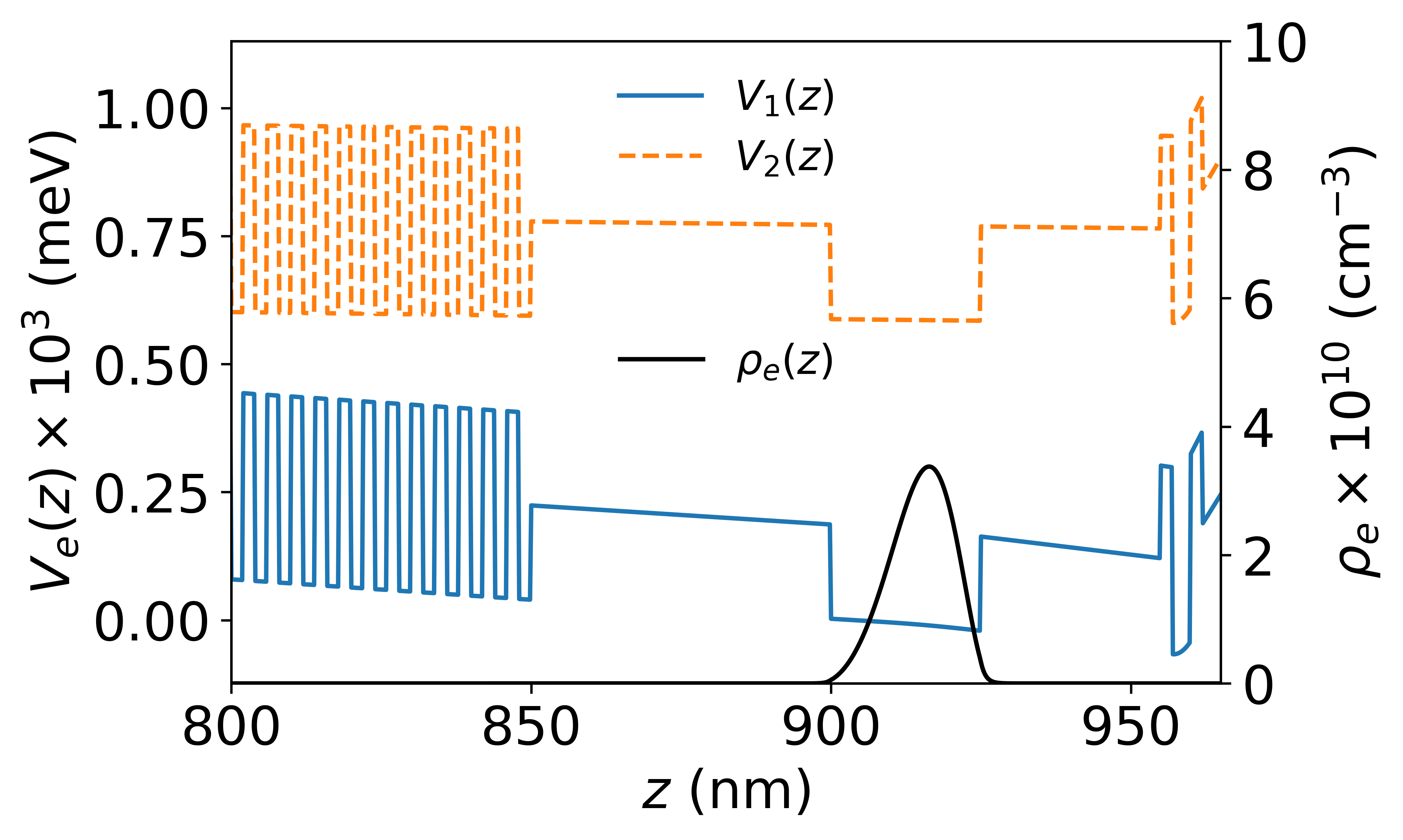
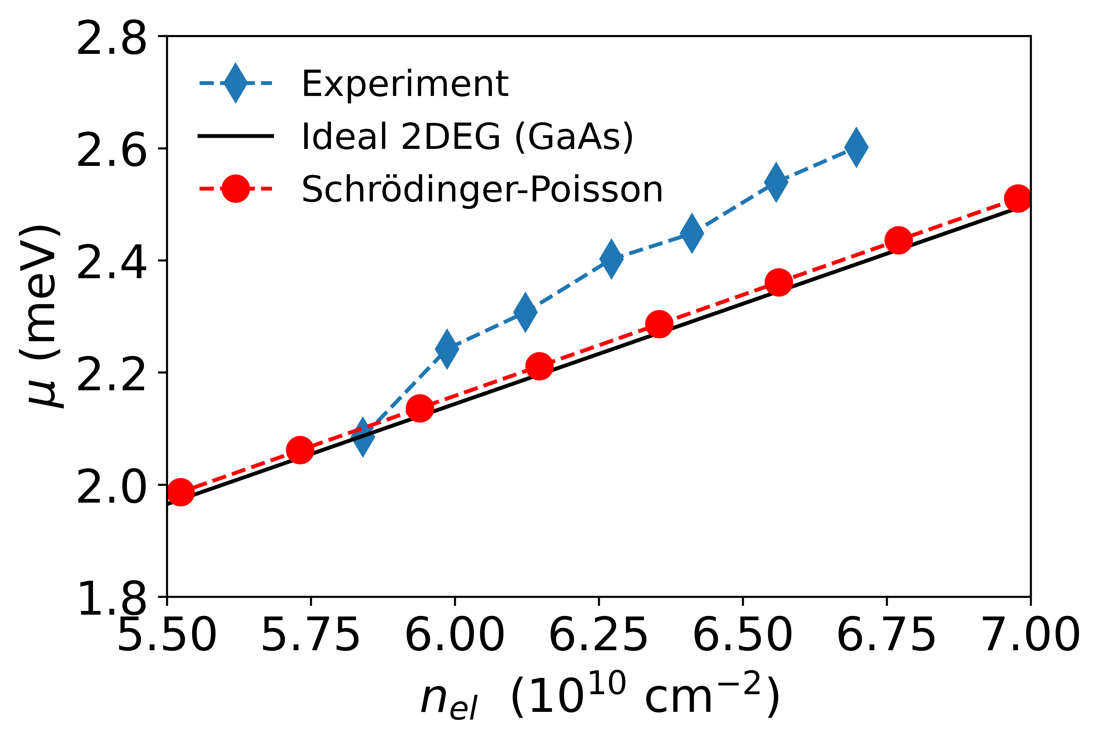
The resulting potential profiles (non-etched case) and (depth of etching nm) are presented in Fig. 2. The local maximum of the AD potential is estimated to be meV according to Eq. 6. We confirm the reliability of our procedure by comparing the calculated Fermi energy as a function of . In Fig. 3 we present obtained for the potential profile , as well as for the available experimental data Du et al. (2021) and the dependence corresponding to the ideal 2DEG model. The Fermi energy for the considered concentration range is meV meV. Remarkably, the energies evaluated within Schrödinger-Poisson scheme are in almost perfect agreement with those obtained for the ideal 2DEG with values only about lower than the experimental ones.
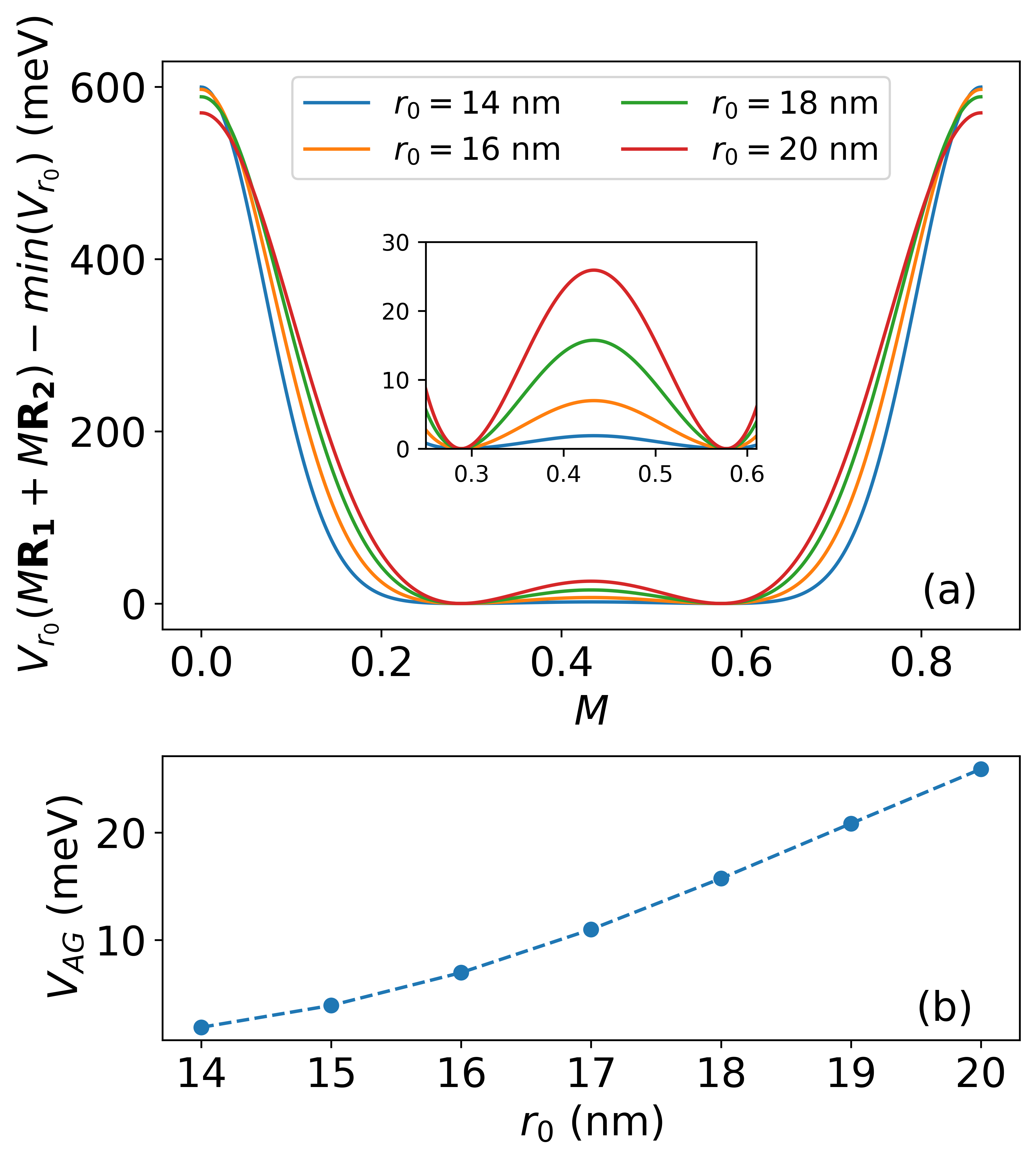
The estimated value of is finally applied to Eq. 1, which defines the planar 2D potential for a given parameter . We focus on AD radii nm nm. These values provide that exposes local maxima at and minima at where and (Fig. 4(a)). In particular, the points defined by the vectors correspond to the honeycomb lattice. The depth of the local minima depends on . For the lower range of considered, is only of the order of a few microelectronvolts, while for nm meV, as derived from the data shown in Fig. 4(b). Thus, it may be expected that a sufficiently large enforces a stronger confinement of electrons and, in turn, their localization in honeycomb trapping centers, which gives the opportunity for emerging strongly correlated state.
II.2 Artificial lattice: Mean-field approach
The elaboration of eventually allows us to perform an analysis of the electronic properties of the formed artificial honeycomb lattice. First, we provide a mean-field approach in which we decouple the modulated 2DEG from the rest of the system. It is done by factorizing a single-electron wave function . Within this assumption, to estimate whether the distribution of electronic density (at a concentration of two electrons per elementary cell) for the estimated potential is honeycomb-like, we solve again the Schrödinger-Poisson problem,this time, in plane for , i.e.,
| (7a) | |||
| (7b) | |||
| (7c) | |||
where is the number of electrons in the unit cell and stands for the spin component. The factor in Eq. 7c refers to mean electron concentration (per spin) with respect to direction in 2DEG. Eventually the estimated total mean field 2D potential at given is modeled as a sum of and resulting from the self-consistent numerical solution of Eqs. 7(a-c), that is,
| (8) |
Eventually, is used to solve the two-dimensional mean field model defined in Eqs. (7a-c). In our calculations we take a single unit cell and assume periodic boundary conditions. A computational procedure is performed on the triangular mesh consisting of nodes. We consider the half-filled case, that is, , where is an area of the unit cell.
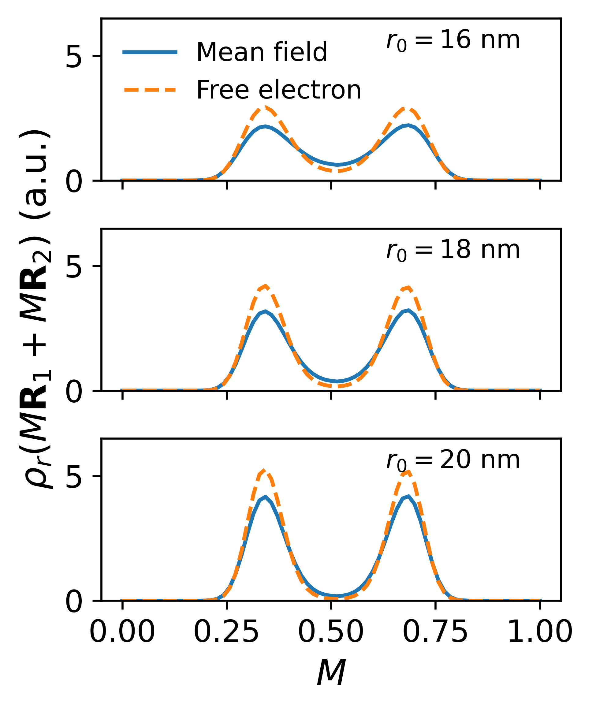
This self-consistent mean-field (MF) approach reveals a meaningful renormalization of the density distribution compared to that of the free electron (non-interacting) case. Namely, the inclusion of Coulomb interactions leads to the more uniform smearing of carriers throughout as can be deduced from Fig. 5. Particularly, this tendency is meaningful for the lower values of , as increases with radius of AD.
III Wannier basis and Single-particle Hamiltonian
The task of constructing the Wannier basis is crucial in view of the reliable determination of both the single-particle Hamiltonian in Tight Binding Approximation (TBA) and the electron-electron interaction amplitudes. In the considered system, the minima of the trapping centers are expected to be shallow, specifically for the semimetallic case, and the distance between the neighboring dots in the honeycomb lattice is . Here, the Wannier functions are obtained by application of the Projection Method Marzari et al. (2012) adapted to a 2D case. This method is based on projecting smooth trial functions centered at positions that are supposed to correspond to the maxima of the electronic density onto Bloch states represented by (where refers to the band index). Subsequently, the procedure that provides unitary transformation is carried out, which eventually results in well-localized Wannier states when are correctly guessed. Namely, we obtain by numerical diagonalization of the single-particle mean-field Hamiltonian defined as
| (9) |
Next, we take the auxiliary basis defined as
| (10) |
where the summation index enumerates the considered bands, to construct the Löwdin-orthonormalized Bloch-like states Marzari et al. (2012)
| (11) |
where . Eventually, Wannier states are obtained by applying the standard Fourier transform, i.e.,
| (12) |
For each considered , the numerical representation of the Hamiltonian given in Eq. 9 is implemented in KWANT package Groth et al. (2014) and diagonalized in the momentum space for the particular wave vector . We probe equally spaced points from the first Brillouin in the unit cell spanned by vectors and that conform to the standard relation . We choose Gaussian trial functions ,
| (13) |
with , where and correspond to two minima present in the confining potential surface at and respectively. Thus, we construct the Wannier basis properly describing the two lowest bands of the system. The presented results correspond to nm, although our test calculations have not revealed any significant differences for , which are and nm. The integration manifold in Eq. 10 has been chosen to be the area corresponding to unit cells to ensure the proper decay of for the assumed value of .
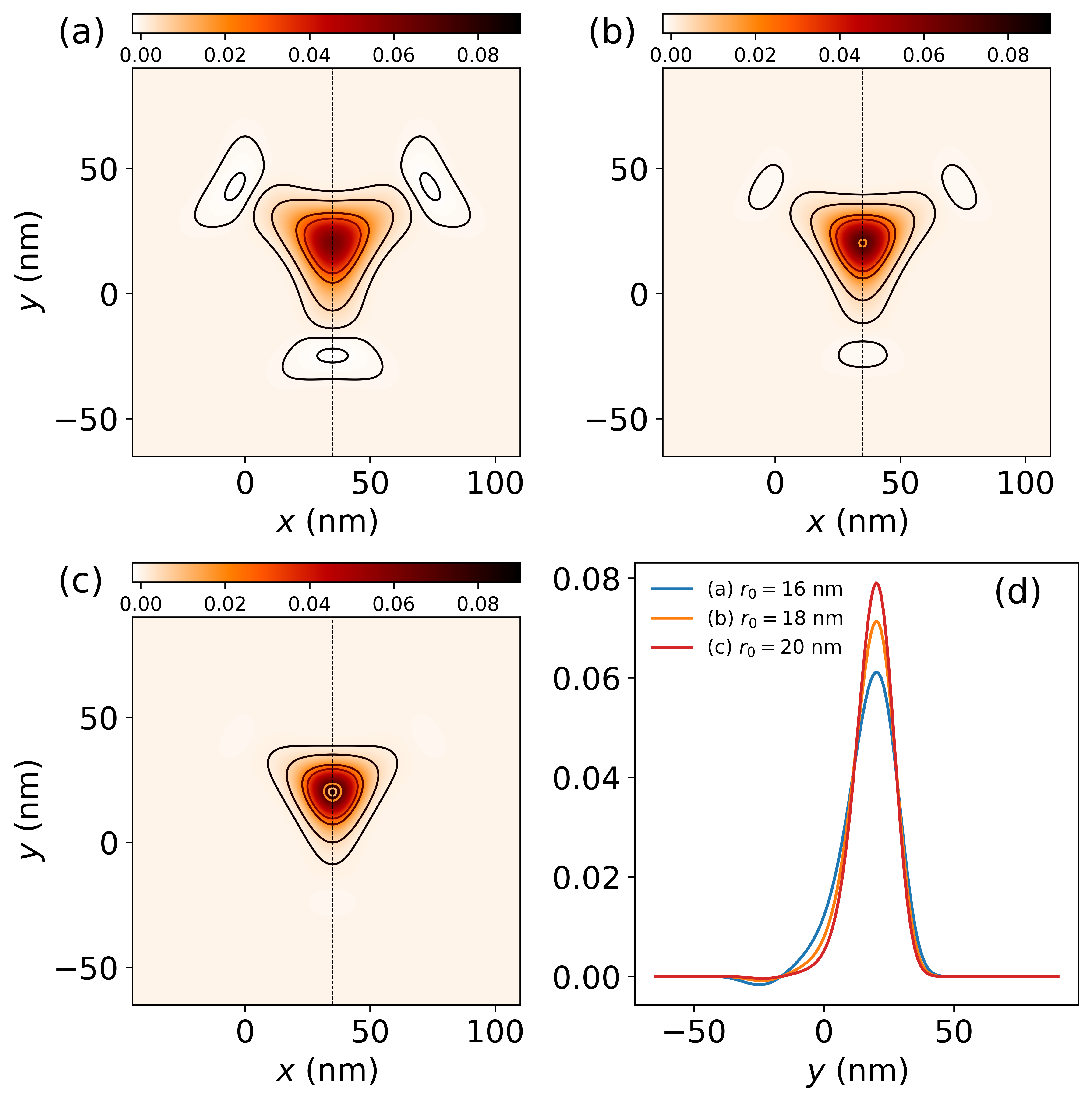
In Fig. 6(a-c) we show representative plots of the Wannier functions for and different values of the parameter . Note that they preserve the three-fold rotational symmetry as desired. The same feature holds for since it is reproducable from by means of the following transformation,
| (14) |
where is the translation by the vector and is operator of reflection with respect to the direction given by . Therefore, we disregard the analysis for the case as the one with is fully representative; however, we emphasize that Eq. 14 holds (within numerical precision) also from the perspective of our numerical calculations. The validity of the procedure has been confirmed by inspecting the orthogonality, which, by construction, should be fulfilled exactly. We have found that this requirement is met within the numerical precision.
From the data contained in Fig. 6 one may conclude that the spatial extent of the resulting Wannier states shrinks with increasing , which can be regarded as a natural consequence of mutual enforcement of trapping. However, since these states are obtained with electron-electron interactions at the level of the mean-field approach, we do not find it trivial, since the confining role of the local minima in is compatible with respect to as comes from Fig. 5. Furthermore, in addition to enhanced localization, the nodal lines that reside in the vicinity of the location of the nearest neighbor (nn) centers and the three local minima enclosed by them disappear for approaching nm.
In the next step, evaluated Wannier functions are subsequently utilized for the construction of TBA Hamiltonian given explicitely in second quantization fromalism as
| (15) |
The in Eq. 15 are defined by relation , where number kind of Wannier function, () creates (annihilates) an electron of spin associated with appropriate , and,
| (16) |
For the sake of clarity, we introduce the following notation,
| (17) |
where maps the pair of position-orbital indices into the proper natural number labeling -th as the nearest neighbor corresponding to the pair .
The notation is completed by assigning
| (18) |
as is the convention commonly used.
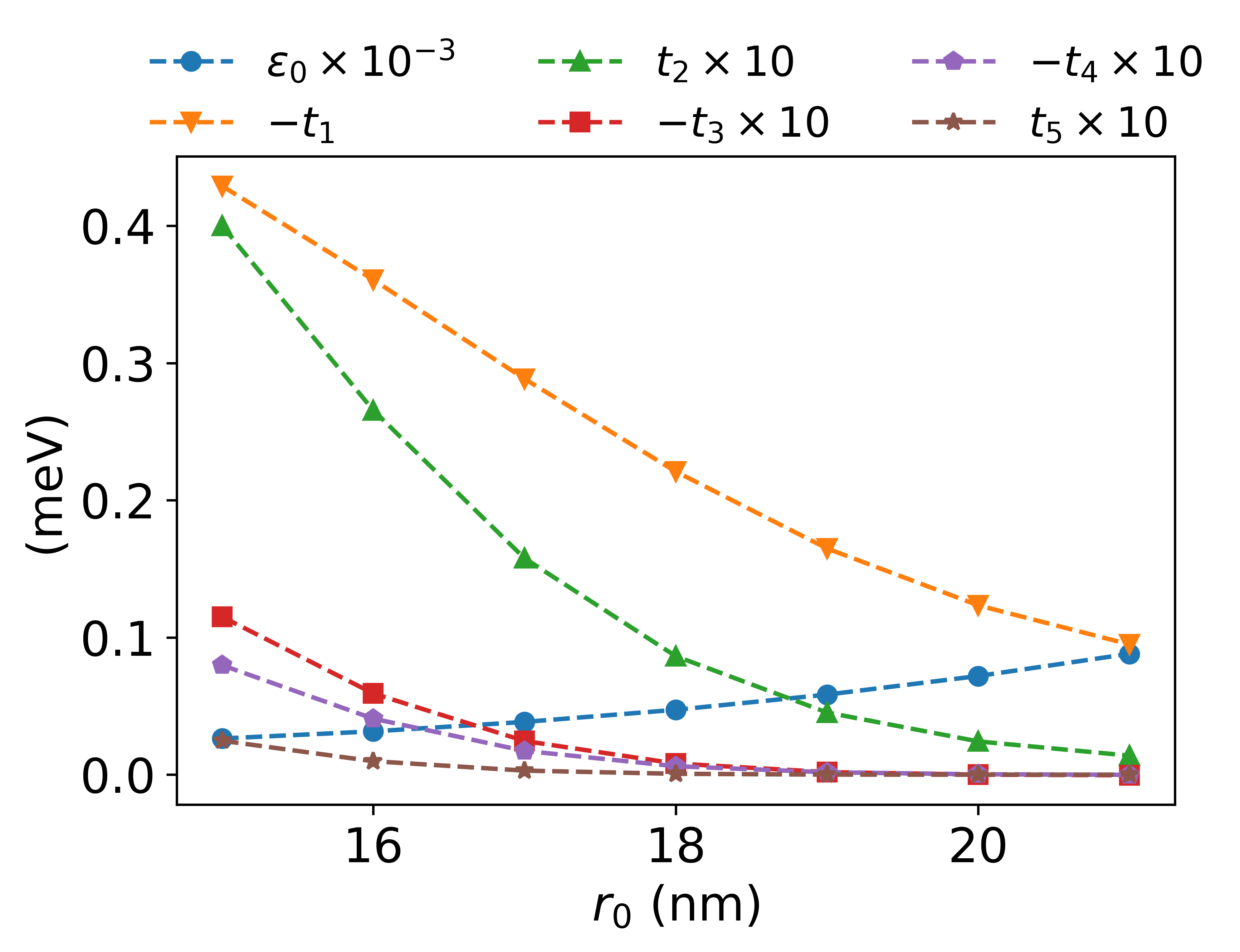
In Fig. 7 we present values of single particle amplitudes up to as a function of . When the size of the trapping center shrinks, the value of increases. The opposite holds for , which is, however, of the order of meV in the entire examined range of . The hopping values are positive and of an order of magnitude lower than . Note that we have computed the hopping integrals up to and found their rapid decay with increasing , that is, meV for each value of .
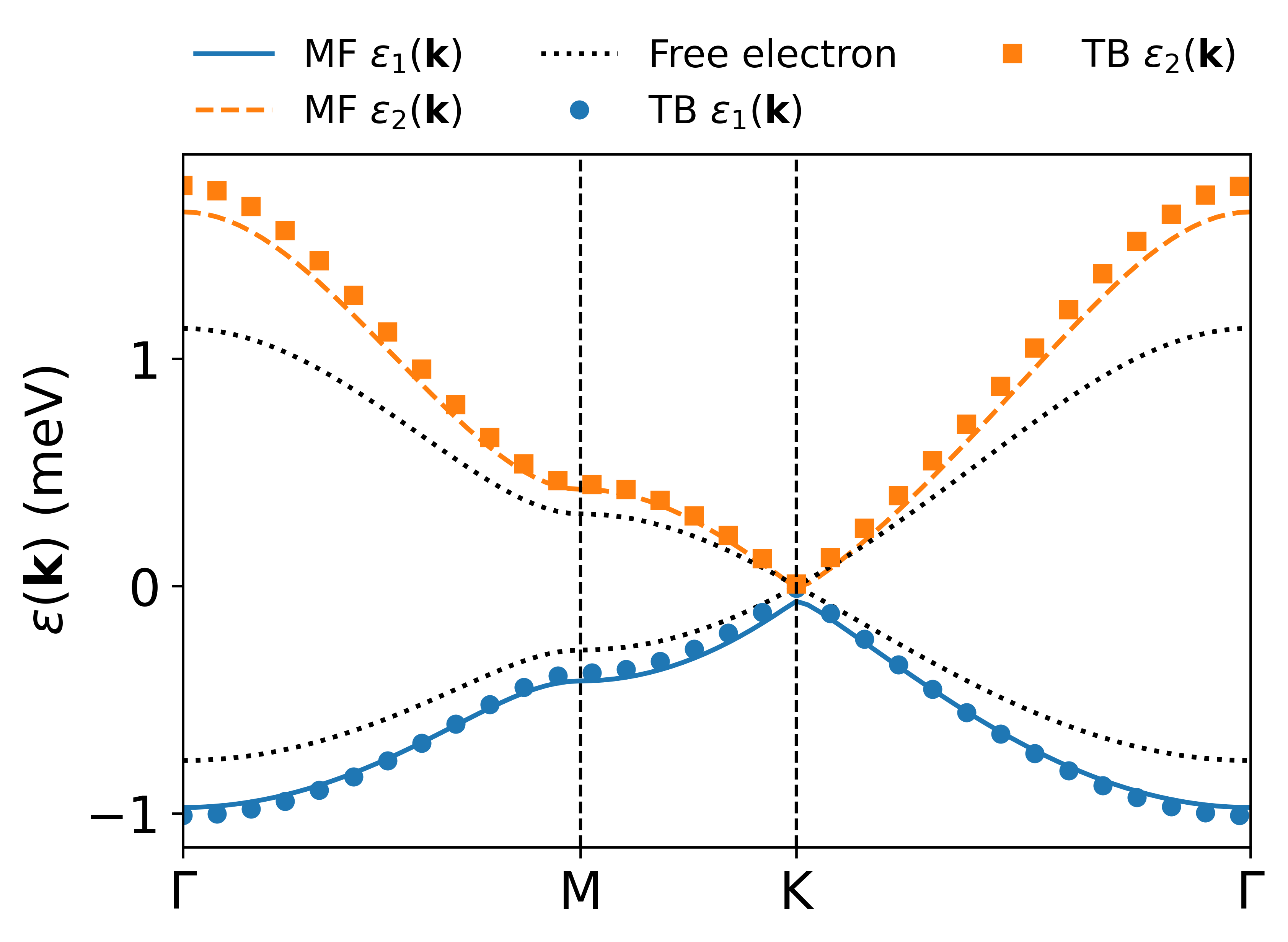
Finally, the obtained sets are utilized to formulate for each value of . In Fig. 8 we present a spectrum for nm that gives which is in good agreement with experimental evidence Du et al. (2021). That is, the formation of the Dirac cone in the vicinity of can be clearly identified. Notably, the difference is of particular interest, since as it can be confronted against the energies of van Hove singularity peaks in the photolouminescence spectra. As comes from Fig. 8, meV is close to the experimental value meV. Namely, resulting from both approaches are nearly identical, which validates the procedure covering Wannier basis elaboration, as well as the subsequent calculation of hopping parameters presented in the further part of the paper.
The dispersion relation obtained by the free electron approach provides a significantly different , which is meV. Also, in this case, both bands are narrower compared to the MF approach. We do not find perfect agreement of meV with respect to the value meV provided by Du et al. However, from the data contained in their work it is difficult to extract the precise value of for carrier concentrations that result in the presence of ALD. Also, since they indicate that the emergence of the honeycomb lattice results from the filling of the lower band, resulting in the occupation of states for which is slightly below , we consider this disagreement to be a minor issue.
Importantly, with increasing we observe a decreasing value of , as well as a narrowing of the entire band structure, reflecting a stronger confinement of electrons in trapping centers. Therefore, it may be expected that at some the enhancement of carrier localization causes electron-electron interactions to dominate over kinetic energy and, consequently, drives the system to the strongly correlated regime. To clarify this presumption, we further study the interaction amplitudes, construct a full electronic Hamiltonian, and find its approximate ground state by means of VMC method for the selected sets of interactions.
IV Interacting picture
IV.1 Electronic interactions and Hamiltonian
The determination of Wannier functions and allows to evaluate the complete electronic Hamiltonian ,
| (19) |
where contains electron-electron interaction terms. Although the finite width of 2DEG affects only by the additive constant (related to confinement in the direction), it is not the case for the interacting part Biborski et al. (2021). Thus, takes the following form
| (20a) | |||
| (20b) | |||
| (20c) | |||
Note, that we take , i.e., the lowest energy state obtained within Schrödinger-Poisson scheme as described in Sec. II A. The electron-electron interaction operator is taken in the Yukawa potential form, to account for the screening effects among electrons in 2DEG (see Section Results), that is,
| (21) |
where is the electron charge and is the estimated length of the Thomas-Fermi wave vector.
Evaluation of microscopic parameters (,) eventually leads to formulation of the Hamiltonian , which can be diagonalized only by approximate methods. Here, we exploit the Variational Monte Carlo technique Biborski et al. (2021) as will be presented at the end of this section.
The leading elements of the electron-electron interaction tensor provided in Eq. 20 can be obtained numerically. However, to perform this task, the length of the Thomas-Fermi wave vector in Eq. 21—which tunes the magnitude of screening—needs to be reasonably estimated.
The screening, directly related to the density of the electron gas, together with the local confinement of the carriers, may play a key role in the tuning of the magnitude of electron-electron interactions Knörzer et al. (2022). In our case, the Wigner-Seitz radius (where stands for dimensionality) at cm-2 is when treating the system as strictly two-dimensional, and when one considers it as quasi-two-dimensional, that is, as being a layer of width nm. Here, both values of are accidentally close to each other. As they are , one concludes that electron-electron interactions and kinetic energy are of similar magnitude Kotov et al. (2012); Ortiz et al. (1999). Thus, disregarding the modulation described by for a while, the system may be safely considered to be the one in which the influence of Coulomb interactions between carriers is moderate with respect to its electronic properties, namely . The system falls into the class of the so-called intermediate regime Ortiz et al. (1999) with respect to the relation between electron-electron interactions and their kinetic energy.
Also, as for nm exhibits only shallow local minima and the resulting density profiles are characterized by the nearly homogeneous distribution of electrons (excluding areas of ADs) with relatively weak local maxima located at honeycomb lattice sites, it seems reasonable to assume metallic-like screening for this case. Therefore, increasing should also affect the screening length. However, assuming its value as that in the non- or weakly confinig regime, one only overestimates the magnitude of and when interactions become significantly greater than hopping amplitudes, one may deduce that the strongly correlated regime is achieved. Therefore, such a strategy provides only an overestimation of the minimal values of for which ALD should exhibit typical phenomena for the strongly correlated system.
We inspect the values of —where is the Thomas–Fermi length, which is supported by the following estimations. First, we may consider the resulting from the ideal 2DEG approach assuming and , that is, the specific values of the effective mass and dielectric constant of the GaAs material, respectively. In this case, since does not depend on the carrier concentration, nm, where is the effective Bohr radius. On the other hand, taking the 3D approach and , one is left with nm, thus a value nearly twice higher than for the 2D case. Eventually, can be estimated on the basis of a quasi-2D model (slab) of 2DEG elaborated by Moreno and Méndez-Moreno Moreno and Méndez-Moreno (2001). Their approach leads to nm for the slab width of nm, i.e. a value substantially lower than that of the ideal two-dimensional electron gas. As the formulation of a general description of screening and its role in a quasi-two-dimensional system is a complex problem that is beyond the scope of this work, we examine the values of , relying on the estimations presented above.
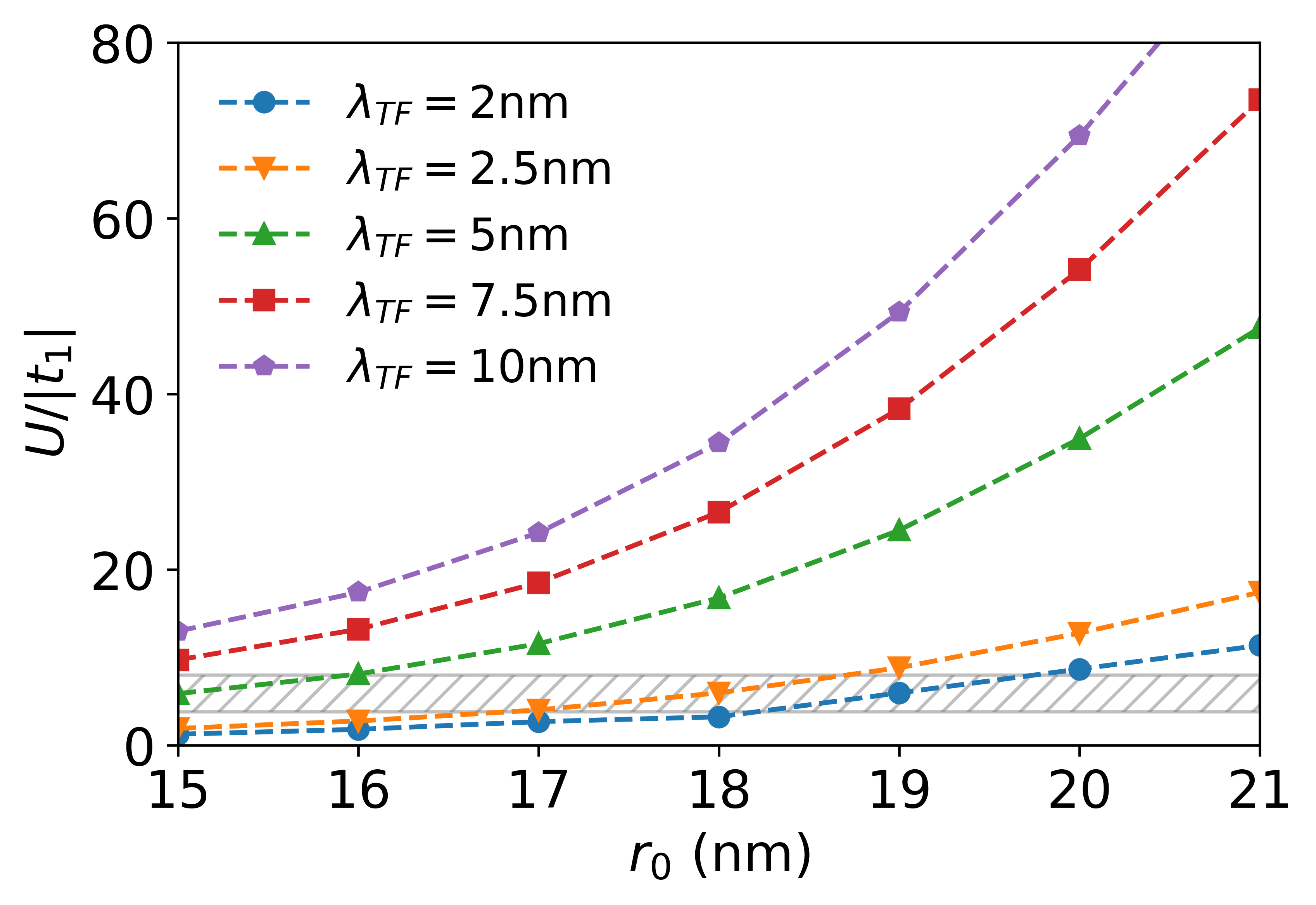
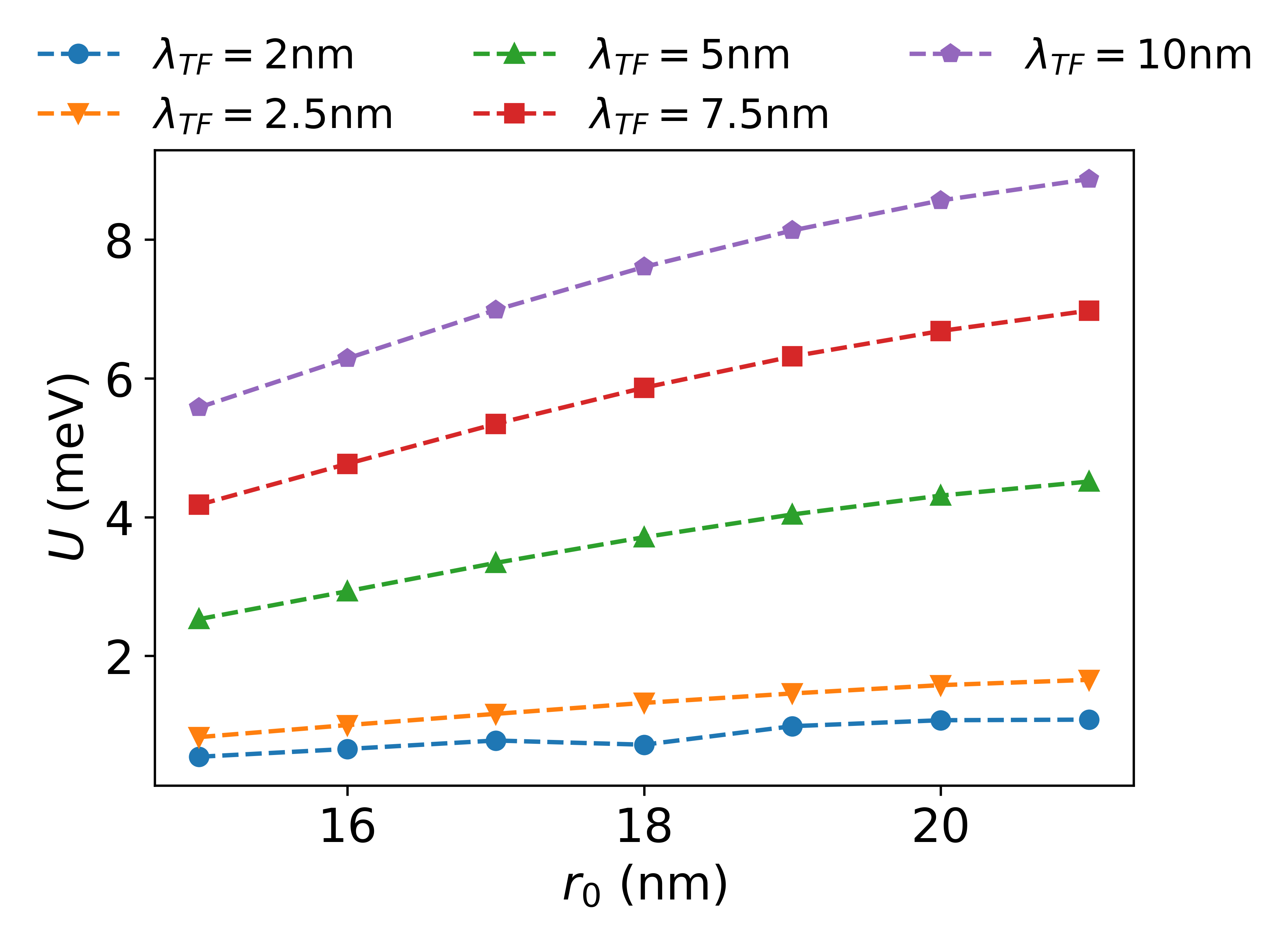
We compute interaction amplitudes of the form , that is, we take into account the on-site Hubbard interaction (applying the same rule of indexing as for hoppings—see Eq. 17), as well as intersite interactions with up to . The calculation procedure has been carried out using the Cuba library Hahn (2005); Biborski et al. (2021) designed for the integration of multi-variable functions. In Fig. 9 we present values of as a function of radius for the selected screening lengths . According to the increasing localization of Wannier functions with , the on-site repulsion amplitudes also increase. For example, for nm and nm meV, while for the same screening length but for nm, we obtain meV. Importantly, for nm, the ratio for nm, as can be seen in Fig. 10, which may suggest that the system is in the vicinity of the transition point between the semi-metallic and antiferromagnetic Mott insulator (AFMI) phases Sorella et al. (2012). However, since we identify the radius as the one that corresponds to the experimental setup for which there is no evidence of AFMI formation Du et al. (2021), we conclude that should be considered as nm in the framework of the elaborated model.
Note that since is one order of magnitude greater than for the entire range of , the estimate of critical radius for which AFMI possibly emerges by inspecting is justified, since in this view the electronic properties of the system should be similar to those of the Hubbard model on the honeycomb lattice. Thus, taking nm, we find that the transition should occur at nm.
Next, we examine the intersite amplitudes . We find that for nm, they are at least two orders of magnitude smaller than the corresponding for each considered . Therefore, the interplay between is unlike to cause the formation of a charge density wave (CDW), which is believed to compete with the semimetallic and AFMI phases when the magnitude of intersite interactions is significant Wu and Tremblay (2014). Eventually, according to the values of the dominating interaction amplitudes, we expect a transition between the semi-metallic and AFMI phases when the value of increases. We illustrate this trend by the results obtained from our VMC calculations for nm as presented below.
IV.2 Ground state of interacting Hamiltonian by means of VMC method
We formulate a minimalistic model for the interacting electrons on honeycomb lattice described by the Hubbard Hamiltonian with hoppings extending up to the nn. Namely, we take into account only the on-site interactions, as the inter-site interactions are—as mentioned—at least of two orders of magnitude weaker. Calculations have been carried out for the lattice consisting of unit cells, that is, for sites within imposed periodic boundary conditions. The simulations have been carried out using the mVMC software Misawa et al. (2019) with the help of self-elaborated, re-usable and generic Hamiltonian input generator Biborski (2023). The trial state is in Pfaffian form, i.e. product of antiparallel spin pairing terms, supplied with the on-site Gutzwiller and inter-site long-range Jastrow projectors, which are responsible for capturing the electronic correlation effects Biborski et al. (2021). Variational parameters corresponding to pairings, Gutzwiller and Jastrow projectors are chosen with periodicity defined by a supercell consisting of unit cells. According to the spin polarization of the system, we impose the constraint , that is, the total component of the spin is zero.
In the following, we present the calculations obtained for nm, emphasizing that it can be regarded as overestimated for the strongly confined regime. However, as will become clear, it allows us to reveal typical features of the strongly correlated system when nm.
First, we analyze the average double occupancy defined as
| (22) |
where is the particle number operator associated with the site labeled by and is the spin component of the electron that resides at the site .
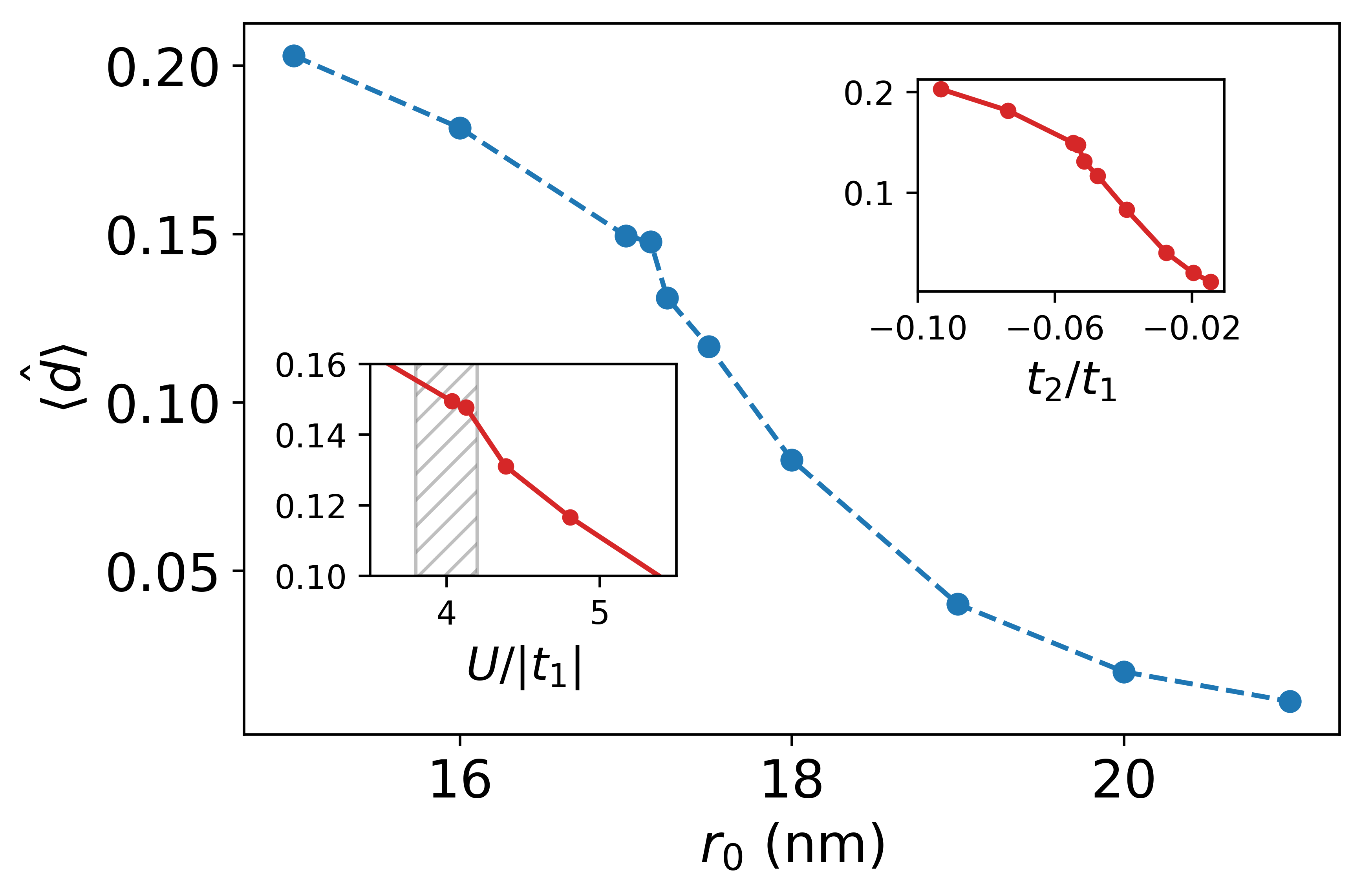
In Fig. 11 we show as a function of . Its value decreases with an increasing AD radius. This behavior is driven by the mutual enhancement of , as well as the narrowing of the occupied band. We performed auxiliary calculations for and nm to identify an abrupt drop in in vicinity of nm, which is the characteristic indicator of transition to the insulating state driven by electronic correlations.
The emergence of AFMI state is also supported by the analysis of the spin-spin correlation functions. Namely, we investigate the AF spin order parameter provided by Sorella et al. Sorella et al. (2012), but defined for the -component of , i.e.,
| (23) |
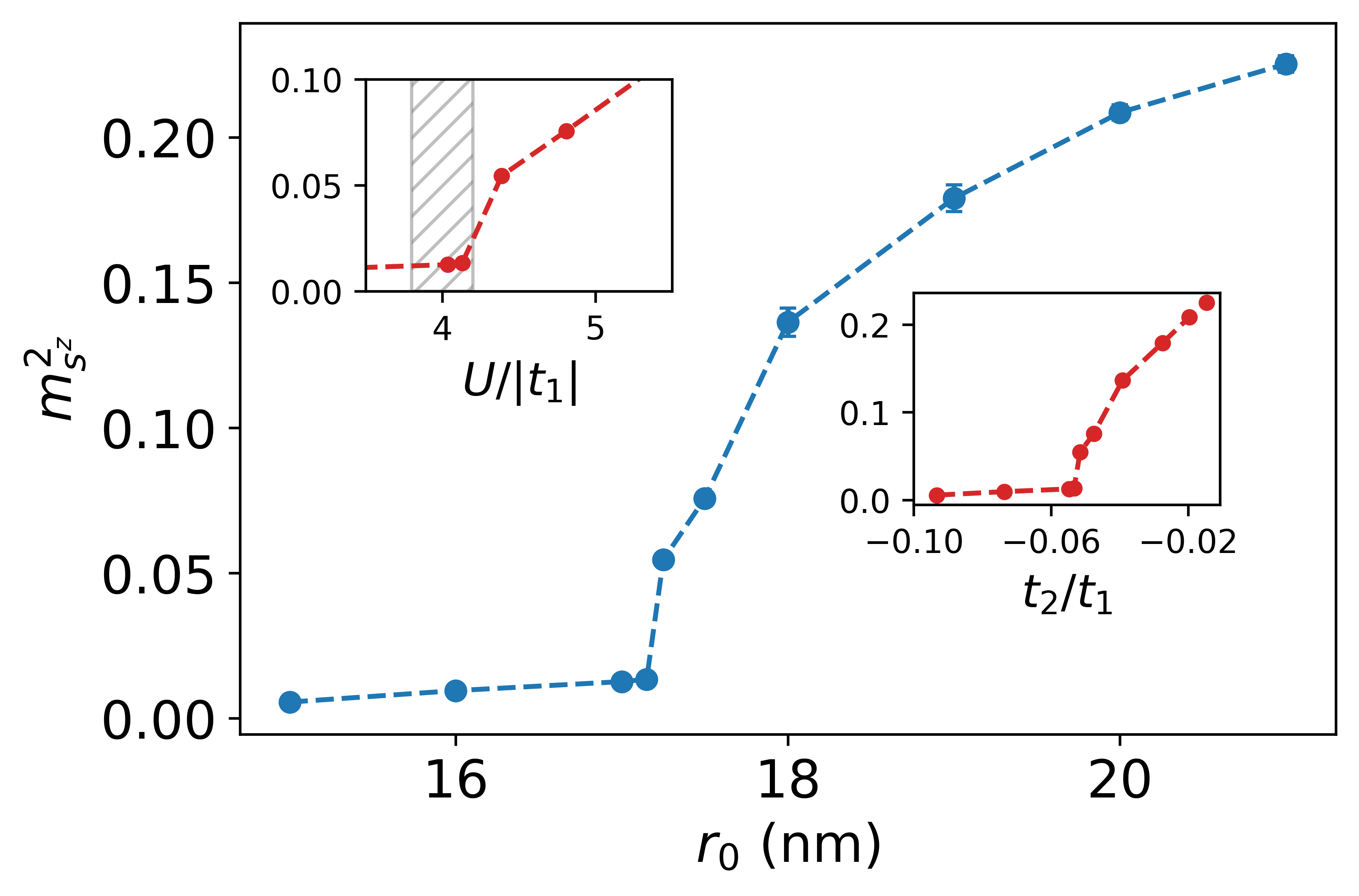
In Fig. 12 we present analogously to the double occupancies shown in Fig. 11. It is clearly visible that the AF order for nm is marginal since . However, for nm, we observe its radical increase, namely, for nm, which is the next case considered, it is .
Recapitulating, when is translated into the ratio (see the insets in Figs. 11, 12), simultaneous, anomal behaviour of both and can be observed for nm. These values of correspond to , the range which nearly overlap with , i.e., critical values for which transition to AFMI takes place, as it has been estimated in the framework of Quantum Monte-Carlo approaches Sorella et al. (2012); Meng et al. (2010); Raczkowski et al. (2020).
V Summary and conclusions
In this paper, we studied the anti-dot honeycomb lattice model in view of the importance of electron-electron interactions. Within the assumed form of the quantum dot potential and the multilevel computational scheme, we provided evidence of the possibility of the formation of an antiferromagnetic Mott insulator. Our modeling scheme reveals that the radius of the antidot is crucial in this context. In addition, the inclusion of metallic screening among electrons seems to be essential for the strength of the electron-electron interactions, specifically when the radius of the antidot is small. Note that we did not have to take into account the screening of the metallic gates that induce the periodic potential Knörzer et al. (2022); Biborski et al. (2021); Byrnes et al. (2008) as the honeycomb structure here results from the triangular etching pattern of the upper layers. Also, we do not take into account any kind of scattering centers, such as ionic impurities or any other kind of disorder in the system. Therefore, the whole screening considered here has its origin in the metallic nature of 2DEGs Kollar and Sachdev (2002). In this spirit our supporting VMC analysis reveals possible mapping of interacting electrons in AD honeycomb lattice to the Hubbard model. Our study provides a straightforward way to exploit the devices that are currently fabricated for the realization of strongly correlated artificial Dirac systems. The experimental confirmation of our predictions would open up the opportunity for a better understanding of the electronic properties of graphene-like systems in a controllable manner. Moreover, we indicate that in addition to the correlation effects studied here, the AD honeycomb lattice formed in 2DEG may also serve as a simulation platform for strain-induced opening of the gap in honeycomb systems Cocco et al. (2010); Rut et al. (2023), since strain can be emulated by the distorted QD assembly. Thus, the proposed modeling scheme may also be considered useful from this point of view.
VI Acknowledgement
This work was supported by National Science Centre (NCN) agreement number UMO-2020/38/E/ST3/00418.
References
- Kotov et al. (2012) V. N. Kotov, B. Uchoa, V. M. Pereira, F. Guinea, and A. H. Castro Neto, Rev. Mod. Phys. 84, 1067 (2012).
- Tang et al. (2018) H.-K. Tang, J. N. Leaw, J. N. B. Rodrigues, I. F. Herbut, P. Sengupta, F. F. Assaad, and S. Adam, Science 361, 570 (2018), https://www.science.org/doi/pdf/10.1126/science.aao2934 .
- Das Sarma et al. (2007) S. Das Sarma, E. H. Hwang, and W.-K. Tse, Phys. Rev. B 75, 121406 (2007).
- Wu and Tremblay (2014) W. Wu and A.-M. S. Tremblay, Phys. Rev. B 89, 205128 (2014).
- Assaad and Herbut (2013) F. F. Assaad and I. F. Herbut, Phys. Rev. X 3, 031010 (2013).
- Sorella et al. (2012) S. Sorella, Y. Otsuka, and S. Yunoki, Scientific Reports 2, 992 (2012).
- Meng et al. (2010) Z. Y. Meng, T. C. Lang, S. Wessel, F. F. Assaad, and A. Muramatsu, Nature 464, 847 (2010).
- Raczkowski et al. (2020) M. Raczkowski, R. Peters, T. T. Phùng, N. Takemori, F. F. Assaad, A. Honecker, and J. Vahedi, Phys. Rev. B 101, 125103 (2020).
- Otsuka et al. (2016) Y. Otsuka, S. Yunoki, and S. Sorella, Phys. Rev. X 6, 011029 (2016).
- Liebsch and Wu (2013) A. Liebsch and W. Wu, Phys. Rev. B 87, 205127 (2013).
- Arya et al. (2015) S. Arya, P. V. Sriluckshmy, S. R. Hassan, and A.-M. S. Tremblay, Phys. Rev. B 92, 045111 (2015).
- Saleem et al. (2022) Y. Saleem, A. Dusko, M. Cygorek, M. Korkusinski, and P. Hawrylak, Phys. Rev. B 105, 205105 (2022).
- Du et al. (2021) L. Du, Z. Liu, S. J. Wind, V. Pellegrini, K. W. West, S. Fallahi, L. N. Pfeiffer, M. J. Manfra, and A. Pinczuk, Phys. Rev. Lett. 126, 106402 (2021).
- Kylänpää et al. (2016) I. Kylänpää, F. Berardi, E. Räsänen, P. García-González, C. A. Rozzi, and A. Rubio, New J. Phys. 18 (2016), 10.1088/1367-2630/18/8/083014.
- Li et al. (2020) T. Li, J. Ingham, and H. D. Scammell, Phys. Rev. Res. 2, 043155 (2020).
- Räsänen et al. (2012) E. Räsänen, C. A. Rozzi, S. Pittalis, and G. Vignale, Phys. Rev. Lett. 108, 246803 (2012).
- Krix et al. (2022) Z. E. Krix, H. D. Scammell, and O. P. Sushkov, Phys. Rev. B 105, 075120 (2022).
- Li et al. (2017) Y.-M. Li, X. Zhou, Y.-Y. Zhang, D. Zhang, and K. Chang, Phys. Rev. B 96, 035406 (2017).
- Tkachenko et al. (2015) O. A. Tkachenko, V. A. Tkachenko, I. S. Terekhov, and O. P. Sushkov, 2D Materials 2, 014010 (2015).
- Bednarek et al. (2003) S. Bednarek, B. Szafran, K. Lis, and J. Adamowski, Phys. Rev. B 68, 155333 (2003).
- Ciurla et al. (2002) M. Ciurla, J. Adamowski, B. Szafran, and S. Bednarek, Physica E Low Dimens. Syst. Nanostruct. 15, 261 (2002).
- Note (1) Note that we excluded the bottom layer of -doped AlGaAs as detailed information regarding the character of doping has not been provided Du et al. (2021).
- Marzari et al. (2012) N. Marzari, A. A. Mostofi, J. R. Yates, I. Souza, and D. Vanderbilt, Rev. Mod. Phys. 84, 1419 (2012).
- Groth et al. (2014) C. W. Groth, M. Wimmer, A. R. Akhmerov, and X. Waintal, New J. Phys. 16, 063065 (2014).
- Biborski et al. (2021) A. Biborski, M. P. Nowak, and M. Zegrodnik, Phys. Rev. B 104, 245430 (2021).
- Knörzer et al. (2022) J. Knörzer, C. J. van Diepen, T.-K. Hsiao, G. Giedke, U. Mukhopadhyay, C. Reichl, W. Wegscheider, J. I. Cirac, and L. M. K. Vandersypen, Phys. Rev. Res. 4, 033043 (2022).
- Ortiz et al. (1999) G. Ortiz, M. Harris, and P. Ballone, Phys. Rev. Lett. 82, 5317 (1999).
- Moreno and Méndez-Moreno (2001) M. Moreno and R. M. Méndez-Moreno, International Journal of Quantum Chemistry 82, 269 (2001), https://onlinelibrary.wiley.com/doi/pdf/10.1002/qua.1049 .
- Hahn (2005) T. Hahn, Comput. Phys. Commun. 168, 78 (2005).
- Misawa et al. (2019) T. Misawa, S. Morita, K. Yoshimi, M. Kawamura, Y. Motoyama, K. Ido, T. Ohgoe, M. Imada, and T. Kato, Comput. Phys. Commun. 235, 447 (2019).
- Biborski (2023) A. Biborski, (2023), 10.5281/zenodo.8172389.
- Byrnes et al. (2008) T. Byrnes, N. Y. Kim, K. Kusudo, and Y. Yamamoto, Phys. Rev. B 78, 075320 (2008).
- Kollar and Sachdev (2002) M. Kollar and S. Sachdev, Phys. Rev. B 65, 121304 (2002).
- Cocco et al. (2010) G. Cocco, E. Cadelano, and L. Colombo, Phys. Rev. B 81, 241412 (2010).
- Rut et al. (2023) G. Rut, M. Fidrysiak, D. Goc-Jagło, and A. Rycerz, International Journal of Molecular Sciences 24 (2023), 10.3390/ijms24021509.