Nanoscale domain engineering in SrRuO3 thin films
Abstract - We investigate nanoscale domain engineering via epitaxial coupling in a set of SrRuO3/PbTiO3/SrRuO3 heterostructures epitaxially grown on (110)o-oriented DyScO3 substrates. The SrRuO3 layer thickness is kept at 55 unit cells, whereas the PbTiO3 layer is grown to thicknesses of 23, 45 and 90 unit cells. Through a combination of atomic force microscopy, x-ray diffraction and high resolution scanning transmission electron microscopy studies, we find that above a certain critical thickness of the ferroelectric layer, the large structural distortions associated with the ferroelastic domains propagate through the top SrRuO3 layer, locally modifying the orientation of the orthorhombic SrRuO3 and creating a modulated structure that extends beyond the ferroelectric layer boundaries.
I Introduction
Ferroelectric polarisation can be used to affect the properties of other materials. This is well know in ferroelectric field-effect transistors for example, where the polarisation surface charge of the ferroelectric film is used to reversibly dope the adjacent layer, as demonstrated in epitaxial oxide thin film heterostructures Ahn-Science-1995 .
In this work, a PbTiO3 layer is sandwiched between two SrRuO3 layers. In bulk, SrRuO3 is a ferromagnetic metallic transition-metal oxide and is often used as an electrode in the ferroelectric oxides community Eom-Science-1992 . It is also an itinerant ferromagnet with a Curie temperature = 160 K Cao-PRB-1997 . In thin films of this material, the formation of complex spin textures can be induced by the ferroelectric polarisation in an adjacent ferroelectric layer. These include ferroelectric proximity effect near the BaTiO3/SrRuO3 interface giving rise to an emergent Dzyaloshinskii–Moriya interaction, thereby creating robust magnetic skyrmions Wang-NatMat-2018 . Most recently, in SrRuO3/PbTiO3 heterostructures a ferroelectrically induced magnetic spin crystal was observed Seddon-NatCom-2021 .
SrRuO3 is not only affected by the polarisation in adjacent layers, but also by the epitaxial strain imposed by the substrate Koster-RevModPhys-2012 . When grown on SrTiO3, epitaxial SrRuO3 layers are organized into structural domains, according to six possible orientations of the orthorhombic unit cell with respect to the cubic substrate. The orientation of the orthorhombic unit cell and resulting domains is affected by the steps and terraces at the surface of the SrTiO3 substrate Jiang-MSEB-1998 . The growth of SrRuO3 onto vicinal planes of miscut SrTiO3 substrates leads to the privileged development of a majority single domain orientation in which small domains with different orientations are embedded Jiang-APL-1998 . Additionally, control of the SrRuO3 can be achieved not only through the choice of substrate Vailionis-APL-2008 , but also by modifying the growth temperature Zakharov-JMT-1999 . Further structural domain engineering has been conducted through control of substrate miscut direction, demonstrating a one-to-one correspondence between structural domains and magnetic domains Wang-NPJQuantMats-2020 .
A structural coupling can also be achieved by strain propagation between the different layers themselves. As was shown in PbTiO3/SrTiO3/PbTiO3 heterostructures on GdScO3 where the structural coupling between the PbTiO3 and SrTiO3 layers resulted in periodic polar waves in the SrTiO3 Tang-NanoLetters-2021 , in SrRuO3/PbTiO3 superlattices the large local deformations of the ferroelectric lattice are accommodated by periodic lattice modulations of the metallic SrRuO3 layers with very large curvatures Hadjimichael-NatMat-2021 .
At the core of the heterostructure studied here is PbTiO3, a tetragonal ferroelectric with a polarisation developing along the -axis mostly due to ionic displacements. In PbTiO3 thin films, the orientation of the polarisation and arrangement into domain structures have been theoretically studied Pertsev-PRL-1998 ; Pertsev-PRL-2000 ; Koukhar-PRB-2001 ; Li-APL-2001 ; Jiang-PRB-2014 ; Chapman-PCCP-2017 , and are described by phase diagrams with regions of different domain configurations as a function of epitaxial strain and temperature (see review by Schlom et al. Schlom-AnnuRevMaterRes-2007 ). The domain pattern is also affected by the film thickness Kittel-PR-1946 and electrostatic boundary conditions Lichtensteiger-NanoLett-2014 ; Lichtensteiger-NJP-2016 . Complex polarisation configurations in PbTiO3 have been reported recently in PbTiO3/SrTiO3 superlattices Yadav2016 ; Stoica2019 ; Hadjimichael-PhD-2019 ; Hadjimichael-NatMat-2021 ; Goncalves2019 ; Das2019 ; Wang-NatureMaterials-2020 , with simultaneous control of these configurations using electric fields and light, giving rise to novel phenomena like negative capacitance Iniguez-NatureReviewsMaterials-2019 . When grown on DyScO3, PbTiO3 takes the phase, where the polarisation forms ordered ferroelastic domains ( twins), resulting in distortions of the film surface visible by atomic force microscopy Vlooswijk-APL-2007 ; Catalan-NatMat-2011 ; Nesterov-APL-2013 ; Lichtensteiger-APLMaterials-2023 .
Whether through ferroelectric polarisation or strain effects, controlling the structure and morphology of the SrRuO3 thin films is of importance as it will affect the film electronic resistivity via structural and electronic coupling. Here, we study the structural coupling between oxide thin film layers on a set of SrRuO3/PbTiO3/SrRuO3 heterostructures epitaxially grown on (110)o-oriented DyScO3 substrates. We establish the direct role that the ferroelastic domain structure in PbTiO3 plays in the determination of the orthorhombic domain structure in SrRuO3.
II Results
A series of samples was grown by off-axis RF magnetron sputtering on (110)o-oriented DyScO3 substrates, with bottom and top SrRuO3 electrodes of 55 unit cells (u.c.) and PbTiO3 film thickness of 23, 45 and 90 u.c. (see Section. IV.1 for details of samples growth).
The substrate, DyScO3, is orthorhombic with room temperature lattice parameters (in space group) = 5.443(2) Å, = 5.717(2) Å and = 7.901(2) Å Velickov-ZKristallogr-2007 . It is often useful to refer also to the pseudocubic unit cell, where the lattice parameters can be calculated as = = = 3.947 Å, = = 3.951 Å, ==90∘, =2 ()=87.187∘ at room temperature. Here, “” subscript refers to the pseudocubic unit cell, while “” is used to refer to the orthorhombic unit cell. For (110)o-oriented DyScO3, the out-of-plane [001]pc direction is equivalent to [110]o, while the in-plane directions [100]pc and [010]pc are equivalent to [10]o and [001]o respectively (see Supplementary Materials, Figure S1).
The bottom and top electrode, SrRuO3, is orthorhombic with bulk room temperature lattice parameters (in space group) = 5.57 Å, = 5.53 Å and = 7.85 Å Randall-JACS-1959 , corresponding to the pseudocubic unit cell parameters = = 3.924 Å, = 3.925 Å, ==90∘, = 90.413∘. According to the Glazer notation, octahedral tilting in orthorhombic SrRuO3 is described by , implying that RuO6 octahedra are rotated in opposite directions by equivalent magnitude along and (out-of-phase) and in the same direction about (in-phase) Glazer1972 ; Woodward-ActaCrystallographicaB-1997 . On (110)o-oriented DyScO3 substrate, SrRuO3 can grow with different possible orientations Jiang-MSEB-1998 ; Wang-NPJQuantMats-2020 , as described in Figure 1, and Supplementary Materials Figure S1 and S2.
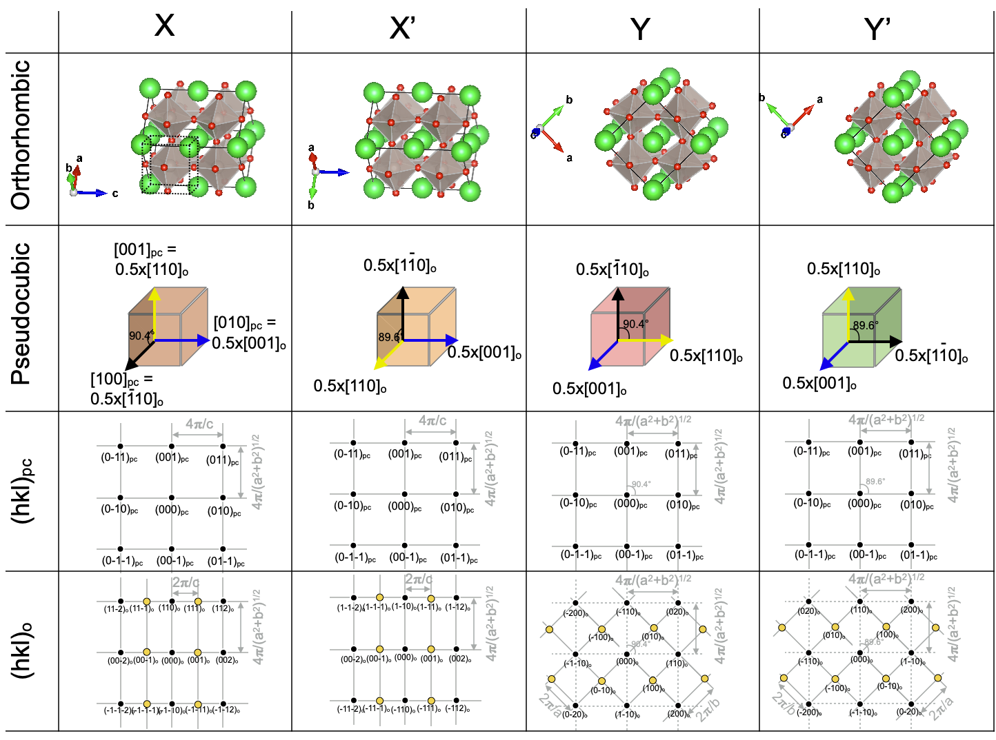
Last, the PbTiO3 is ferroelectric below a bulk critical temperature of 765K with a tetragonal structure, and lattice parameters = = 3.904 Å and = 4.152 Å at room temperature. The in-plane strain imposed by DyScO3 on PbTiO3 films can thus be calculated as along and along , where is the extrapolated lattice parameter of PbTiO3 in the room-temperature cubic paraelectric phase, = 3.957 Å for PbTiO3. To accommodate this strain111Although the strain with respect to is compressive, the system is usually referred to as being under tensile strain because the lattice parameter of DyScO3 is larger than the bulk = axes of PbTiO3., PbTiO3 thin films on DyScO3 at room temperature are expected to be in the -phase, with regions where the -axis points out-of-plane (-domains) as well as regions where it points in-plane (-domains), giving rise to a ferroelastic -domain configuration with 90∘ domain walls. The latter are parallel to the crystallographic planes, and thus are inclined at about 45∘ with respect to the film/substrate interface, as predicted in Ref. Koukhar-PRB-2001 and demonstrated experimentally (see for example Ref. Catalan-NatMat-2011 ; Nesterov-APL-2013 ; Highland-APL-2014 ). Additionally to these ferroelastic domains, the electrostatic boundary conditions and depolarisation field arising from an incomplete screening of the surface bound charges can lead the -domains to alternate between “up” () and “down” () orientations. Although the surface bound charges of our PbTiO3 films are screened by the top and bottom SrRuO3 electrodes, this screening is incomplete Junquera-NAT-2003 ; Aguado-Puente-PRL-2008 ; Stengel-NatMat-2009 ; Li-APL-2017 ; Hadjimichael-PRM-2020 and the depolarisation field still plays a role. Such a combination of mechanical and electrostatic constraints can then result in flux-closure structures, as observed in strained PbTiO3 thin films Tang-Science-2015 ; Li-APL-2017 ; Li-ActaMat-2019 ; Lichtensteiger-APLMaterials-2023 .
II.1 Topographic modulation observed at the heterostructure surface using atomic force microscopy
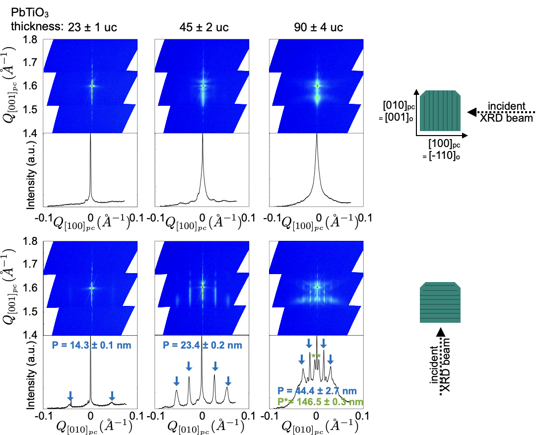
Figure 2(a) shows atomic force microscopy (AFM) images for the three SrRuO3/PbTiO3/SrRuO3 heterostructures grown on DyScO3. The AFM topography images reveal that as the PbTiO3 layer thickness increases, trenches develop at the surface of the SrRuO3 top layer in an organised pattern. For the samples with 23 and 45 u.c. thick PbTiO3 layers, this pattern is hardly visible and the top SrRuO3 is smooth. The pattern gets more pronounced and anisotropic with increasing PbTiO3 layer thickness, with long and deep trenches parallel to the DyScO3 axis, and smaller trenches parallel to the DyScO3 axis, while the surface roughness stays reasonably low (root mean square (RMS) roughness values ranging from 157 to 393 pm over surfaces of 10 m 10 m).
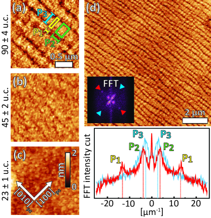
The pattern that we observe at the surface of the SrRuO3 top layer is comparable to what has been seen in PbTiO3 layers grown on DyScO3 substrates in Ref Nesterov-APL-2013 , attributed to the presence of periodic ferroelastic domains. To extract the period of the distortions visible on the surface of the samples, we calculate the fast Fourier transform (FFT) of the autocorrelation image, as shown in Figure 2(d) for the sample with the 90 u.c. thick PbTiO3 layer. Along DyScO3 (red), two periods are visible, P1 = 77 1 nm and P2 = 280 3 nm, while along DyScO3 (blue), a unique period P3 = 335 4 nm is visible. These periods have been illustrated on the topography image of the corresponding sample as yellow (with dimensions P1 P3) and green (with dimensions P2 P3) rectangles. All these values are reported in Table S1 (Supplementary Materials).
II.2 Domain structures observed by scanning transmission electron microscopy
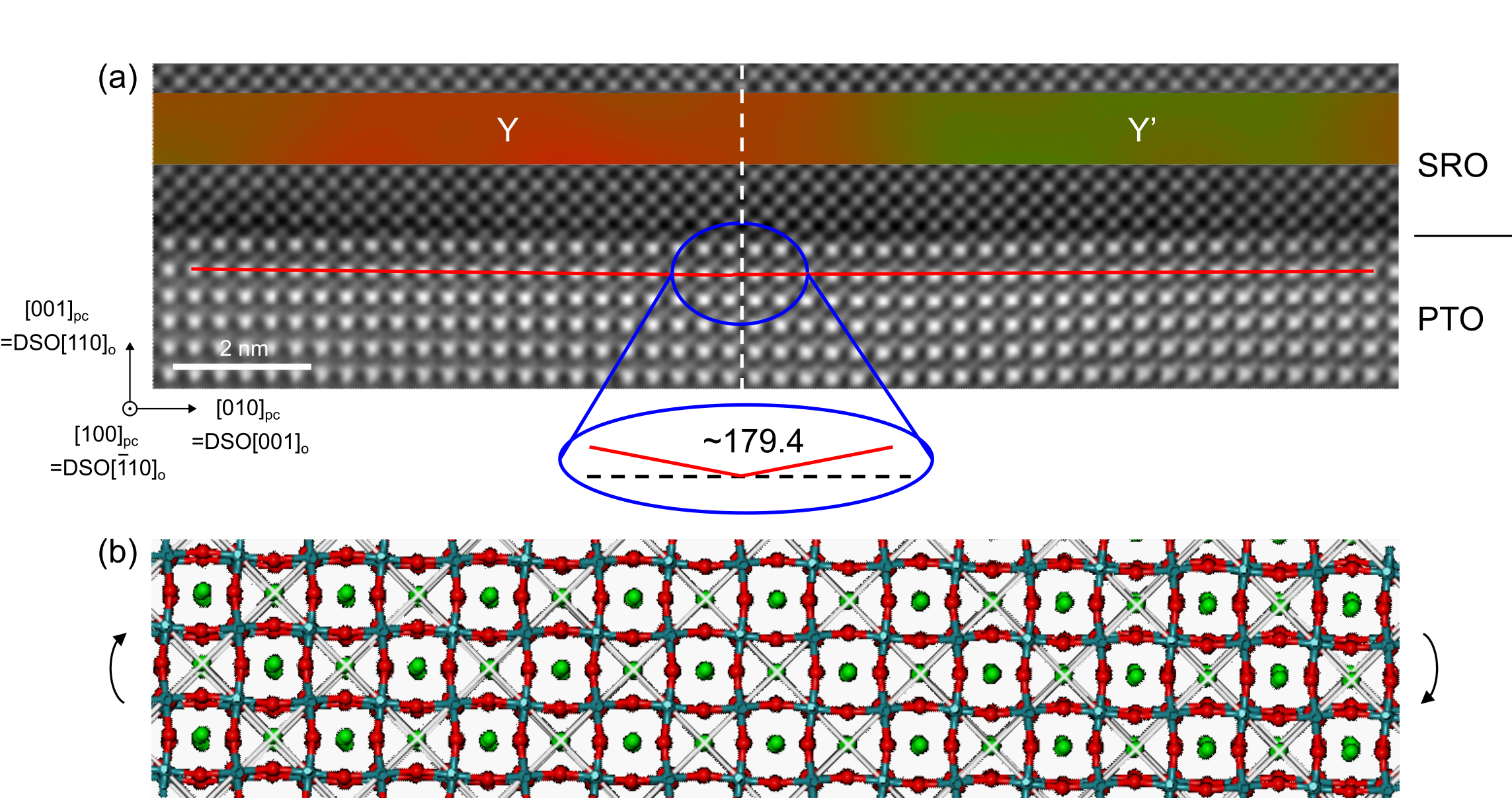
To better understand the origin of this pattern visible at the surface of the SrRuO3 top layer, we turned to cross-sectional scanning transmission electron microscopy (STEM) images. The three samples were cut and prepared for STEM measurements to obtain slices in the plane defined by the (horizontal direction) and (vertical direction) axes of DyScO3. STEM images were obtained using bright field (BF), annular bright field (ABF), medium angle annular dark field (MAADF) and high-angle annular dark field (HAADF) detectors along the DyScO3 zone-axis (see section IV.3 for more technical details).
The domain walls in the PbTiO3 layers can be directly seen in the STEM images, as shown in Figure 3 (a-c - HAADF images) and in Figure 6 (a-c - BF images), while the SrRuO3 layers appear rather homogeneous. The PbTiO3 layers in the three samples studied have different domain configurations, where the expected pattern for the thicker PbTiO3 layer transforms into a flux-closure pattern for the thinner PbTiO3 layers (see Ref. Lichtensteiger-APLMaterials-2023 for a complete x-ray diffraction based investigation of ferroelectric domain configuration in an extended series of samples).
II.2.1 Geometric Phase Analysis
To study the local strain induced by these different domain configurations, we turn to Geometric Phase Analysis (GPA) Hytch-Ultramicroscopy-1998 . This is done by taking the FFT of the HAADF-STEM images in Figure 3, selecting two peaks (here and ) corresponding to two reciprocal lattice vectors defining the lattice, and getting the inverse Fourier transform containing information about local displacements of the atomic planes along these two vectors. The local strain components are calculated from the derivative of the obtained displacement field: in-plane strain (along DyScO3), out-of-plane strain (along DyScO3), shear strain and rotation .
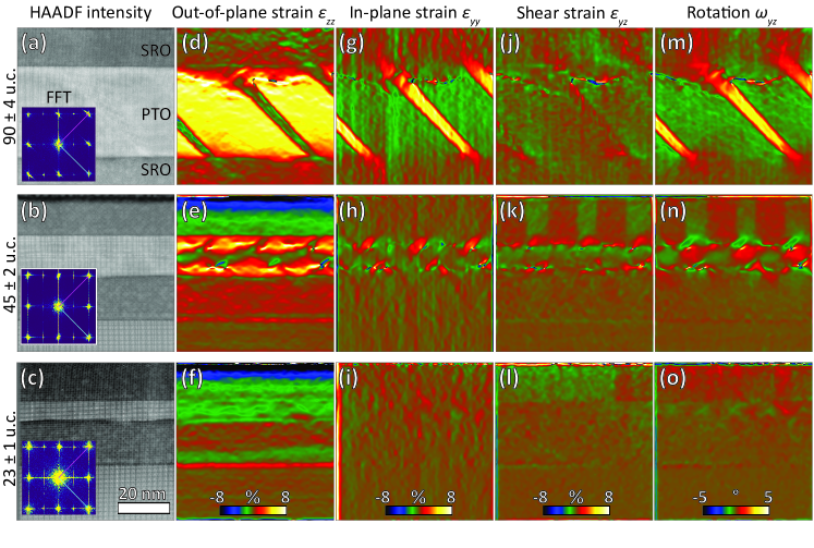
Looking first at the results within the PbTiO3 layers, we see from the HAADF images and from the GPA maps that the domain patterns vary with PbTiO3 thickness. For the 90 u.c. thick PbTiO3 in Figure 3 (top row), we see large regions with a high out-of-plane strain, but low in-plane strain, shear and rotation, corresponding to -domains, i.e. regions where the polarisation is out-of-plane. These regions are separated by narrower features, with high in-plane strain and rotation, but low out-of-plane strain and shear, corresponding to -domains, i.e. regions where the polarisation is in-plane. These results confirm a typical well developed -phase. For the 45 u.c. thick PbTiO3 layer in Figure 3 (center row), the strain map is more complex, with alternating regions with large out-of-plane strain or large in-plane strain close to each interface, and reduced strain at the center of the PbTiO3 layer, clearly different from an -phase (see Supplementary Materials Figure S4). This pattern is more comparable to the flux closure configuration observed for PbTiO3 with similar thickness grown without electrodes Tang-Science-2015 . Finally, for the 23 u.c. thick PbTiO3 layer in Figure 3 (bottom row), the PbTiO3 strain maps are more homogeneous compared to the results obtained for the two other samples. This indicates that for this sample, the distortions related to the ferroelectric/ferroelastic domain configuration in the PbTiO3 layer are small with respect to the homogeneous strain induced by the substrate. The most pronounced contrast is visible in the rotation map and corresponds to a pattern with a period of 16 nm, in agreement with the value found by XRD (see Supplementary Materials Figure S3 and Table S1 for comparison).
Concentrating now on the SrRuO3 layers, we see that the bottom ones are predominantly homogeneous in all three samples. However, this is not the case for the top SrRuO3 layers, where different contrasts appear for the three different PbTiO3 thicknesses. While the SrRuO3 layer on top of the 23 u.c. PbTiO3 looks rather homogeneous, regions with different shear strain and rotation values alternate in the SrRuO3 layers grown on top of the 45 u.c. and 90 u.c. PbTiO3 with boundaries propagating along the [001]pc growth direction.
For the sample with 90 u.c. PbTiO3, at the interface with each -domain and above the obtuse angle formed by the domain wall, the rotation is positive (red), while it is negative (green) above the acute angle (Figure 3(m)). The rotation then propagates directly to the top surface along the growth direction DyScO3. A similar modulation of the rotation is also observed in the SrRuO3 bottom electrode, with positive rotation below the obtuse angle of the domain wall, and negative rotation below the acute angle. However, for the bottom electrode, this modulation is limited to the vicinity of the interface and does not propagate through the whole SrRuO3 bottom electrode thickness, most likely due to substrate clamping.
For the sample with 45 u.c. PbTiO3, regions with a positive rotation (red) alternate with regions with a negative rotation (green) (Figure 3(n)), with a reduced rotation amplitude compared to the sample with 90 u.c. thick PbTiO3, but with sharper boundaries. The period of this pattern follows the period of the ferroelectric domains underneath.
II.2.2 Discriminating between and using fast Fourier transforms
To better understand the origin of this contrast, one can use the FFT and deduce the orientation of the SrRuO3 layers from the obtained Bragg peak positions. In the FFT images in Figure 4, the bright peaks of the pseudo-cubic lattice are clearly visible, corresponding to {0 k l}pc with and integer indices. Additionally to these peaks, weaker peaks also appear at positions corresponding to half-integer Miller indices {0 1/2 1/2}pc highlighted in blue and {0 1/2 1}pc highlighted in yellow. These peaks come from the orthorhombic unit cell, which is composed of 4 pseudo-cubic unit cells, as described in Figure 1. The position of the additional peaks is a clear indication of the orientation of the orthorhombic unit cell. The {0 1/2 1}pc peaks in the FFT appear when the orthorhombic long axis [001]o is oriented in-plane, parallel to the [010]pc axis, and correspond to the or orientation (note that it is not possible to discriminate between or in this measurement geometry). The {0 1/2 1/2}pc peaks on the other hand are the signature of the orthorhombic long axis [001]o being oriented in-plane, parallel to the [100]pc axis, corresponding to or orientation.
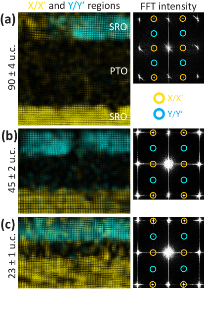
By selecting the different half order peaks and reconstructing the images in Figure 4, we find that the {0 1/2 1}pc peaks corresponding to orientation originate from the substrate and the bottom SrRuO3 electrode for all three samples, while the {0 1/2 1/2}pc peaks corresponding to originate from the top SrRuO3 electrode. We also note that for the sample with the thickest PbTiO3 layer, the top SrRuO3 shows a mixed and character. Although already highlighting differences in the top SrRuO3 layers for the different samples, this is not enough yet to explain the contrast observed in the strain and rotation maps in the GPA analysis in the SrRuO3 top layers for the samples with 45 u.c. and 90 u.c. thick PbTiO3 layers. This will be further investigated below, where we show that it is possible to discriminate between and 222Although the orientation of the lamella does not allow us to discriminate between and , we can go one step further by discriminating between and , the two orientations corresponding to very small horizontal shift in the peak positions..
II.2.3 Discriminating between and using fast Fourier transforms
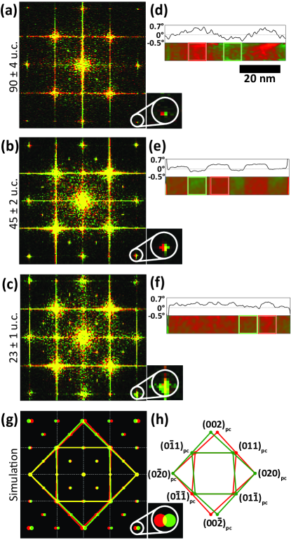
FFT was performed locally on selected regions corresponding to different shear strain and rotation values in the top SrRuO3 layers of the three samples, as shown in Figure 5. The regions of interest are selected based on the largest contrast in the GPA rotation maps in Figure 5(d-f), and give the colored diffraction patterns in (a-c) for the sample with 90 u.c. (a), 45 u.c. (b) and 23 u.c. (c) PbTiO3 , respectively, combining the FFT Bragg peaks in red and in green from the two regions. For the samples with 90 u.c. and 45 u.c. PbTiO3 , the two diffraction patterns do not overlap perfectly, and a very small horizontal shift can be observed (the peak is enlarged for clarity). For comparison, the diffraction pattern has been simulated for the and orientations by arbitrarily increasing the difference between the and parameters ( and in arbitrary units), making the difference in the Bragg peak positions more visible: the difference between and results in horizontal shifts of peaks, as measured experimentally. No shift is observed for the SrRuO3 top electrode above 23 u.c. PbTiO3. From this we can conclude that the contrast seen in the GPA strain and rotation maps for the two samples with the thickest PbTiO3 layers arises from alternating and domains. Moreover, Figure 5(d) shows that the transition from to domains for the sample with 90 u.c. PbTiO3 is gradual with a modulation of the rotation following a sinusoidal behavior between 0.3∘ and -0.3∘ with a period of approximately 30 nm. In comparison, this transition is much sharper for the sample with the 45 u.c. PbTiO3 layer, with the modulation of the rotation following a step-like function between 0.15∘ to -0.2∘ with a period of approximately 20 nm as seen in Figure 5(e), hinting at the presence of proper twin boundaries between and domains. Further discussion and high resolution TEM image of such a twin boundary is shown in Supplementary Materials, Section S4.
III Discussion
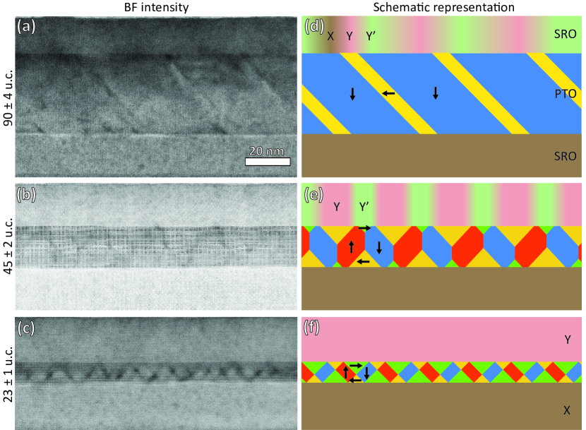
We show that the complex tilt pattern of the PbTiO3 layer is responsible for the deformation of the SrRuO3 layer deposited on top, resulting in the periodic pattern visible in the topography by AFM. Our STEM measurements highlight how the domain pattern in the PbTiO3 layer affects the strain state and crystal orientation in the SrRuO3 top layer, with clear differences for the three samples with different PbTiO3 layer thickness.
We find that the top SrRuO3 layers show a different behaviour for each of the three samples, summarized in Figure 6, while the bottom SrRuO3 layers systematically have the same orientation as the DyScO3 substrate (-orthorhombic orientation), probably pinned by the interfacial continuity of the oxygen octahedral rotation imposed by the substrate.
For the sample with a 23 u.c. PbTiO3 layer, where no pattern is visible in the topography, we observe a flux-closure type PbTiO3 domain structure and correspondingly a null or weakly distorted SrRuO3 structure, homogeneously in the -orthorhombic orientation as shown in Figure 6 (bottom row).
For the sample with a 45 u.c. PbTiO3 layer, where a pattern is only weakly observed in the topography, we again have a flux-closure type PbTiO3 domain structure. However, in Figure 3 if we compare the out-of-plane (e) and in-plane (h) strain maps close to the interfaces, the strain pattern locally resembles that of the phase (Figure 3 (g-h)). This points at a nascent phase near the top interface, allowing a more pronounced deformation that translates into a clearly distorted SrRuO3 structure that shares the same periodicity as the PbTiO3. The top SrRuO3 thus alternates between - and -orthorhombic orientations - with a period corresponding to the period of the domain pattern in PbTiO3. The mechanism that drives the rotation of the top SrRuO3 is strain-induced: due to the small shear and rotation in the top layer of PbTiO3, the PbTiO3/top SrRuO3 interface is not totally flat (left and right inclination). The formation of domains is a good way to minimize the interface strain (Figure 6(center row)).
Finally, in the sample with the 90 u.c. thick PbTiO3 layer, where the topography displays noticeable tilts and trenches, the -phase is fully developed, with strong PbTiO3 lattice heterogeneity that partially imprints on the top SrRuO3 electrode. Here the top SrRuO3 exhibits domains with alternating primary - and - orthorhombic orientations, and some interstitial regions. The positive and negative rotation on the SrRuO3 correspond to and domains as evidenced by the GPA shear strain and rotation maps. In between these and domains, a very tiny region with a typical -orientation is often observed in the FFT. This is typically restrained to a 10 nm width domain at the interface between and domains where no rotation was observed on the GPA map. It is different from the case with the 45 u.c. thick PbTiO3 layer, where sharp interfaces and no oriented domain were observed between and domains.
Our work demonstrates that the large structural distortions associated with ferroelastic domains propagate through the top SrRuO3 layer, creating a modulated structure that extends beyond the ferroelectric layer thickness, allowing domain engineering in the top SrRuO3 electrode. Since there exists a one-to-one correspondence between the structural and magnetic domains Wang-NPJQuantMats-2020 , our approach allows magnetic domain engineering in SrRuO3 thin films through structural domain engineering to be realized. This work paves a new path towards control of magnetic domains via structural coupling to ferroelastic domains.
IV Experimental techniques
IV.1 Sample growth
The three samples were deposited using our in-house constructed off-axis radio-frequency magnetron sputtering system, equipped with three different guns allowing the deposition of heterostructures and solid-solutions of high crystalline quality. PbTiO3 thin films were deposited at 560∘C, in 180 mTorr of a 20:29 O2/Ar mixture, at a power of 60 W, and using a Pb1.1TiO3 target with 10% excess of Pb to compensate for its volatility. SrRuO3 layers were deposited from a stoichiometric target in 100 mTorr of O2/Ar mixture of ratio 3:60, at a power of 80 W. The bottom layer was grown at 640∘C, while for the top layer the temperature was kept at the growth temperature used for PbTiO3, i.e. 560∘C, to avoid possible damage of the PbTiO3 layer. Huettinger PFG 300 RF power supplies are used in power control mode. The sample holder is grounded during deposition, but the sample surface is left floating.
IV.2 Atomic force microscopy
Topography measurements were performed using a Digital Instrument Nanoscope Multimode DI4 with a Nanonis controller.
IV.3 Scanning transmission electron microscopy
Cross-sectional slices prepared by focus ion beam allow the imaging of domain structures by scanning transmission electron microscopy. Experiments were acquired on Nion Cs-corrected UltraSTEM200 at 100 kV operating voltage. A convergence angle of 30 mrad was used to allow high-resolution atomic imaging with a typical spatial resolution of 1 Å. Three imaging detectors in the STEM are used to simultaneously obtain bright field, annular bright field or medium angle annular dark field, and high angle annular dark field images. For ABF-MAADF imaging, the inner-outer angles can be continuously adjusted between 10-20 to 60-120 mrad. Most ABF images were collected with 15-30 mrad and MAADF images with 40-80 mrad angular ranges.
For the high-resolution HAADF images used to extract GPA, to minimize the influence of the sample drift and environmental noise, a series of fast-scan (low exposure time) HAADF images was taken in the same region; afterward, a script based on Gatan DigitalMicrograph software aligned and summed them together. This technique typically used twenty 4kx4k images with 1s exposure time per pixel.
GPA is an algorithm that reconstructs the displacement field from HAADF images by measuring the displacement of lattice fringes with respect to a reference lattice here chosen as the substrate. GPA thus allows the local strain present in the different layers to be revealed: in-plane strain (along [010]pc, i.e. perpendicular to the growth direction), out-of-plane strain (along [001]pc i.e. along the growth direction), shear strain and rotation . This is particularly useful for the study of the domain configuration in PbTiO3, as the polarisation is related to the strain from the strong strain-polarisation coupling Cohen-Ferroelectrics-1992 . At room temperature, PbTiO3 is tetragonal with the polarisation pointing along the long tetragonal axis. The strain orientation and amplitude therefore indicates the orientation and magnitude of the polarisation.
We determine the periodicity of the superstructures in the PbTiO3 and SrRuO3 layers by measuring the distances between the additional reciprocal space spots obtained after FFT. The accuracy of the measurement was estimated by considering the diffraction spot extension as the lower and upper limit for the superstructure length estimation.
IV.4 X-ray diffraction
In-house XRD measurements were performed using a Panalytical X’Pert diffractometer with Cu K radiation (1.5405980 Å) equipped with a 2-bounce Ge(220) monochromator and a triple axis detector in our laboratory in Geneva. The -2 scans were analysed using the InteractiveXRDFit software Lichtensteiger-JApllCryst-2018 . This XRD system is also equipped with a PIXcel 1D detector, used for faster acquisition of the reciprocal space maps.
V Data availability
The data that support the findings of this study are available at Yareta (DOI).
VI Acknowlegements
The authors thank Lukas Korosec and Christian Weymann for support and discussions.
This work was supported by Division II of the Swiss National Science Foundation under projects 200021_178782 and 200021_200636. STEM experiments were supported by the EU Horizon research and innovation program under grant agreement ID 823717-ESTEEM3. C.-P. Su acknowledges Taiwan Paris-Saclay doctoral scholarship, which is cost-shared by the Ministry of Education, Taiwan, and the Université Paris-Saclay, France. M.H. acknowledges funding from the SNSF Scientific Exchanges Scheme (Grant Number IZSEZ0_212990).
VII Author contributions
C.L, M.H., A.G. and J.M.T. designed the experiment. C.L., M.H. and L.T. grew the samples and conducted the AFM and XRD measurements and analysis. C.-P.S. and A.G. conducted the STEM measurements. I.G., C.-P.S. and A.G. performed advanced STEM analysis. C.L. wrote the manuscript with contributions from all authors. All authors discussed the experimental results and models, commented on the manuscript, and agreed on its final version.
VIII Bibliography
References
- (1) Ahn, C. H. et al. Ferroelectric field effect in epitaxial thin film oxide SrCuO 2/Pb(Zr0.52Ti0.48)O3 heterostructures. Science 269, 373–376 (1995).
- (2) Eom, C. et al. Single-Crystal Epitaxial Thin Films of the Isotropic Metallic Oxides Sr 1-x Ca x RuO 3 (0 x 1). Science 258, 1766–1769 (1992).
- (3) Cao, G., McCall, S., Shepard, M., Crow, J. & Guertin, R. Thermal, magnetic, and transport properties of single-crystal Sr1-xCaxRuO3 (0<=x<=1.0). Physical Review B - Condensed Matter and Materials Physics 56, 321–329 (1997).
- (4) Wang, L. et al. Ferroelectrically tunable magnetic skyrmions in ultrathin oxide heterostructures. Nature Materials 17, 1087–1094 (2018). URL http://dx.doi.org/10.1038/s41563-018-0204-4.
- (5) Seddon, S. D. et al. Real-space observation of ferroelectrically induced magnetic spin crystal in SrRuO3. Nature Communications 12, 1–7 (2021). URL http://dx.doi.org/10.1038/s41467-021-22165-5.
- (6) Koster, G. et al. Structure, physical properties, and applications of SrRuO 3 thin films. Reviews of Modern Physics 84, 253–298 (2012).
- (7) Jiang, J. C., Tian, W., Pan, X., Gan, Q. & Eom, C. B. Effects of miscut of the SrTiO3 substrate on microstructures of the epitaxial SrRuO3 thin films. Materials Science and Engineering B 56, 152–157 (1998).
- (8) Jiang, J. C., Tian, W., Pan, X. Q., Gan, Q. & Eom, C. B. Domain structure of epitaxial SrRuO3 thin films on miscut (001) SrTiO3 substrates. Applied Physics Letters 72, 2963–2965 (1998).
- (9) Vailionis, A., Siemons, W. & Koster, G. Room temperature epitaxial stabilization of a tetragonal phase in ARu O3 (A=Ca and Sr) thin films. Applied Physics Letters 93, 1–4 (2008).
- (10) Zakharov, N. D., Satyalakshmi, K. M., Koren, G. & Hesse, D. Substrate temperature dependence of structure and resistivity of SrRuO3 thin films grown by pulsed laser deposition on (100) SrTiO3. Journal of Materials Research 14, 4385–4394 (1999).
- (11) Wang, W. et al. Magnetic domain engineering in SrRuO3 thin films. npj Quantum Materials 5, 1–7 (2020).
- (12) Tang, Y. et al. Periodic Polarization Waves in a Strained, Highly Polar Ultrathin SrTiO3. Nano Letters 21, 6274–6281 (2021).
- (13) Hadjimichael, M. et al. Metal–ferroelectric supercrystals with periodically curved metallic layers. Nature Materials 20, 495—-502 (2021).
- (14) Pertsev, N. A., Zembilgotov, A. G. & Tagantsev, A. K. Effect of Mechanical Boundary Conditions on Phase Diagrams of Epitaxial Ferroelectric Thin Films. Physical Review Letters 80, 1988–1991 (1998).
- (15) Pertsev, N. A. & Koukhar, V. G. Polarization instability in polydomain ferroelectric epitaxial thin films and the formation of heterophase structures. Physical Review Letters (2000).
- (16) Koukhar, V. G., Pertsev, N. A. & Waser, R. Thermodynamic theory of epitaxial ferroelectric thin films with dense domain structures. Physical Review B - Condensed Matter and Materials Physics 64, 1–15 (2001). eprint 0102460.
- (17) Li, Y. L., Hu, S. Y., Liu, Z. K. & Chen, L. Q. Phase-field model of domain structures in ferroelectric thin films. Applied Physics Letters 78, 3878–3880 (2001).
- (18) Jiang, Z. et al. Strain-induced control of domain wall morphology in ultrathin PbTiO3 films. Physical Review B - Condensed Matter and Materials Physics 89, 35–37 (2014).
- (19) Chapman, J. B., Kimmel, A. V. & Duffy, D. M. Novel high-temperature ferroelectric domain morphology in PbTiO3 ultrathin films. Physical Chemistry Chemical Physics 19, 4243–4250 (2017).
- (20) Schlom, D. G. et al. Strain Tuning of Ferroelectric Thin Films. Annual Review of Materials Research 37, 589–626 (2007).
- (21) Kittel, C. Theory of the structure of ferromagnetic domains in films and small particles. Physical Review 70, 965–971 (1946).
- (22) Lichtensteiger, C., Fernandez-Pena, S., Weymann, C., Zubko, P. & Triscone, J. M. Tuning of the depolarization field and nanodomain structure in ferroelectric thin films. Nano Letters 14, 4205–4211 (2014). eprint 1507.08498.
- (23) Lichtensteiger, C., Weymann, C., Fernandez-Pena, S., Paruch, P. & Triscone, J. M. Built-in voltage in thin ferroelectric PbTiO3 films: The effect of electrostatic boundary conditions. New Journal of Physics 18 (2016).
- (24) Yadav, A. K. et al. Observation of polar vortices in oxide superlattices. Nature 530, 198–201 (2016). URL http://dx.doi.org/10.1038/nature16463.
- (25) Stoica, V. A. et al. Optical creation of a supercrystal with three-dimensional nanoscale periodicity. Nature Materials 18, 377–383 (2019).
- (26) Hadjimichael, M. Ferroelectric domains in lead titanate heterostructures. Ph.D. thesis, University College London (2019).
- (27) Gonçalves, M. A., Escorihuela-Sayalero, C., Garca-Fernández, P., Junquera, J. & Íñiguez, J. Theoretical guidelines to create and tune electric skyrmion bubbles. Science Advances 5, 1–6 (2019).
- (28) Das, S. et al. Observation of room-temperature polar skyrmions. Nature 568, 368–372 (2019).
- (29) Wang, Y. J. et al. Polar meron lattice in strained oxide ferroelectrics. Nature Materials (2020).
- (30) Íñiguez, J., Zubko, P., Luk’yanchuk, I. & Cano, A. Ferroelectric negative capacitance. Nature Reviews Materials 4 (2019).
- (31) Vlooswijk, A. H. et al. Smallest 90° domains in epitaxial ferroelectric films. Applied Physics Letters 91, 20–23 (2007). eprint 0706.2487.
- (32) Catalan, G. et al. Flexoelectric rotation of polarization in ferroelectric thin films. Nature Materials 10, 963–967 (2011). URL http://dx.doi.org/10.1038/nmat3141.
- (33) Nesterov, O. et al. Thickness scaling of ferroelastic domains in PbTiO3 films on DyScO3. Applied Physics Letters 103, 142901 (2013).
- (34) Lichtensteiger, C. et al. Mapping the complex evolution of ferroelastic/ferroelectric domain patterns in epitaxially strained PbTiO3 heterostructures. APL Materials 11, 000000 (2023).
- (35) Veličkov, B., Kahlenberg, V., Bertram, R. & Bernhagen, M. Crystal chemistry of GdScO3, DyScO3, SmScO 3 and NdScO3. Zeitschrift fur Kristallographie 222, 466–473 (2007).
- (36) Randall, J. J. & Ward, R. The Preparation of Some Ternary Oxides of the Platinum Metals. Journal of the American Chemical Society 81, 2629–2631 (1959).
- (37) Glazer, A. M. The classification of tilted octahedra in perovskites. Acta Crystallographica Section B Structural Crystallography and Crystal Chemistry 28, 3384–3392 (1972).
- (38) Woodward, P. M. Octahedral Tilting in Perovskites. I. Geometrical Considerations. Acta Crystallographica Section B: Structural Science 53, 32–43 (1997).
- (39) Although the strain with respect to is compressive, the system is usually referred to as being under tensile strain because the lattice parameter of DyScO3 is larger than the bulk = axes of PbTiO3.
- (40) Highland, M. J. et al. Interfacial charge and strain effects on the ferroelectric behavior of epitaxial (001) PbTiO3 films on (110) DyScO3 substrates. Applied Physics Letters 104, 1–4 (2014).
- (41) Junquera, J. & Ghosez, P. Critical thickness for ferroelectricity in perovskite ultrathin films. Nature 422, 506–509 (2003).
- (42) Aguado-Puente, P. & Junquera, J. Ferromagneticlike closure domains in ferroelectric ultrathin films: First-principles simulations. Physical Review Letters 100, 1–4 (2008).
- (43) Stengel, M., Vanderbilt, D. & Spaldin, N. A. Enhancement of ferroelectricity at metal-oxide interfaces. Nat. Mater. 8, 392–397 (2009).
- (44) Li, S. et al. Periodic arrays of flux-closure domains in ferroelectric thin films with oxide electrodes. Applied Physics Letters 111 (2017).
- (45) Hadjimichael, M., Li, Y., Yedra, L., Dkhil, B. & Zubko, P. Domain structure and dielectric properties of metal-ferroelectric superlattices with asymmetric interfaces. Physical Review Materials 4, 1–8 (2020).
- (46) Tang, Y. L. et al. Observation of a periodic array of flux-closure quadrants in strained ferroelectric PbTiO3 films. Science 348, 547–551 (2015).
- (47) Li, S. et al. Evolution of flux-closure domain arrays in oxide multilayers with misfit strain. Acta Materialia 171, 176–183 (2019).
- (48) Hÿtch, M. J., Snoeck, E. & Kilaas, R. Quantitative measurement of displacement and strain fields from HREM micrographs. Ultramicroscopy 74, 131–146 (1998).
- (49) Although the orientation of the lamella does not allow us to discriminate between and , we can go one step further by discriminating between and , the two orientations corresponding to very small horizontal shift in the peak positions.
- (50) Cohen, R. E. & Krakauer, H. Electronic structure studies of the differences in ferroelectric behavior of batiO3 and pbtiO3. Ferroelectrics (1992).
- (51) Lichtensteiger, C. InteractiveXRDfit: A new tool to simulate and fit X-ray diffractograms of oxide thin films and heterostructures. Journal of Applied Crystallography 51, 1745–1751 (2018).
Supplementary Materials
S1 Orthorhombic orientation
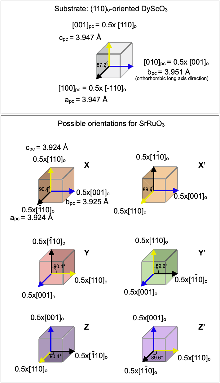
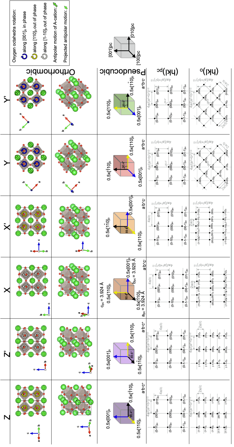
In Figure S2, the six possible orthorhombic orientations of the SrRuO3 on (110)o-oriented DyScO3 substrate (in space group) are represented. Each column corresponds to a different orientation , , , , and . First row: projection along [100]pc. The oxygen octahedra rotations are represented as blue (in-phase along the [001]o axis), yellow (out of phase along the [110]o axis) and white (out of phase along the axis) rotating arrows, and the antipolar motion of the A-cations are represented by green straight arrows. Second row: perspective view. , and correspond to the axis of the orthorhombic unit cell. Third row: corresponding pseudocubic representation. Forth row: reciprocal space representation and (hkl)pc indices corresponding to the pseudocubic structure. Fifth row: reciprocal space representation and (hkl)o indices corresponding to the orthorhombic structure structure, highlighting the position of the “half-order” peaks.
S2 X-ray diffraction data for the three samples
S3 Table summarizing the different periods
| PbTiO3 | Period in PbTiO3 | Period in PbTiO3 | Period in SrRuO3 | Period |
|---|---|---|---|---|
| thickness | from XRD | from STEM | from STEM | from topo |
| (u.c.) | (nm) | (nm) | (nm) | (nm) |
| 23 1 | 14.3 0.1 | 13 1 | n.a. | n.a. |
| 45 2 | 23.4 0.2 | 26 1 | 25 1 | n.a. |
| 90 4 | 44 3 (146.4 0.3) | 46 3 | 80 30 | 77 1 (280 3) |
S4 Twin boundary observed by GPA and HAADF in the SrRuO3 top electrode above the 45 u.c. thick PbTiO3 layer
As mentioned in the paper, the strain map for the 45 u.c. thick PbTiO3 layer in Figure 3 (center row) is complex, with regions alternating with large out-of-plane strain or large in-plane strain close to each interface, and reduced strain at the center of the PbTiO3 layer. The succession of sequences close to the interfaces resembles with local -domains, but with an offset of about half a period between the sequences at the top and at the bottom interface. In the center of the layer the out-of-plane extension is rather weak, while periodic strain contrasts are present and alternating rotations are visible in the GPA maps. It is clearly different from the expanded -phase of the 90 u.c. thick PbTiO3. Horizontal flux-closure quadrants as observed for PbTiO3 with similar thickness grown without electrodes Tang-Science-2015 will give resembling features, but does not explain the local -domains at the interface, hinting at a more complicated three-dimensional flux-closure domain. For instance, combination of “horizontal” and “vertical” flux closures have already been reported in metal-ferroelectric superlattices to minimize the macroscopic polarisation for imperfect electrode while still competing with -pattern at longer scale Hadjimichael-NatMat-2021 . Such combination can explain the strong flux closure contrast from the HAADF and MAADF STEM images and the presence of nascent local -phases at the interface. The complex shear strains and rotations in the PbTiO3 layer results in a distorted top interface, exhibiting staggered left or right inclination confirmed by the atomic-resolved HAADF image shown in Figure S4. The interface has a zigzag behaviour due to the presence of the small -domains, inducing SrRuO3 twinning. This image demonstrates how the growing domains near the top of the PbTiO3 film imposes the crystallographic domain distribution in the top SrRuO3 layer. The corresponding rotational and shear patterns of the top PbTiO3 part are thus corresponding to the and domains of the SrRuO3, as shown in Figure S4, both having the same periodicity (ca. 26 nm), sharing interface connectivity.