suppl \externaldocumentsuppl
Twist angle dependent electronic properties of exfoliated single layer MoS2 on Au(111)
Abstract
Synthetic materials and heterostructures obtained by the controlled stacking of exfoliated monolayers are emerging as attractive functional materials owing to their highly tunable properties. We present a detailed scanning tunneling microscopy and spectroscopy study of single layer MoS2-on-gold heterostructures as a function of twist angle. We find that their electronic properties are determined by the hybridization of the constituent layers and are modulated at the moiré period. The hybridization depends on the layer alignment and the modulation amplitude vanishes with increasing twist angle. We explain our observations in terms of a hybridization between the nearest sulfur and gold atoms, which becomes spatially more homogeneous and weaker as the moiré periodicity decreases with increasing twist angle, unveiling the possibility of tunable hybridization of electronic states via twist angle engineering.
The rapid increase in the number of 2D materials which can be exfoliated and the fantastic progress in their layer-by-layer stacking with controlled sequence [1] and twist angle [2, 3] open up exceptional opportunities to design new functional quantum materials. A famous example is twisted bilayer graphene, whose very rich phase diagram ranges from correlated insulating to superconducting phases depending on twist angle and electrostatic doping [4, 5]. Heterostructures with unique properties can also be obtained by stacking 2D exfoliated transition metal dichalcogenides (TMD) [6, 7, 8, 9].
Exfoliated 2D materials in direct proximity to a metal surface with selected twist angles offer further attractive materials engineering perspectives [10]. Such structures are challenging to prepare with a clean surface suitable for scanning tunneling microscopy (STM). Therefore, many STM studies to date have been carried out on epitaxial thin films grown in-situ by molecular beam epitaxy (MBE) or by chemical vapor deposition (CVD). The twist angle with the substrate of such films is set by thermodynamics and cannot be tuned at will. It is nearly 0∘ for 2H-MoS2 evaporated on Au(111) [11, 12, 13], one of the most studied TMD on a metallic substrate [14, 15].
Manual stacking of exfoliated monolayers allows to select arbitrary twist angles between the 2D material and the metallic substrate. Only a few STM studies of exfoliated 2H-MoS2 monolayers (hereafter simply MoS2) on Au(111) have been published [16, 17, 18, 19, 20, 21, 22], without any strong focus on twist angle dependent properties. Here, we present a detailed STM and scanning tunneling spectroscopy (STS) investigation of the electronic properties of MoS2 on Au(111) as a function of twist angle. We find that the semiconducting gap and band edges are modulated at the moiré period, with a modulation amplitude that vanishes with increasing twist angle. We explain our observations in terms of a hybridization between the sulfur and gold atoms, which becomes spatially more homogeneous and weaker as the moiré periodicity decreases with increasing twist angle.
I RESULTS
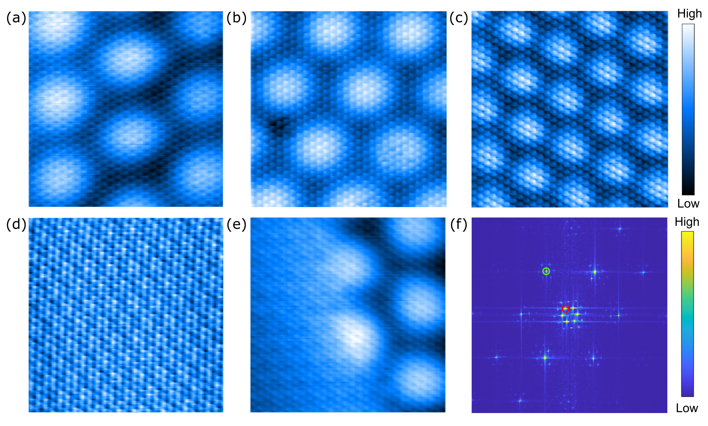
We performed STM and STS on continuous, millimeter-sized monolayer (ML) flakes obtained by exfoliating 2H-MoS2 [23] onto template-stripped Au substrates [24]. These substrates are poly-crystalline Au(111) films stripped from an ultra-flat silicon wafer (see Methods). STM and X-ray diffraction measurements show that they consist of Au(111) orientated grains, where different grains can be slightly tilted and rotated about their [111]-axis (see SI section \Romannum1). ML MoS2 on Au(111) is identified by its characteristic Raman spectrum [12, 25, 26] and from optical images where MoS2 appears darker on a bright Au substrate [27] (see SI section \Romannum1). A further confirmation that we have ML MoS2 is the observation of a moiré pattern in STM topography, which is absent for bilayer and thicker MoS2 flakes [11].
Exfoliating large area MoS2 MLs onto poly-crystalline Au(111) naturally produces regions with different twist angles between the two lattices. This provides a unique platform to characterize the electronic structure for different twist angles in a single sample, thus excluding potential sample-dependent fluctuations. Figure 1 shows typical raw data topographic STM images acquired in different regions of such a sample. They reveal the MoS2 lattice and the moiré patterns specific to the local twist angle (Figure 1(a)-(d) and SI Section \Romannum2). The corresponding Bragg and moiré peaks are highlighted in the Fourier transform (FT) of the 7.7° heterostructure by a green and a red circle, respectively (Figure 1(f)). The complete data set of Figure 1 is consistent with a large single crystal MoS2 ML, with a lattice oriented along a single direction, including across step edges and across gold grain boundaries (Figure 1(e) and SI Section \Romannum3).
We now turn to the spectroscopic characterization of MoS2 on Au(111) as a function of twist angle. Typical spectra measured on our devices are shown in Figure 2(a). They can be described as a modified semiconducting spectrum with a finite conductance in the gap region [17, 28]. We do not observe the spread in tunneling characteristics reported in previous STM experiments [17], most likely due to a cleaner MoS2/Au(111) interface exemplified by the perfect adherence of MoS2 to the substrate across grain boundaries and step edges (SI Section \Romannum3). We do find occasional bubbles [16, 18], where MoS2 is locally decoupled from the substrate (SI Section \Romannum4). These regions are electronically different, with a fully gaped semiconducting spectrum (Figure 2(a)) consistent with previous STM studies where MoS2 was not in direct contact with a metal surface [18, 29, 30, 31].
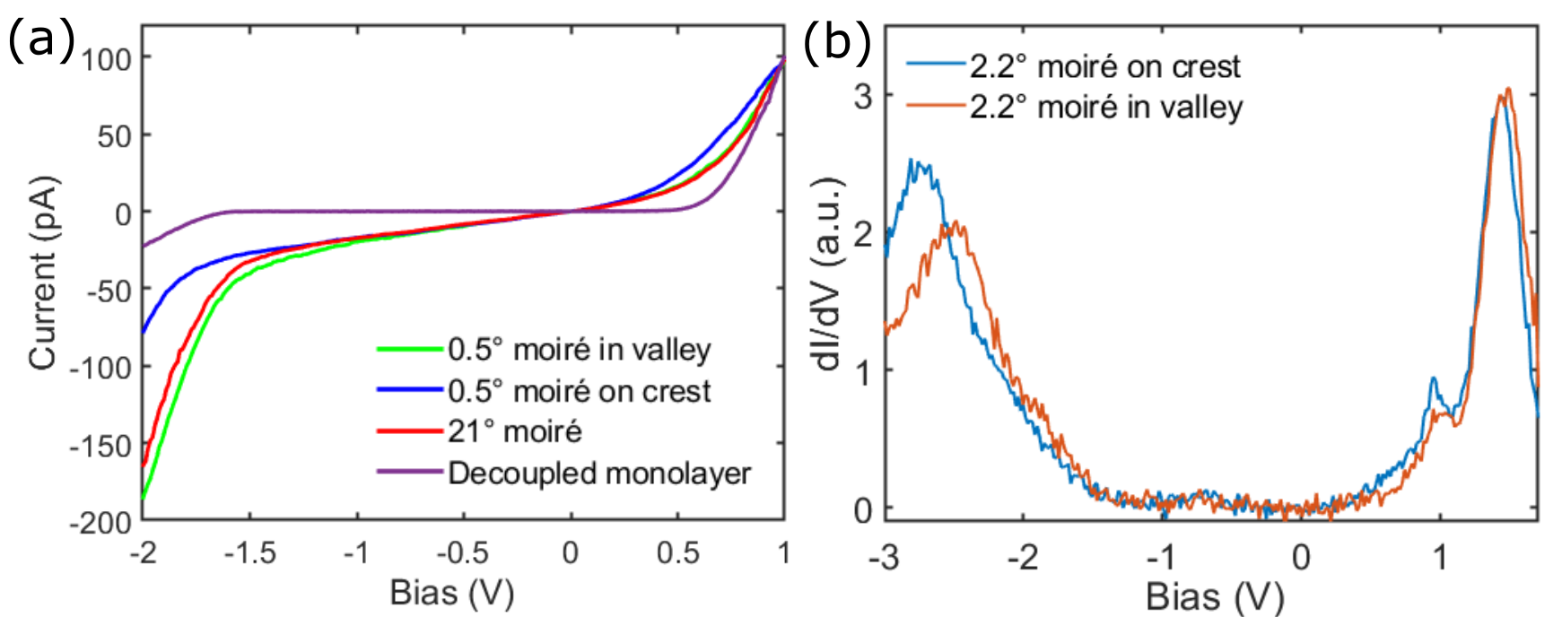
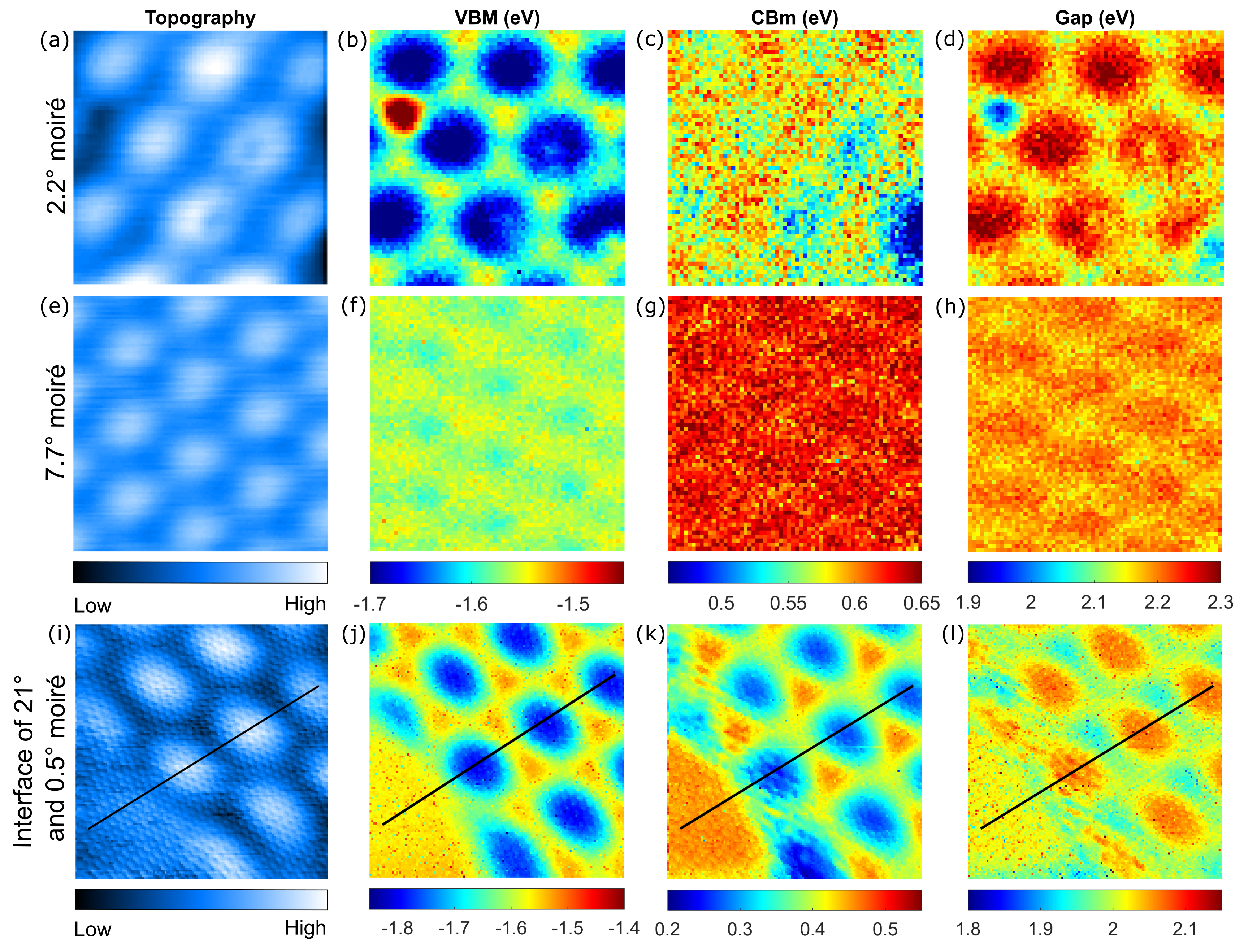
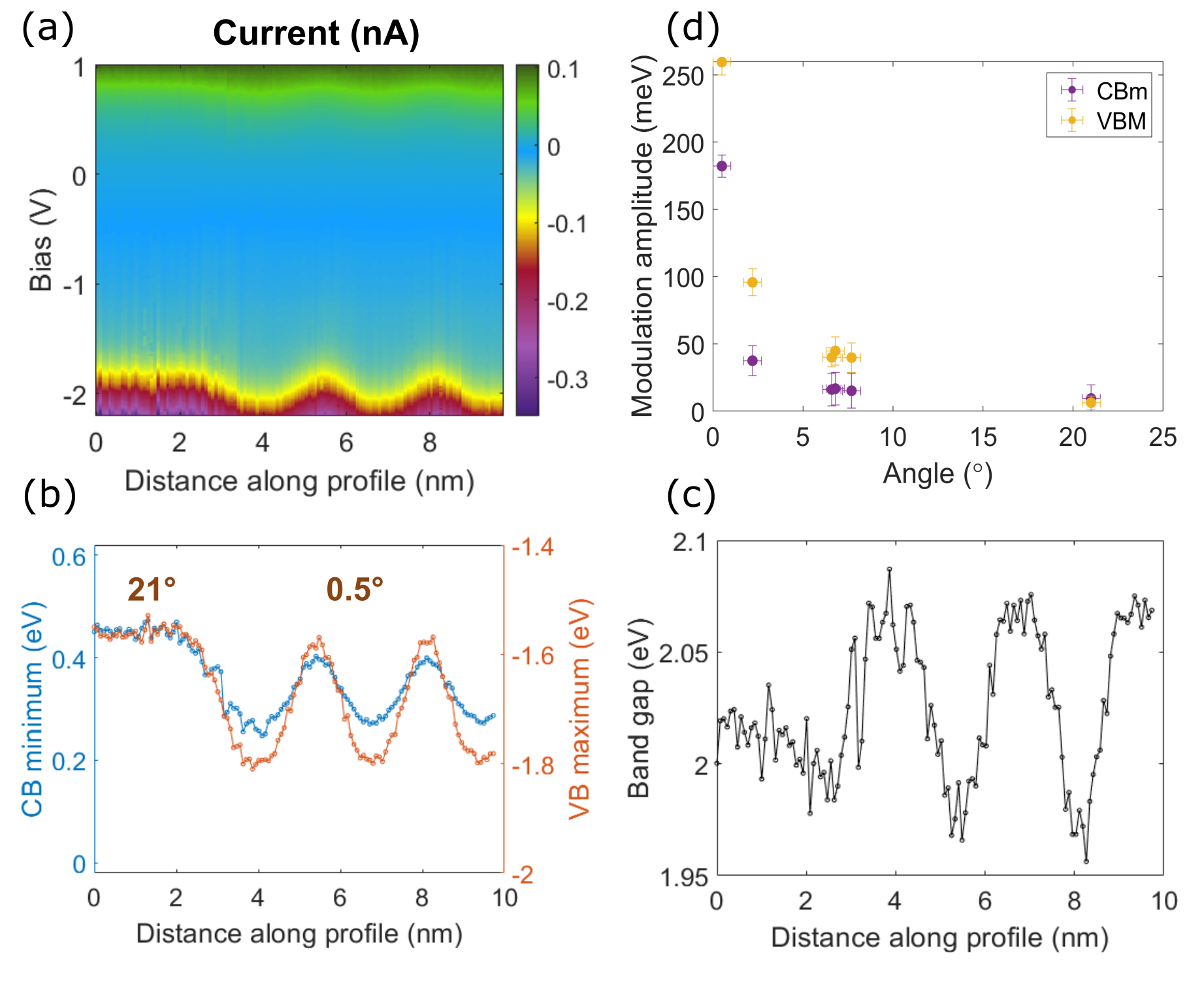
While the generic line shape is the same for all tunneling spectra measured on our MoS2/Au(111) heterostructures, we find some variations, in particular as a function of twist angle and as a function of position in the moiré unit. They are most prominent at negative bias below the Fermi level (), which corresponds to V in Figure 2. To characterize the twist angle dependence of the electronic properties of the MoS2/Au(111) heterostructures, we acquire and maps. For every tunneling conductance spectrum –two typical examples are shown in Figure 2(b)–, we fit the main peaks below (above) to a Gaussian and define the valence band maximum (conduction band minimum ) as the peak position plus (minus) its corresponding 2.2. Since the conductivity measured at these energies is predominantly related to states derived from MoS2 [32], we define as the gap. We find that amounts to about 2 eV in agreement with previous findings for MoS2 MLs grown on Au(111) [33, 34]. These three quantities are plotted alongside the corresponding topography for two different twist angles in Figure 3(a)-(h). Note that the same information can be obtained from the curves using a different fitting procedure (SI section \Romannum5) used in Figure 3(i)-(l) and in Figure 4(b)-(d).
The three main results of our experiments can be graphically seen in Figure 3: i) the local density of states (DOS) is modulated at the moiré pattern wavelength; ii) the modulation amplitude is significantly larger for the valence band than for the conduction band, and so is also modulated at the moiré pattern wavelength; iii) the modulation amplitude of and of are decreasing with increasing twist angle. The vanishing spatial modulations of the band edges and of the gap with increasing twist angle are most strikingly seen in Figure 3(i)-(l) and in Figure 4. They show a domain wall between a 21° and a 0.5° twist angle region spanned by a single MoS2 ML, which completely excludes any other origin than the twist angle for the observed differences. In Figure 4(b), we plot the modulation amplitudes of and –defined as the difference between maximum and minimum band edge energies for each twist angle– as a function of twist angle. The plot clearly shows the monotonic reduction of the and modulation amplitudes with increasing twist angle.
II Discussion
Density functional theory (DFT) calculations show that hybridization of MoS2 with Au(111) happens primarily through sulfur -orbitals and gold -orbitals, and that it is strongest when the two atoms are positioned atop each other (on-top alignment) [35]. Calculations further show that the hybridization mainly involves out-of-plane orbitals –which define the valence band (VB)– and less in-plane orbitals –which define the conduction band (CB)– [32]. This is consistent with the greater modulation of the VBM compared to the CBm in Figure 3 and in Figure 4(a)-(c). The modulation of the gap at the moiré periodicity in Figure 3(d),(h),(l) and in Figure 4(d) is a direct consequence of the different responses of the CB and of the VB to the hybridization. The effect is strongest in the middles of the bright moiré maxima seen in the topographic images in Figures 1 and 3. These moiré maxima must therefore correspond to the on-top alignment positions in the heterostructures, in agreement with previous assessments [33, 34].
Constant current STM images are a convolution of morphologic and electronic features [36]. Therefore, it is not a priori clear whether the moiré superstructure observed by STM is a structural or an electronic modulation. To address this question, we examined conductance maps as a function of bias. The fact that the moiré contrast does fully invert for certain bias ranges (SI Section \Romannum6) is not compatible with a structural modulation and provides strong evidence that the moiré pattern is of electronic origin in a flat MoS2 ML, in agreement with STM and X-ray standing wave measurement by Silva et al. [34].
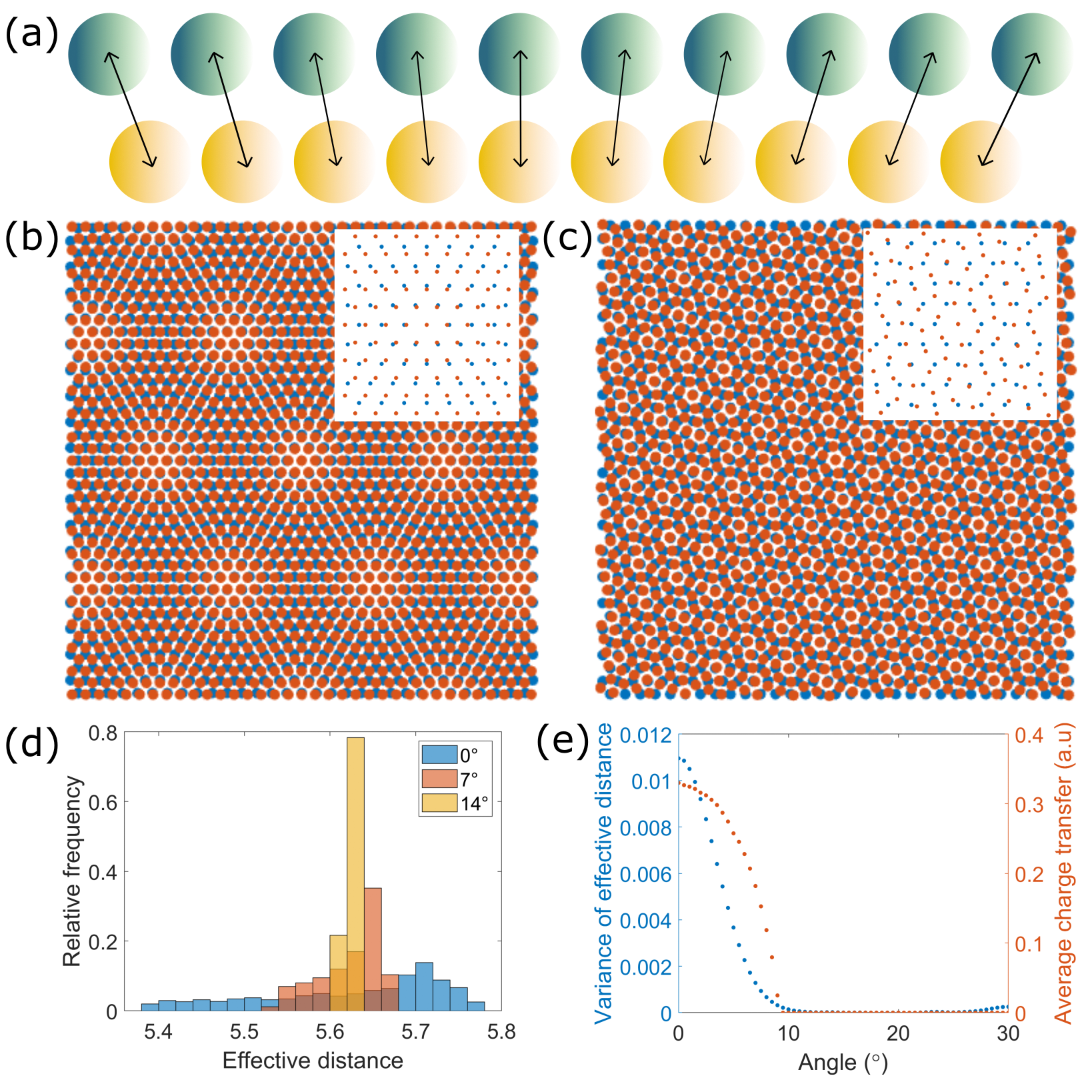
Considering a flat MoS2 ML on Au(111), we construct a simple model to understand the twist angle dependence of the electronic structure. We assume that the hybridization is primarily determined by the nearest neighbor distances (NND) between S and Au atoms shown as green and yellow spheres in Figure 5(a), respectively. The schematic top views in Figure 5(b) and (c) illustrate the changing registry of these two atomic layers as a function of twist angle and the resulting moiré patterns with spatially modulated NND. The distribution of the distances between the nearest S and Au atoms is independent of the twist angle (see inset in Figure 5(b) and (c)). In particular, the number of S atoms sitting on top of a Au atom per unit area is the same for all twist angles. Based on the registry between S and Au atoms alone, one would thus not expect any twist angle dependence of the amplitude of the modulated hybridization, in contradiction with the experimental observation. However, looking only at the NND to quantify the hybridization is not physically plausible: it neglects screening which prevents abrupt changes in the charge distribution over very short distances [37]. To take this into account we, introduce an effective distance obtained by convoluting the spatial distribution of NNDs with a Gaussian. By construction, is spatially modulated at the moiré period and provides a measure of the strength of the local hybridization: it is stronger where is smaller.
While the distribution of the distances between nearest S and Au atoms does not depend on twist angle, their spatial distribution does, with significantly larger site-to-site variations at larger twist angles as seen in Figure 5(b) and (c). These abrupt changes are attenuated by screening, leading to an increasingly narrow distribution of , as shown by the histograms in Figure 5(d) for 0°, 7°, and 14° twist angles, which correspond to an increasingly homogeneous . To assess the amplitude of the modulated hybridization, we plot the variance of (which reflects the width of its distribution) as a function of twist angle in Figure 5(e). This clearly shows that the spatial variation of the hybridization vanishes with increasing twist angle, which explains the correlation between large twist angles and more homogeneous electronic properties observed in Figures 3 and 4.
The average of the VBM and the average of the CBm both shift down in energy, with a larger shift for smaller twist angles (Figure 4(c)). This indicates a stronger electron doping with a larger overall charge transfer when the twist angle is small. The amount of charge transferred at a given site is a function of the local : . The average charge transfer (i.e. charge transfer per Au-S pair for pairs) is
| (1) |
To gain insight into the twist angle dependence of within our simple model, we note that although the distribution of depends on twist angle, its spatial average is constant (SI Section \Romannum7). It means that is not a linear function. We consider two simple non-linear models which reproduce a stronger charge transfer for the Au-S pairs where is shorter. Both models yield the same qualitative result.
The first model is motivated by the finding of Silva et al. [34] in MBE-grown films (0.5° twist angle) that all the bottom S atoms of the MoS2 ML fall into either of two categories: strongly bound or weakly bound to the underlying Au atom. Thus we consider two kinds of S atoms, one that contributes significantly (the strongly bound) and one that does not contribute to the charge transfer (the weakly bound). Assuming a given fraction (e.g. ) of significantly contributing S atoms in the 0° twist angle heterostructure, we can estimate a general cut-off below (above) which all S-Au pairs fall in the strongly (weakly) bound category with significant (negligible) charge transfer at a given twist angle. In this case
| (2) |
In Figure 5(e) (right orange axis) we show as a function of twist angle calculated using Equation 2. We find that monotonically decreases as a function of the twist angle, which reproduces the observed overall decreasing charge transfer with increasing twist angle. We obtain the same result with another non-linear function , as shown in SI Section \Romannum7.
III Conclusions
We present a systematic study of the twist-angle dependent electronic properties of exfoliated MoS2 monolayers on Au(111) using high-resolution scanning tunneling microscopy and spectroscopy. We find that the conduction and valence bands are modulated at the moiré pattern period. The modulations are most prominent in the valence band and largest for the smaller twist angles. They vanish with increasing twist angles. We propose a simple model to understand this twist angle dependence based on a changing hybridization between S and Au orbitals, which does not only depend on the relative positions of the nearest S and Au atoms, but also on their neighboring configurations. These findings provide detailed insight into designing monolayer-on-metal heterostructures with variable electronic properties and doping by adjusting the twist angle. They also provide a platform to explore correlated and ordered electronic phases in combination with periodic charge transfer (or doping) patterns.
IV Methods
We use gold-assisted exfoliation [21, 23, 27] onto template-stripped gold substrates [24, 38] to mechanically isolate MoS2 monolayers (MLs). The gold substrates are prepared in-house. First, we evaporate gold onto a clean ultra-flat silicon (Si) wafer. Second, we epoxy another flat Si piece onto the crystalline gold film. We then cleave this sandwich at the evaporated Au-Si interface to get an ultra-flat gold surface that reflects the flatness of the original Si substrate. Bulk 2H-MoS2 single crystals were sourced from HQ graphene. These crystals are exfoliated to the monolayer limit onto the freshly exposed Au surface in a nitrogen-filled glove box, using scotch-tape exfoliation. The strong affinity between sulfur and the very clean and flat template-stripped Au substrate allows us to obtain millimeter-sized MoS2 MLs. We identify ML MoS2 flakes based on their optical contrast on gold and using Raman spectroscopy. A detailed characterization of the gold substrate and of the MoS2-on-Au heterostructures is presented in the Supplementary Information Sections \Romannum1 and \Romannum3. Landing the STM tip on a desired region on the flake is performed using optical microscopy images. Throughout the process, we carefully protect the samples from exposure to the ambient atmosphere to avoid contamination and device degradation. For Raman and optical measurements, the samples were placed in a customized air-tight container with optical access that can be sealed in a glove box. For transferring the samples from the glove box to the STM, we used a home-built vacuum suitcase which can be directly attached to the load-lock of the ultra-high vacuum STM chamber. Prior to the STM measurements, the samples were annealed in situ at 150° C for about 100 hours to obtain an optimal surface.
All the scanning tunneling microscopy and spectroscopy experiments were done using a Specs JT Tyto STM at 77.7 K or 5 K, at a base pressure better than 1 mBar. We used electrochemically etched W or Ir tips, all carefully conditioned and characterized in situ on Au(111) single crystal. STM topographic images were recorded in constant current mode. conductance curves were acquired using a lock-in with a sample bias modulation amplitude of 15 mV at 527 Hz.
For the qualitative modeling of the twist angle-dependent hybridization, we considered a large number of atoms (of the order of ) in each layer to minimize finite size effects.
ACKNOWLEDGEMENTS
We thank A.F. Morpurgo for providing access to glove box, evaporator, and AFM facilities. We thank A. Scarfato and I. Maggio-Aprile for stimulating scientific discussions, and A. Guipet and G. Manfrini for technical support in the STM laboratory. We also thank A. Ørsted and J.C. Crost for helping with the first attempts to prepare the Au substrates and J. Teyssier for his assistance with the Raman measurements. This work was supported by the Swiss National Science Foundation (Division II Grant No. 182652).
References
- [1] J. Kim, C. Jin, B. Chen, H. Cai, T. Zhao, P. Lee, S. Kahn, K. Watanabe, T. Taniguchi, S. Tongay, M. F. Crommie, and F. Wang, “Observation of ultralong valley lifetime in WSe2/MoS2 heterostructures,” Science Advances, vol. 3, no. 7, p. e1700518.
- [2] T. Naimer, K. Zollner, M. Gmitra, and J. Fabian, “Twist-angle dependent proximity induced spin-orbit coupling in graphene/transition metal dichalcogenide heterostructures,” Physical Review B, vol. 104, no. 19, p. 195156, 2021.
- [3] D. Pei, B. Wang, Z. Zhou, Z. He, L. An, S. He, C. Chen, Y. Li, L. Wei, A. Liang, J. Avila, P. Dudin, V. Kandyba, A. Giampietri, M. Cattelan, A. Barinov, Z. Liu, J. Liu, H. Weng, N. Wang, J. Xue, and Y. Chen, “Observation of -valley moiré bands and emergent hexagonal lattice in twisted transition metal dichalcogenides,” Physical Review X, vol. 12, no. 2, p. 021065, 2022.
- [4] Y. Cao, V. Fatemi, S. Fang, K. Watanabe, T. Taniguchi, E. Kaxiras, and P. Jarillo-Herrero, “Unconventional superconductivity in magic-angle graphene superlattices,” Nature, vol. 556, no. 7699, pp. 43–50, 2018.
- [5] J. D. Sanchez-Yamagishi, T. Taychatanapat, K. Watanabe, T. Taniguchi, A. Yacoby, and P. Jarillo-Herrero, “Quantum hall effect, screening, and layer-polarized insulating states in twisted bilayer graphene,” Physical Review Letters, vol. 108, no. 7, p. 076601, 2012.
- [6] A. K. Geim and I. V. Grigorieva, “Van der Waals heterostructures,” Nature, vol. 499, no. 7459, pp. 419–425, 2013.
- [7] Y. Chen, L. Wu, H. Xu, C. Cong, S. Li, S. Feng, H. Zhang, C. Zou, J. Shang, S. A. Yang, K. P. Loh, W. Huang, and T. Yu, “Visualizing the anomalous charge density wave states in graphene/NbSe2 heterostructures,” Advanced Materials, vol. 32, no. 45, p. 2003746, 2020.
- [8] Y.-C. Lin, C.-Y. S. Chang, R. K. Ghosh, J. Li, H. Zhu, R. Addou, B. Diaconescu, T. Ohta, X. Peng, N. Lu, M. J. Kim, J. T. Robinson, R. M. Wallace, T. S. Mayer, S. Datta, L.-J. Li, and J. A. Robinson, “Atomically thin heterostructures based on single-layer tungsten diselenide and graphene,” Nano Letters, vol. 14, no. 12, pp. 6936–6941, 2014.
- [9] D. Rhodes, S. H. Chae, R. Ribeiro-Palau, and J. Hone, “Disorder in van der waals heterostructures of 2D materials,” Nature Materials, vol. 18, no. 6, pp. 541–549, 2019.
- [10] Q. Wu, M. Bagheri Tagani, L. Zhang, J. Wang, Y. Xia, L. Zhang, S.-Y. Xie, Y. Tian, L.-J. Yin, W. Zhang, A. N. Rudenko, A. T. S. Wee, P. K. J. Wong, and Z. Qin, “Electronic tuning in WSe2/Au via van der Waals interface twisting and intercalation,” ACS Nano, vol. 16, no. 4, pp. 6541–6551, 2022.
- [11] S. S. Grønborg, S. Ulstrup, M. Bianchi, M. Dendzik, C. E. Sanders, J. V. Lauritsen, P. Hofmann, and J. A. Miwa, “Synthesis of epitaxial single-layer MoS2 on Au(111),” Langmuir, vol. 31, no. 35, pp. 9700–9706, 2015.
- [12] S. Yasuda, R. Takahashi, R. Osaka, R. Kumagai, Y. Miyata, S. Okada, Y. Hayamizu, and K. Murakoshi, “Out-of-plane strain induced in a moiré superstructure of monolayer MoS2 and MoSe2 on Au(111),” Small, vol. 13, no. 31, p. 1700748, 2017.
- [13] X. Zhou, J. Shi, Y. Qi, M. Liu, D. Ma, Y. Zhang, Q. Ji, Z. Zhang, C. Li, Z. Liu, and Y. Zhang, “Periodic modulation of the doping level in striped MoS2 superstructures,” ACS Nano, vol. 10, no. 3, pp. 3461–3468, 2016.
- [14] P. Yang, S. Zhang, S. Pan, B. Tang, Y. Liang, X. Zhao, Z. Zhang, J. Shi, Y. Huan, Y. Shi, S. J. Pennycook, Z. Ren, G. Zhang, Q. Chen, X. Zou, Z. Liu, and Y. Zhang, “Epitaxial growth of centimeter-scale single-crystal MoS2 monolayer on Au(111),” ACS Nano, vol. 14, no. 4, pp. 5036–5045, 2020.
- [15] J. Li, S. Wang, Q. Jiang, H. Qian, S. Hu, H. Kang, C. Chen, X. Zhan, A. Yu, S. Zhao, Y. Zhang, Z. Chen, Y. Sui, S. Qiao, G. Yu, S. Peng, Z. Jin, and X. Liu, “Single-crystal MoS2 monolayer wafer grown on Au(111) film substrates,” Small, vol. 17, no. 30, p. 2100743, 2021.
- [16] F. Wu, Z. Liu, N. Hawthorne, M. Chandross, Q. Moore, N. Argibay, J. F. Curry, and J. D. Batteas, “Formation of coherent 1H–1T heterostructures in single-layer MoS2 on Au(111),” ACS Nano, vol. 14, no. 12, pp. 16939–16950, 2020.
- [17] B. T. Blue, G. G. Jernigan, D. Le, J. J. Fonseca, S. D. Lough, J. E. Thompson, D. D. Smalley, T. S. Rahman, J. T. Robinson, and M. Ishigami, “Metallicity of 2H-MoS2 induced by Au hybridization,” 2D Materials, vol. 7, no. 2, p. 025021, 2020.
- [18] J. Pető, G. Dobrik, G. Kukucska, P. Vancsó, A. A. Koós, J. Koltai, P. Nemes-Incze, C. Hwang, and L. Tapasztó, “Moderate strain induced indirect bandgap and conduction electrons in MoS2 single layers,” npj 2D Materials and Applications, vol. 3, no. 1, p. 39, 2019.
- [19] P. Vancsó, G. Z. Magda, J. Pető, J.-Y. Noh, Y.-S. Kim, C. Hwang, L. P. Biró, and L. Tapasztó, “The intrinsic defect structure of exfoliated MoS2 single layers revealed by scanning tunneling microscopy,” Scientific Reports, vol. 6, no. 1, p. 29726, 2016.
- [20] J. Pető, T. Ollár, P. Vancsó, Z. I. Popov, G. Z. Magda, G. Dobrik, C. Hwang, P. B. Sorokin, and L. Tapasztó, “Spontaneous doping of the basal plane of MoS2 single layers through oxygen substitution under ambient conditions,” Nature Chemistry, vol. 10, no. 12, pp. 1246–1251, 2018.
- [21] G. Z. Magda, J. Pető, G. Dobrik, C. Hwang, L. P. Biró, and L. Tapasztó, “Exfoliation of large-area transition metal chalcogenide single layers,” Scientific Reports, vol. 5, no. 1, p. 14714, 2015.
- [22] S. M. Hus, R. Ge, P.-A. Chen, L. Liang, G. E. Donnelly, W. Ko, F. Huang, M.-H. Chiang, A.-P. Li, and D. Akinwande, “Observation of single-defect memristor in an MoS2 atomic sheet,” Nature Nanotechnology, vol. 16, no. 1, pp. 58–62, 2021.
- [23] Y. Huang, Y.-H. Pan, R. Yang, L.-H. Bao, L. Meng, H.-L. Luo, Y.-Q. Cai, G.-D. Liu, W.-J. Zhao, Z. Zhou, L.-M. Wu, Z.-L. Zhu, M. Huang, L.-W. Liu, L. Liu, P. Cheng, K.-H. Wu, S.-B. Tian, C.-Z. Gu, Y.-G. Shi, Y.-F. Guo, Z. G. Cheng, J.-P. Hu, L. Zhao, G.-H. Yang, E. Sutter, P. Sutter, Y.-L. Wang, W. Ji, X.-J. Zhou, and H.-J. Gao, “Universal mechanical exfoliation of large-area 2D crystals,” Nature Communications, vol. 11, no. 1, p. 2453, 2020.
- [24] M. Hegner, P. Wagner, and G. Semenza, “Ultralarge atomically flat template-stripped Au surfaces for scanning probe microscopy,” Surface Science, vol. 291, no. 1, pp. 39–46, 1993.
- [25] M. Velický, A. Rodriguez, M. Bouša, A. V. Krayev, M. Vondráček, J. Honolka, M. Ahmadi, G. E. Donnelly, F. Huang, H. D. Abruña, K. S. Novoselov, and O. Frank, “Strain and charge doping fingerprints of the strong interaction between monolayer MoS2 and gold,” The Journal of Physical Chemistry Letters, vol. 11, no. 15, pp. 6112–6118, 2020.
- [26] E. Pollmann, S. Sleziona, T. Foller, U. Hagemann, C. Gorynski, O. Petri, L. Madauß, L. Breuer, and M. Schleberger, “Large-area, two-dimensional MoS2 exfoliated on gold: Direct experimental access to the metal–semiconductor interface,” ACS Omega, vol. 6, no. 24, pp. 15929–15939, 2021.
- [27] M. Velický, G. E. Donnelly, W. R. Hendren, S. McFarland, D. Scullion, W. J. I. DeBenedetti, G. C. Correa, Y. Han, A. J. Wain, M. A. Hines, D. A. Muller, K. S. Novoselov, H. D. Abruña, R. M. Bowman, E. J. G. Santos, and F. Huang, “Mechanism of gold-assisted exfoliation of centimeter-sized transition-metal dichalcogenide monolayers,” ACS Nano, vol. 12, no. 10, pp. 10463–10472, 2018.
- [28] A. Kerelsky, A. Nipane, D. Edelberg, D. Wang, X. Zhou, A. Motmaendadgar, H. Gao, S. Xie, K. Kang, J. Park, J. Teherani, and A. Pasupathy, “Absence of a band gap at the interface of a metal and highly doped monolayer MoS2,” Nano Letters, vol. 17, no. 10, pp. 5962–5968, 2017.
- [29] X. Zhou, K. Kang, S. Xie, A. Dadgar, N. R. Monahan, X. Y. Zhu, J. Park, and A. N. Pasupathy, “Atomic-scale spectroscopy of gated monolayer MoS2,” Nano Letters, vol. 16, no. 5, pp. 3148–3154, 2016.
- [30] N. Krane, C. Lotze, J. M. Läger, G. Reecht, and K. J. Franke, “Electronic structure and luminescence of quasi-freestanding MoS2 nanopatches on Au(111),” Nano Letters, vol. 16, no. 8, pp. 5163–5168, 2016.
- [31] E. Ponomarev, A. Pásztor, A. Waelchli, A. Scarfato, N. Ubrig, C. Renner, and A. F. Morpurgo, “Hole transport in exfoliated monolayer MoS2,” ACS Nano, vol. 12, no. 3, pp. 2669–2676, 2018.
- [32] A. Bruix, J. A. Miwa, N. Hauptmann, D. Wegner, S. Ulstrup, S. S. Grønborg, C. E. Sanders, M. Dendzik, A. Grubišić Čabo, M. Bianchi, J. V. Lauritsen, A. A. Khajetoorians, B. Hammer, and P. Hofmann, “Single-layer MoS2 on Au(111): Band gap renormalization and substrate interaction,” Physical Review B, vol. 93, no. 16, p. 165422, 2016.
- [33] N. Krane, C. Lotze, and K. J. Franke, “Moiré structure of MoS2 on Au(111): Local structural and electronic properties,” Surface Science, vol. 678, pp. 136–142, 2018.
- [34] C. C. Silva, D. Dombrowski, N. Atodiresei, W. Jolie, F. Farwick zum Hagen, J. Cai, P. T. P. Ryan, P. K. Thakur, V. Caciuc, S. Blügel, D. A. Duncan, T. Michely, T.-L. Lee, and C. Busse, “Spatial variation of geometry, binding, and electronic properties in the moiré superstructure of MoS2 on Au(111),” 2D Materials, vol. 9, no. 2, p. 025003, 2022.
- [35] K. Reidy, G. Varnavides, J. D. Thomsen, A. Kumar, T. Pham, A. M. Blackburn, P. Anikeeva, P. Narang, J. M. LeBeau, and F. M. Ross, “Direct imaging and electronic structure modulation of moiré superlattices at the 2D/3D interface,” Nature Communications, vol. 12, no. 1, p. 1290, 2021.
- [36] C. J. Chen, Introduction to Scanning Tunneling Microscopy Third Edition, vol. 69. Oxford University Press, USA, 2021.
- [37] Q. Zhang, J. Yu, P. Ebert, C. Zhang, C.-R. Pan, M.-Y. Chou, C.-K. Shih, C. Zeng, and S. Yuan, “Tuning band gap and work function modulations in monolayer hBN/Cu(111) heterostructures with moiré patterns,” ACS Nano, vol. 12, no. 9, pp. 9355–9362, 2018.
- [38] N. Vogel, J. Zieleniecki, and I. Köper, “As flat as it gets: ultrasmooth surfaces from template-stripping procedures,” Nanoscale, vol. 4, no. 13, pp. 3820–3832, 2012.